Download as PDF, PPTX


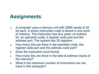
![Exercise 2
The following register transfers are to be executed in our System.
For each transfer, specify (1). the binary value to be applied to bus
select inputs S0,S1, S2. (2) the register whose LD control must be
active (3) a memory READ or Write (if needed) (4) the operation in
the adder & logic circuit.
a. AR PC
b. IR M[AR]
c. M[AR]TR
d. ACDR, DRAC (done simultaneously)](https://image.slidesharecdn.com/rygm7bkoqaiyhv7ypnjk-signature-0a4922234e76dd63e069a6bd18dc04eb91d65155d5eb6817e3dd5da56ee52bda-poli-170322104337/85/Lect11-organization-22-320.jpg)
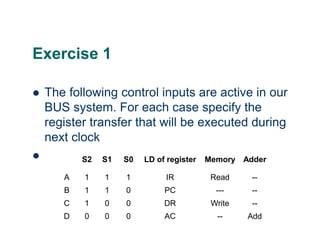
![Exercise 3
Explain why each of the following
microoperations cannot be executed during a
single clock in the system.
a. IRM[PC]
b. AC AC+TR
c. DR DR + AC (AC does not change)](https://image.slidesharecdn.com/rygm7bkoqaiyhv7ypnjk-signature-0a4922234e76dd63e069a6bd18dc04eb91d65155d5eb6817e3dd5da56ee52bda-poli-170322104337/85/Lect11-organization-23-320.jpg)

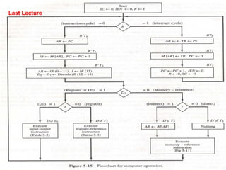
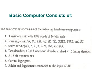
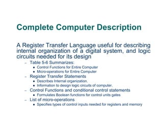
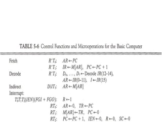
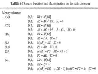
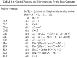
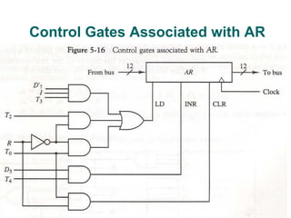
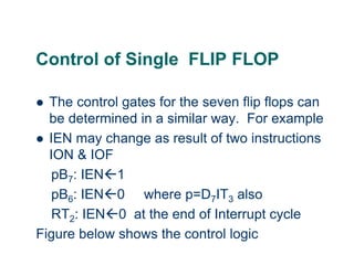
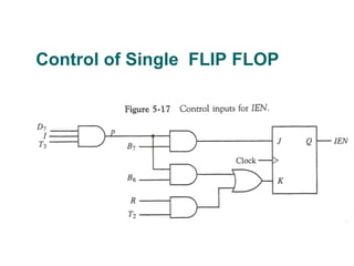
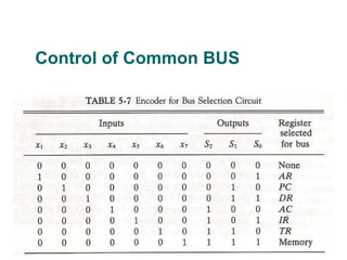
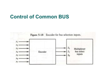
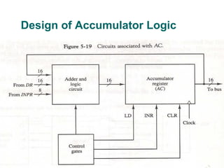
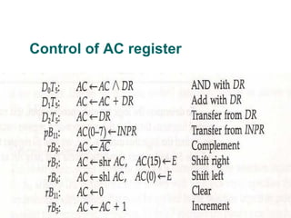
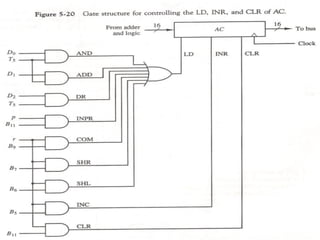
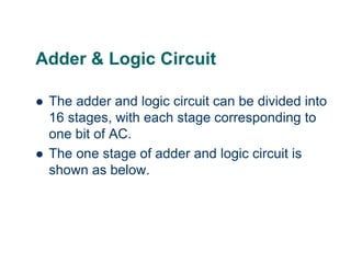
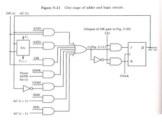
This document describes the internal organization and logic circuits of a computer system using a register transfer language. It includes: 1) A table summarizing the control functions and micro-operations for the entire computer. This describes the internal organization and allows designing the computer's logic circuits. 2) Examples of register transfer statements and control functions/conditional statements that formulate the control unit's Boolean functions. 3) A list of micro-operations specifying the types of control inputs needed for registers and memory. 4) Diagrams showing the control logic for flip-flops and buses, the accumulator logic, and an adder/logic circuit stage. 5) Examples of exercises analyzing register transfers and microoperations in the system