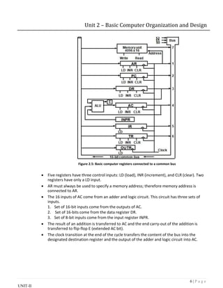
The document describes the basic components and organization of a computer system, including instruction codes, operation codes, registers, memory, and control unit.
It discusses the different parts of an instruction code, including the operation code and address. It describes the registers in the computer, including the accumulator, instruction register, and program counter. The computer uses a common bus to transfer data between registers and memory.
The control unit increments a sequence counter to generate timing signals that control data transfer and instruction execution. It can reset the counter based on the instruction operation code to change the sequence.


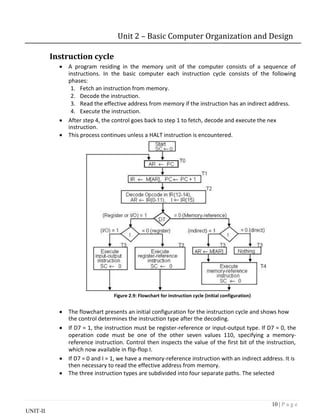
![11 | P a g e
UNIT-II
Unit 2 – Basic Computer Organization and Design
operation is activated with the clock transition associated with timing signal T3.This can
be symbolized as follows:
D’7 I T3: AR
M [AR]
D’7 I’ T3: Nothing
D7 I’ T3: Execute a register-reference instruction
D7 I T3: Execute an input-output instruction
When a memory-reference instruction with I = 0 is encountered, it is not necessary to do
anything since the effective address is already in AR.
However, the sequence counter SC must be incremented when D’7 I T3 = 1, so that the
execution of the memory-reference instruction can be continued with timing variable T4.
A register-reference or input-output instruction can be executed with the click
associated with timing signal T3. After the instruction is executed, SC is cleared to 0 and
control returns to the fetch phase with T0 =1. SC is either incremented or cleared to 0
with every positive clock transition.
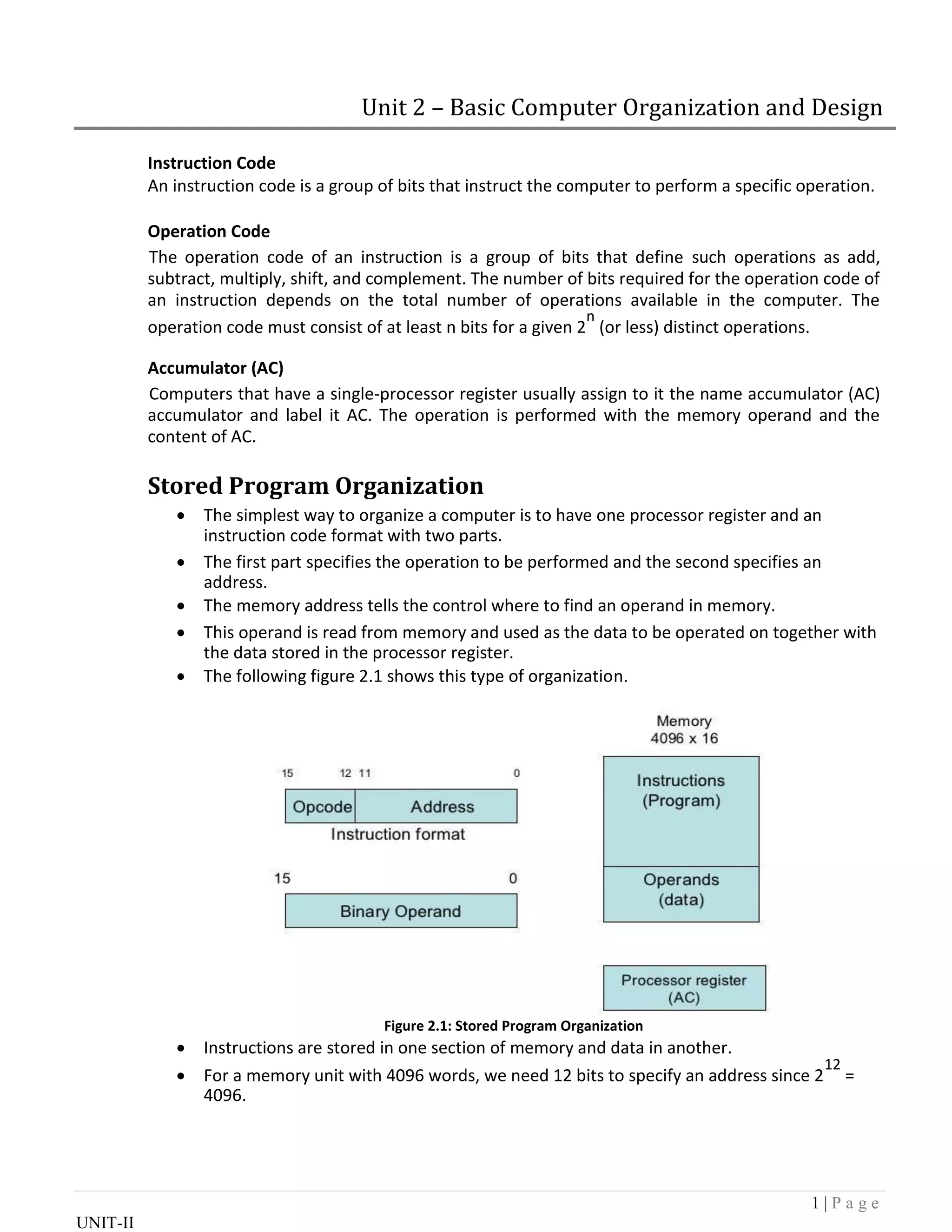
Register reference instruction.
When the register-reference instruction is decoded, D7 bit is set to 1.
Each control function needs the Boolean relation D7 I' T3
15 12 11 0
0 1 1 1 Register Operation
There are 12 register-reference instructions listed below:
r: SC0 Clear SC
CLA rB11: AC 0 Clear AC
CLE rB10: E 0 Clear E
CMA rB9: AC AC’ Complement AC
CME rB8: E E’ Complement E
CIR rB7: AC shr AC, AC(15) E, E AC(0) Circular Right
CIL rB6: AC shl AC, AC(0) E, E AC(15) Circular Left
INC rB5: AC AC + 1 Increment AC
SPA rB4: if (AC(15) = 0) then (PC PC+1) Skip if positive
SNA rB3: if (AC(15) = 1) then (PC PC+1 Skip if negative
SZA rB2: if (AC = 0) then (PC PC+1) Skip if AC is zero
SZE rB1: if (E = 0) then (PC PC+1) Skip if E is zero
HLT rB0: S 0 (S is a start-stop flip-flop) Halt computer
These 12 bits are available in IR (0-11). They were also transferred to AR during time T2.
These instructions are executed at timing cycle T3.
The first seven register-reference instructions perform clear, complement, circular shift,
and increment microoperations on the AC or E registers.
The next four instructions cause a skip of the next instruction in sequence when](https://image.slidesharecdn.com/computerorganization-230216171710-e6b0abcb/85/computer-organization-pdf-11-320.jpg)
![12 | P a g e
UNIT-II
Unit 2 – Basic Computer Organization and Design
condition is satisfied. The skipping of the instruction is achieved by incrementing PC.
The condition control statements must be recognized as part of the control conditions.
The AC is positive when the sign bit in AC(15) = 0; it is negative when AC(15) = 1. The
content of AC is zero (AC = 0) if all the flip-flops of the register are zero.
The HLT instruction clears a start-stop flip-flop S and stops the sequence counter from
counting. To restore the operation of the computer, the start-stop flip-flop must be set
manually.
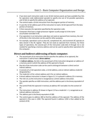
Memory reference instructions
When the memory-reference instruction is decoded, D7 bit is set to 0.
15 14 12 11 0
I 000~110 Address
The following table lists seven memory-reference instructions.
Symbol Operation Symbolic Description
Decoder
AND D0 AC AC M[AR]
ADD D1 AC AC + M[AR], E Cout
LDA D2 AC M[AR]
STA D3 M[AR] AC
BUN D4 PC AR
BSA D5 M[AR] PC, PC AR + 1
ISZ D6 M[AR] M[AR] + 1, if M[AR] + 1 = 0 then PC PC+1
The effective address of the instruction is in the address register AR and was placed
there during timing signal T2 when I = 0, or during timing signal T3 when I = 1.
The execution of the memory-reference instructions starts with timing signal T4.
AND to AC
This is an instruction that performs the AND logic operation on pairs of bits in AC and the
memory word specified by the effective address. The result of the operation is
transferred to AC.
D0T4: DRM[AR]
D0T5: AC AC DR, SC 0
ADD to AC
This instruction adds the content of the memory word specified by the effective address
to the value of AC. The sum is transferred into AC and the output carry Cout is transferred
to the E (extended accumulator) flip-flop.
D1T4: DR M[AR]
D1T5: AC AC + DR, E Cout, SC 0](https://image.slidesharecdn.com/computerorganization-230216171710-e6b0abcb/85/computer-organization-pdf-12-320.jpg)
![13 | P a g e
UNIT-II
Unit 2 – Basic Computer Organization and Design
LDA: Load to AC
This instruction transfers the memory word specified by the effective address to AC.
D2T4: DR M[AR]
D2T5: AC DR, SC 0
STA: Store AC
This instruction stores the content of AC into the memory word specified by the effective
address.
D3T4: M[AR] AC, SC 0
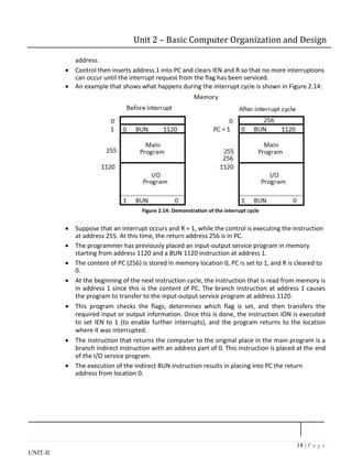
BUN: Branch Unconditionally
This instruction transfers the program to instruction specified by the effective address.
The BUN instruction allows the programmer to specify an instruction out of sequence
and the program branches (or jumps) unconditionally.
D4T4: PC AR, SC 0
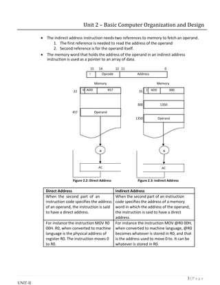
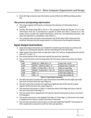
BSA: Branch and Save Return Address
This instruction is useful for branching to a portion of the program called a subroutine or
procedure. When executed, the BSA instruction stores the address of the next
instruction in sequence (which is available in PC) into a memory location specified by the
effective address.
M[AR] PC, PC AR + 1
M[135] 21, PC 135 + 1 = 136
Figure2.10: Example of BSA instruction execution
It is not possible to perform the operation of the BSA instruction in one clock cycle when
we use the bus system of the basic computer. To use the memory and the bus properly,
the BSA instruction must be executed with a sequence of two microoperations:
D5T4: M[AR] PC, AR AR + 1
D5T5: PC AR, SC 0
ISZ: Increment and Skip if Zero
These instruction increments the word specified by the effective address, and if the
incremented value is equal to 0, PC is incremented by 1. Since it is not possible to](https://image.slidesharecdn.com/computerorganization-230216171710-e6b0abcb/85/computer-organization-pdf-13-320.jpg)
![14 | P a g e
UNIT-II
Unit 2 – Basic Computer Organization and Design
increment a word inside the memory, it is necessary to read the word into DR, increment
DR, and store the word back into memory.
D6T4: DR M[AR]
D6T5: DR DR + 1
D6T4: M[AR] DR, if (DR = 0) then (PC PC + 1), SC 0
Control Flowchart
Figure 2.11: Flowchart for memory-reference instructions](https://image.slidesharecdn.com/computerorganization-230216171710-e6b0abcb/85/computer-organization-pdf-14-320.jpg)
![19 | P a g e
UNIT-II
Unit 2 – Basic Computer Organization and Design
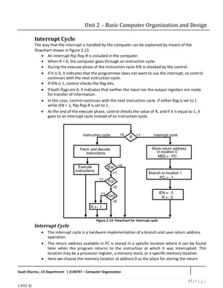
Register transfer statements for the interrupt cycle
The flip-flop is set to 1 if IEN = 1 and either FGI or FGO are equal to 1. This can happen
with any clock transition except when timing signals T0, T1 or T2 are active.
The condition for setting flip-flop R= 1 can be expressed with the following register
transfer statement:
T0T1T2 (IEN) (FGI + FGO): R 1
The symbol + between FGI and FGO in the control function designates a logic OR
operation. This is AND with IEN and T0T1 T2 .
The fetch and decode phases of the instruction cycle must be modified and Replace T0,
T1, T2 with R'T0, R'T1, R'T2
Therefore the interrupt cycle statements are :
RT0: AR 0, TR PC
RT1: M[AR] TR, PC 0
RT2: PC PC + 1, IEN 0, R 0, SC 0
During the first timing signal AR is cleared to 0, and the content of PC is transferred to
the temporary register TR.
With the second timing signal, the return address is stored in memory at location 0 and
PC is cleared to 0.
The third timing signal increments PC to 1, clears IEN and R, and control goes back to T0
by clearing SC to 0.
The beginning of the next instruction cycle has the condition RT0 and the content of PC is
equal to 1. The control then goes through an instruction cycle that fetches and executes
the BUN instruction in location 1.
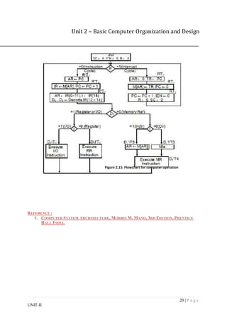
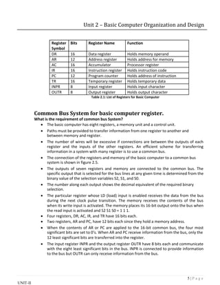
Flow chart for computer operation.
The final flowchart of the instruction cycle, including the interrupt cycle for the basic
computer, is shown in Figure 2.15.
The interrupt flip-flop R may be set at any time during the indirect or execute phases.
The control returns to timing signal T0 after SC is cleared to 0.
If R = 1, the computer goes through an interrupt cycle. If R = 0, the computer goes
through an instruction cycle.
If the instruction is one of the memory-reference instructions, the computer first checks
if there is an indirect address and then continues to execute the decoded instruction
according to the flowchart.
If the instruction is one of the register-reference instructions, it is executed with one of
the microoperations register reference.
If it is an input-output instruction, it is executed with one of the microoperation’s input-
output reference.](https://image.slidesharecdn.com/computerorganization-230216171710-e6b0abcb/85/computer-organization-pdf-19-320.jpg)