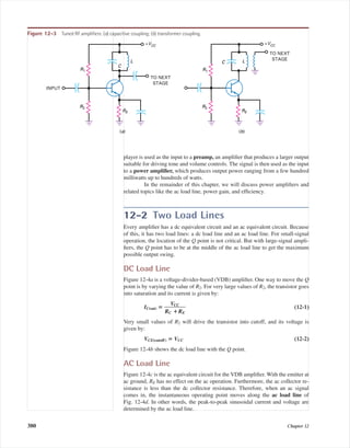
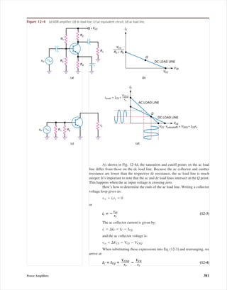
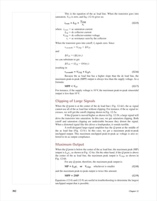
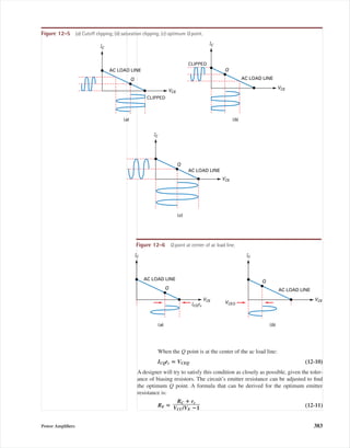
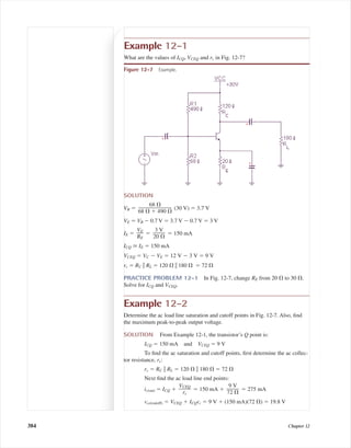
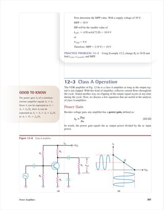
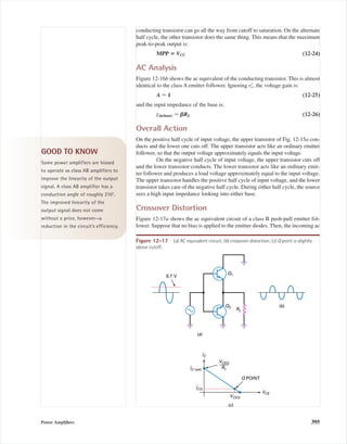
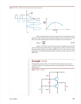
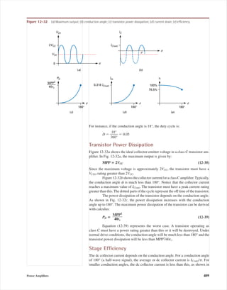
The document discusses power amplifiers and related concepts. It explains that power amplifiers have both a DC load line and an AC load line. The DC load line determines the quiescent operating point (Q point) while the AC load line determines the maximum output swing. For optimal performance without clipping, the Q point should be located at the center of the AC load line. The maximum unclipped peak-to-peak output is determined by either the product of collector current and AC resistance, or collector-emitter voltage - whichever is smaller. Proper biasing of the amplifier, including adjustment of the emitter resistance, can be used to position the Q point optimally on the AC load line.
International Refereed Journal of Engineering and Science (IRJES)irjes
International Refereed Journal of Engineering and Science (IRJES) is a leading international journal for publication of new ideas, the state of the art research results and fundamental advances in all aspects of Engineering and Science. IRJES is a open access, peer reviewed international journal with a primary objective to provide the academic community and industry for the submission of half of original research and applications.
This document discusses a dual mode series resonant DC-DC converter that can operate efficiently over a wide range of load variations. It presents a converter design that uses a full-bridge topology with series resonant components. The converter can operate in two modes - a switching frequency modulation mode for normal to high loads, and a phase shifted pulse width modulation mode for light loads. The dual mode operation allows for high conversion efficiency across the wide load range. Key aspects of the resonant converter design and operating principles are explained.
This document proposes a new passive power factor correction (PFC) circuit for flyback converters using an improved valley fill method. The circuit adds an extra winding magnetically coupled to the flyback transformer and electrically coupled to valley fill capacitors. This allows the capacitors to be charged through a high frequency inductor, reducing current spikes and total harmonic distortion. The proposed circuit provides PFC without an active switch, using low voltage capacitors at half the peak line voltage. Experimental results show the circuit achieves higher power factor and lower harmonic distortion than conventional valley fill methods.
2 twofold mode series echoing dc dc converter for ample loadchelliah paramasivan
The document describes a dual-mode full-bridge series resonant DC-DC converter that can operate at either a variable switching frequency or a fixed switching frequency with phase-shifted pulse width modulation to regulate the output voltage over a wide range of loads. The converter uses a series resonant tank consisting of an inductor and capacitor to achieve soft switching and zero voltage switching of the transistors. It can operate in a frequency modulation mode at high loads by varying the switching frequency, or in a phase modulation mode at light loads using a fixed high switching frequency and varying the duty cycle through phase-shifted pulse width modulation. This dual-mode operation provides high conversion efficiency across a wide range of loads.
This document discusses transmission lines and their parameters. It begins by introducing transmission lines as guided structures that direct the propagation of energy from a source to a load. It then discusses the key parameters used to describe transmission lines - resistance, inductance, conductance and capacitance per unit length. It provides examples of how electromagnetic waves propagate through transmission lines and derives the transmission line equations. It also covers input impedance, standing wave ratio, power, and gives examples of calculating transmission line properties. The document concludes by discussing microstrip transmission lines.
Power Amplifiers: Classification of amplifiers, Class A power Amplifiers and their analysis, Harmonic Distortions,
Class B Push-pull amplifiers and their analysis, Complementary symmetry push pull amplifier, Class AB power
amplifier, Class-C power amplifier, Thermal stability and Heat sinks, Distortion in amplifiers.
Electronics and Communication Engineering is the Branch of Engineering. Electronics and Communication Engineering field requires an understanding of core areas including Engineering Graphics, Computer Programming,Electronics Devices and Circuits-I, Network Analysis, Signals and Systems, Communication Systems, Electromagnetics Engineering, Digital Signal Processing, Embedded Systems, Microprocessor and Computer Architecture. Ekeeda offers Online Mechanical Engineering Courses for all the Subjects as per the Syllabus. Visit : https://ekeeda.com/streamdetails/stream/Electronics-and-Communication-Engineering
This document provides an introduction to bipolar junction transistors (BJTs). It discusses that BJTs are made of two back-to-back p-n junctions and are three-layer devices consisting of either two n-type and one p-type layers or two p-type and one n-type layers. The document describes the formation and operation of p-n-p and n-p-n transistors. It discusses forward biasing of the emitter-base junction, the majority and minority carrier currents, and the different current components in BJTs. The document also covers the common-base, common-emitter, and common-collector configurations and their input and output characteristics.
This document discusses transmission line basics and concepts. It covers transmission line equivalent circuits, relevant equations for propagation and characteristic impedance, and examples of transmission line structures. It also discusses reflection coefficients and diagrams, and provides formulas for calculating per-unit length capacitance, inductance, impedance, and propagation delay of transmission lines. Special cases for reflection coefficients when a transmission line is terminated in its characteristic impedance, presents an open circuit, or is short circuited are also summarized.
This document provides an overview of transmission line basics and concepts. It discusses key transmission line parameters like characteristic impedance, propagation delay, per-unit-length capacitance and inductance. It covers transmission line equivalent circuit models and relevant equations. It also discusses transmission line structures, parallel plate approximations, reflection coefficients, and discontinuities. The goal is to understand transmission line behavior and analysis techniques.
IJERA (International journal of Engineering Research and Applications) is International online, ... peer reviewed journal. For more detail or submit your article, please visit www.ijera.com
This document discusses the advantages of 6-phase power transmission systems compared to traditional 3-phase systems. 6-phase transmission allows for up to 73% more power transfer capacity while maintaining the same conductor configuration and rights-of-way. It also results in reduced electric and magnetic fields, lower radio and audible noise levels, and more balanced currents compared to 3-phase. While 6-phase systems are not widely used in India currently due to lack of technical knowledge, the document reviews their benefits for future power grid design and capacity expansion.
International Journal of Engineering Research and Applications (IJERA) is a team of researchers not publication services or private publications running the journals for monetary benefits, we are association of scientists and academia who focus only on supporting authors who want to publish their work. The articles published in our journal can be accessed online, all the articles will be archived for real time access.
Our journal system primarily aims to bring out the research talent and the works done by sciaentists, academia, engineers, practitioners, scholars, post graduate students of engineering and science. This journal aims to cover the scientific research in a broader sense and not publishing a niche area of research facilitating researchers from various verticals to publish their papers. It is also aimed to provide a platform for the researchers to publish in a shorter of time, enabling them to continue further All articles published are freely available to scientific researchers in the Government agencies,educators and the general public. We are taking serious efforts to promote our journal across the globe in various ways, we are sure that our journal will act as a scientific platform for all researchers to publish their works online.
This document discusses power transmission from generation stations to substations. Electricity is generated at power stations and transmitted through high voltage transmission lines to primary substations. The transmission lines have series capacitors to offset the lines' inductive reactance, and shunt resistors to limit fault currents. At substations, the voltage is reduced through transformers before distribution to customers.
The document discusses power flow in transmission lines, explaining that the flow of active and reactive power can be controlled by varying factors like the voltage magnitudes at each end, the phase angle difference between the voltages, and the reactance of the transmission line. It provides diagrams to illustrate how active power flow is affected by these parameters and how controlling devices can regulate power flow through injection of voltages in series with the transmission line.
This document provides information about EHV AC and DC transmission, specifically components of EHV DC systems and converter circuits. It discusses:
1) The main components of EHV DC systems include converter transformers, thyristor valves, bus bars, and series reactors. Converters use thyristor valves connected in a three-phase full-wave bridge circuit to convert AC to DC and vice versa.
2) Converters require reactive power, which is supplied by AC filters, shunt capacitors or synchronous condensers. Operation of converters generates harmonic voltages and currents that can cause equipment heating, interference, and other issues if not mitigated.
3) Harmonics are mitigated using AC and DC
EXPERIMENTAL DETERMINATION AND ANALYSIS OF TRANSMISSION LINE PERFORMANCEijiert bestjournal
It is necessary to calculate the voltage,current a nd power at any point on a transmission line provided the values at one point are known. We are aware that in three phase circuit problems it is sufficient to compute results in one phase and subsequently predict results in the other two phases by exploiting the three phase symm etry. Although the lines are not spaced equilaterally and not transposed,the resulting asy mmetry is slight and the phases are considered to be balanced. As such the transmission line calcu lations are also carried out on per phase basis. For that purpose in the transmission line demo pane l we will be designed to �To study the performance of the line.1)e.g. Relation between sen ding end quantity and receiving end quantity,Ferranti effect,efficiency of power line etc.2) To demonstrate fault clearing process using distance relay(Future Scope)
This document discusses the implementation of a PI controller for a fourth order resonant power converter with a capacitive output filter. It begins by introducing the LCLC resonant converter topology, which employs more resonant elements and has desirable features for high voltage conversion. It then presents the mathematical model of the LCLC converter using state space equations. Finally, it discusses using a PI controller in a closed loop control scheme for the resonant converter to provide better voltage regulation under dynamic load conditions.
This document contains questions from various units of the PS7005 High Voltage Direct Current Transmission course. The questions cover topics like HVDC transmission systems in India, advantages and disadvantages of HVDC, converter station components and operation, multi-terminal DC systems, DC power flow methods, and HVDC system simulation tools. The questions range from short 2-mark definitions and explanations to longer 16-mark questions requiring detailed explanations with diagrams. The document serves as a study guide and question bank for students taking the course.
The document compares two active filters - the Active Resonance Damper (ARD) and the Harmonic Voltage Compensator (HVC) - for mitigating harmonic propagation in power distribution systems. The HVC avoids calculating line impedance by generating compensating voltages rather than injecting currents like the ARD. Simulation results show the HVC outperforms the ARD by damping resonances faster (within 3 cycles vs 5 cycles for the ARD) and more completely eliminating harmonic voltages (to near 0V vs 2.96V for the ARD). The HVC also achieves greater reductions in power losses along distribution lines than the ARD.
Freq response of CE and CC discrete circuitsJavaria Haseeb
The document discusses frequency response and how capacitors affect an amplifier's response. It notes that an ideal amplifier's gain should be independent of frequency, but in practice amplifiers only act linearly over a range of frequencies defined by lower (fL) and upper (fH) cut-off frequencies. Capacitors introduce poles that define these cut-off frequencies. The document examines how to determine which capacitors contribute to fL and fH by analyzing the circuit with different capacitor conditions. It also discusses the capacitive effects in transistors that contribute to the high-frequency response roll-off.
This document discusses resonance circuits and their applications. Resonance occurs when the capacitive and inductive reactances are equal, resulting in a purely resistive impedance. Key parameters of resonance circuits include the resonance frequency, half-power frequencies, bandwidth, and quality factor. Resonance circuits are useful for constructing filters and are used in applications like bandpass and bandstop filters, which allow only certain frequency ranges to pass.
This document presents a design and simulation of a boost converter with input ripple cancellation for applications like fuel cells. It proposes a boost converter with a tapped inductor and ripple cancellation network (RCN) consisting of a small inductor and capacitor. This helps reduce input current ripples compared to a conventional boost converter. The RCN achieves input ripple cancellation by having its inductor current increase as the main inductor current decreases and vice versa. Simulation results show the proposed converter has lower input current ripple while maintaining output voltage regulation through a closed loop controller.
This document analyzes two current-mode instrumentation amplifier topologies using a non-ideal current conveyor model. It finds that the three current conveyor topology achieves a significantly higher common-mode rejection ratio (CMRR) than the two conveyor topology. Specifically:
- The three conveyor design effectively doubles the differential gain while greatly reducing the common-mode gain, leading to a large CMRR increase of over 66 dB compared to the two conveyor design.
- In the three conveyor topology, the third conveyor inverts one of the input currents, causing the common-mode current through the load resistor to be the difference between two small offset currents rather than their sum as in the two convey
The power electronics device which converts DC power to AC power at required output voltage and frequency level is known as inverter. Multilevel inverter is to synthesize a near sinusoidal voltage from several levels of dc voltages. In order to maintain the different voltage levels at appropriate intervals, the conduction time intervals of MOSFETS have been maintained by controlling the pulse width of gating pulses. In this paper single phase to three phase power conversion using PWM technique. The simulation is carried out in MATLAB/Simulink environment which demonstrate the feasibility of proposed scheme.
International Journal of Engineering Research and DevelopmentIJERD Editor
This document summarizes a study investigating two soft-switched isolated DC-DC converter topologies for auxiliary power supply in railways. The converters aim to reduce size and weight by using a lightweight medium frequency transformer instead of heavy 50Hz transformers. One proposed topology uses an auxiliary circuit on the secondary side to achieve zero-current switching for the primary inverter switches. Equations are provided to analyze the operating modes and design considerations of this topology, including resonant component sizing, power device ratings, and output voltage characteristics based on input voltage and load current. Analytical expressions are given to determine maximum stresses on the power devices under different operating conditions.
- Attenuation refers to the loss of signal strength that occurs along transmission lines and is measured in decibels per kilometer. It is influenced by factors like line construction, frequency, weather conditions, and faults.
- The attenuation constant α determines the exponential decrease in amplitude per unit length of the line. The phase constant β determines the linear change in phase per unit length.
- Surge impedance is the characteristic impedance of a lossless line and is a measure of the maximum power that can be delivered by the line at unity power factor, known as surge impedance loading. It can be increased by raising voltages or decreasing the surge impedance through series and shunt capacitors.
A single stage transistor amplifier uses one transistor to amplify a weak signal. It works by taking a small alternating current (AC) base current and producing a larger collector current that is proportional to the base current. This larger current passes through a resistor, producing an amplified output voltage. A multistage transistor amplifier contains multiple amplification stages coupled together with capacitors. Capacitors block direct current between stages while allowing the AC signal to pass, achieving additional amplification. Key terms include gain, frequency response, decibel gain, and bandwidth, which describe how well an amplifier performs over different frequencies.
The document discusses transistor amplifiers, including:
1) The objectives of understanding amplifiers, transistor parameters, and analyzing the common-emitter amplifier.
2) How transistors can amplify AC signals without distorting the input through operating in the linear region between cutoff and saturation.
3) Analyzing amplifier operation involves considering both DC biasing for the quiescent point and the AC signal variations around that point.
1) The document discusses different types of transistor amplifier circuits including single-stage, multistage, and power amplifiers. It describes biasing, coupling methods, and classes of operation for power amplifiers.
2) R-C coupling is commonly used in audio amplifiers but has poor frequency response at low and high frequencies. Transformer coupling provides good impedance matching for RF amplifiers.
3) A differential amplifier amplifies the difference between its two input signals and is an important component in operational amplifiers. It can be operated in differential, common, or single-ended input modes.
This document discusses different classes of power amplifiers, including class A, class B, class AB, and push-pull amplifiers. It provides details on the operating principles, biasing, power efficiency, and output characteristics of each type. Key points include: Class A amplifiers have output current flowing for the full input cycle, leading to low efficiency. Class B amplifiers only conduct for half the input cycle. Class AB provides a small amount of bias to increase conduction. Push-pull amplifiers use two transistors connected out of phase to increase power and gain.
Electrical current, voltage, resistance, capacitance, and inductance are a few of the basic elements of electronics and radio. Apart from current, voltage, resistance, capacitance, and inductance, there are many other interesting elements to electronic technology. ... Use Electronics Notes to learn electronics online.
Types of Multistage Transistor Amplifierssherifhanafy4
A multistage transistor amplifier uses multiple single amplifier stages connected in cascade through a coupling device. The coupling device transfers the AC output of one stage to the input of the next while isolating the DC. Common coupling methods include RC coupling using a capacitor, transformer coupling, and direct coupling without isolation. Transformer coupling provides impedance matching between stages for increased voltage and power gain compared to RC coupling, making it suitable for power amplification applications.
The document discusses modulation index and amplitude modulation power signals. It defines modulation index as a measure of how much a carrier voltage is varied by a modulating signal. It distinguishes three types of AM based on modulation index: under modulated for m < 1, ideal AM for m = 1, and over modulated for m > 1. It also discusses calculating modulation index from AM waveforms and formulas for carrier power, sideband power, and total transmitted power in AM signals.
Clamping Circuit and Clipping Circuit, Principle of Operation of Clamping Circuit, Biased positive clamping circuit, Biased negative clamping circuit, Classification of Clipping Circuit, Clipping Circuit, Zener Diode as a Peak Clipper, Application of Clipper.
,
EEE 117L Network Analysis Laboratory Lab 1
1
EEE 117L Network Analysis Laboratory
Lab 1 – Voltage/Current Division and Filters
Lab Overview
The objective of Lab 1 is to familiarize students with a variety of basic applications of
passive R, C devices, and also how to measure the performance of these circuits using
both Spice simulations and the Digilent Analog Discovery 2 on the circuits constructed.
Prelab
Before coming to lab, students need to complete the following items for each of the
circuits studied in this lab :
• Any hand calculations needed to determine the values of components used in the
circuits such as resistors and capacitors, or specifications such as pole frequencies.
• A Spice simulation of each circuit to get familiar with how it works, and determine
what to expect when the circuit is built and its performance is measured.
Making connections on a Breadboard
Breadboards are used to easily construct circuits without the need to solder parts on a
printed circuit board. As seen in Figure 0 they have columns of pins that are connected
together internally, so that all the wires inserted in a column are shorted together. Note
that the columns on top and bottom are not connected together. There are also rows of
pins at the top and bottom that are connected together. These rows are intended for use
as the power supplies, and are typically labeled + and – and color coded red and blue for
the positive and negative power supplies. These rows are not connected in the middle.
Figure 0.
EEE 117L Network Analysis Laboratory Lab 1
2
Circuits to be studied
When choosing resistor and capacitor values use standard values available to you,
and keep all resistor values between 100 W and 100 kW.
1. Voltage and Current Dividers
One of the most commonly used circuits is a voltage divider
like the one shown in Figure 1.a. For example, if a signal is
too large to be input to a voltmeter or oscilloscope it can be
attenuated (reduced in size) using voltage division. The DC
voltage that an AC signal like a sine wave varies around can
also be reduced using this circuit.
For example, if all of the resistors in this circuit are the same
value, and the VS input source provides a DC voltage of 4V,
then the voltages in this circuit will be VA = 4V, VB = 3V,
VC = 2V, and VD = 1V. That is, voltage division will cause the voltage at node B to be
¾ of VS , the voltage at node C to be ½ of VS , and the voltage at node D to be ¼ of VS.
If a sine wave with an amplitude of 1V is then added so that VS = 4 + sin(wt) Volts, then
voltage division will cause the new values of VA , VB , VC and VD to be :
VA = 1.00*VS = 1.00*(4 + sin(wt)) = 4 + 1.00*sin(wt) Volts
VB = 0.75*VS = 0.75*(4 + sin(wt)) = 3 + 0.75*sin(wt) Volts
VC = 0.50*VS = 0.50*(4 + sin(wt)) = 2 + 0.50*sin(wt) Volts
VD = 0.25*VS = 0.25*(4 + sin(wt)) = 1 + 0.25*sin(wt) Volts
In this example both the amplitude of the ...
This document discusses Class A power amplifiers. Key points:
- Class A amplifiers conduct for the entire signal cycle, resulting in the lowest efficiency. The quiescent point is in the middle of the load line.
- A series fed Class A power amplifier uses a fixed bias circuit to set the operating point. The dc bias current and voltage determine the quiescent point.
- In AC operation, an input signal causes the output to vary above and below the quiescent point. The output swings until current or voltage limits are reached.
Maximum efficiency can be calculated using the maximum possible voltage and current swings given the supply voltage and load resistance. An example problem calculates input power
This document provides an overview of operational amplifiers (op-amps) and their applications in linear circuits. It begins with an introduction to op-amps, describing their symbol and characteristics. Equivalent circuit models of ideal and practical op-amps are presented. Common op-amp circuits including inverting and non-inverting amplifiers, voltage followers, summers, integrators, and differentiators are described. The document also discusses active filters using op-amps, including generalized impedance converters and second-order Sallen-Key filters. Overall, the document serves as a tutorial on basic op-amp circuits and their use in linear signal processing applications.
Electrical Engineering is the Branch of Engineering. Electrical Engineering field requires an understanding of core areas including Thermal and Hydraulics Prime Movers, Analog Electronic Circuits, Network Analysis and Synthesis, DC Machines and Transformers, Digital Electronic Circuits, Fundamentals of Power Electronics, Control System Engineering, Engineering Electromagnetics, Microprocessor and Microcontroller. Ekeeda offers Online Mechanical Engineering Courses for all the Subjects as per the Syllabus Visit : https://ekeeda.com/streamdetails/stream/Electrical-Engineering
AC-DC converters are widely used in industrial and domestic applications. Input AC voltage is rectified and
filtered using filtering circuit which consists of large electrolytic capacitors. These capacitors draw a large
amount of current and the efficiency of the converter system decreases drastically. large ripple factor have made the converter system inefficient .This paper
analyses about different converter topology and proposes a different design which is based on converting Ac signal to specified Dc signal of about 5V by which ripple factor can be reduced to make the system enough efficient. The implification of this project is for charging or operating semiconductor devices .The results of respective topologies are shown through P-simulation program with integrated circuit emphasis (PSPICE) simulation and their
parameters are calculated. Three parameters are considered for the comparison of these topologies
Power Amplifier circuits.
Output stages of types of power amplifier (class A, class B, class AB, class C, class D)
Distortions( Harmonic and Crossover).
Push-pull amplifier with and without transformer.
Complimentary symmetry and Quasi- complimentary symmetry push pull amplifier.
An Amplifier receives a signal from some pickup transducer or other input source and
provides a larger version of the signal to some output device or to another amplifier stage.
An input transducer signal is generally small (a few millivolts from a cassette or CD input or a
few microvolts from an antenna) and needs to be amplified sufficiently to operate an output
device (speaker or other power handling device). In small signal amplifiers, the main factors
are usually amplification linearity and magnitude of gain, since signal voltage and current are
small in a small-signal amplifier, the amount of power-handling capacity and power efficiency
are of little concern. A voltage amplifier provides voltage amplification primarily to increase
the voltage of the input signal. Large-signal or power amplifiers, on the other hand, primarily
provide sufficient power to an output load to drive a speaker or other power device, typically
a few watts to tens of watts. In the present chapter, we concentrate on those amplifier circuits
used to handle large-voltage signals at moderate to high current levels. The main features of
a large-signal amplifier are the circuit's power efficiency, the maximum amount of power that
the circuit is capable of handling, and the impedance matching to the output device. One
method used to categorize amplifiers is by class. Basically, amplifier classes represent the
amount the output signal varies over one cycle of operation for a full cycle of input signal. A
brief description of amplifier classes is provided next.
The document discusses different types of power amplifiers and their output stages. It begins by defining a power amplifier as a large signal amplifier that is generally the last stage of a multistage amplifier. Its purpose is to amplify a weak signal to a level that can operate an output device like a loudspeaker. The document then discusses different classes of output stages - Class A, B, C - based on the collector current waveform. It also covers topics like efficiency, distortion, and AC/DC load lines of power amplifiers.
The document summarizes the operation of a class-D amplifier. It describes how class-D amplifiers use transistors as switches that are either fully on or fully off to achieve high efficiency. A comparator compares an audio signal to a high frequency triangle wave to generate a pulse width modulated square wave. A passive filter converts this into an analog output. Class-D amplifiers can be operated in a bridged configuration to increase output power without increasing voltage. Negative feedback is also used to improve performance.
Andreas Schleicher presents PISA 2022 Volume III - Creative Thinking - 18 Jun...EduSkills OECD
Andreas Schleicher, Director of Education and Skills at the OECD presents at the launch of PISA 2022 Volume III - Creative Minds, Creative Schools on 18 June 2024.
A Free 200-Page eBook ~ Brain and Mind Exercise.pptxOH TEIK BIN
(A Free eBook comprising 3 Sets of Presentation of a selection of Puzzles, Brain Teasers and Thinking Problems to exercise both the mind and the Right and Left Brain. To help keep the mind and brain fit and healthy. Good for both the young and old alike.
Answers are given for all the puzzles and problems.)
With Metta,
Bro. Oh Teik Bin 🙏🤓🤔🥰
Elevate Your Nonprofit's Online Presence_ A Guide to Effective SEO Strategies...TechSoup
Whether you're new to SEO or looking to refine your existing strategies, this webinar will provide you with actionable insights and practical tips to elevate your nonprofit's online presence.
How to Download & Install Module From the Odoo App Store in Odoo 17Celine George
Custom modules offer the flexibility to extend Odoo's capabilities, address unique requirements, and optimize workflows to align seamlessly with your organization's processes. By leveraging custom modules, businesses can unlock greater efficiency, productivity, and innovation, empowering them to stay competitive in today's dynamic market landscape. In this tutorial, we'll guide you step by step on how to easily download and install modules from the Odoo App Store.
2. 377377
ac compliance
ac load line
audio amplifier
bandwidth (BW)
capacitive coupling
class A operation
class AB operation
class B operation
class C operation
compensating diodes
crossover distortion
current drain
direct coupling
driver stage
duty cycle
efficiency
harmonics
large-signal operation
narrowband amplifier
power amplifier
power gain
preamp
push-pull circuit
radio-frequency (RF) amplifier
thermal runaway
transformer coupling
tuned RF amplifier
wideband amplifier
Vocabulary
Chapter Outline
12-1 Amplifier Terms
12-2 Two Load Lines
12-3 Class A Operation
12-4 Class B Operation
12-5 Class B Push-Pull Emitter
Follower
12-6 Biasing Class B/AB Amplifiers
12-7 Class B/AB Driver
12-8 Class C Operation
12-9 Class C Formulas
12-10 Transistor Power Rating
Objectives
After studying this chapter, you should be
able to:
■ Show how the dc load line, ac load
line, and Q point are determined for
CE and CC power amplifiers.
■ Calculate the maximum peak-to-
peak (MPP) unclipped ac voltage
that is possible with CE and CC
power amplifiers.
■ Describe the characteristics of
amplifiers, including classes of
operation, types of coupling, and
frequency ranges.
■ Draw a schematic of class B/AB
push-pull amplifier and explain its
operation.
■ Determine the efficiency of
transistor power amplifiers.
■ Discuss the factors that limit the
power rating of a transistor and
what can be done to improve the
power rating.
mal75277_ch12.qxd 12/7/05 6:21 PM Page 377
3. 12-1 Amplifier Terms
There are different ways to describe amplifiers. For instance, we can describe
them by their class of operation, by their interstage coupling, or by their frequency
range.
Classes of Operation
Class A operation of an amplifier means that the transistor operates in the active
region at all times. This implies that collector current flows for 360° of the ac
cycle, as shown in Fig. 12-1a. With a class A amplifier, the designer usually tries
to locate the Q point somewhere near the middle of the load line. This way, the
signal can swing over the maximum possible range without saturating or cutting
off the transistor, which would distort the signal.
Class B operation is different. It means that collector current flows for
only half the cycle (180°), as shown in Fig. 12-1b. To have this kind of operation,
a designer locates the Q point at cutoff. Then, only the positive half of ac base
voltage can produce collector current. This reduces the wasted heat in power
transistors.
Class C operation means that collector current flows for less than 180°
of the ac cycle, as shown in Fig. 12-1c. With class C operation, only part of the
positive half cycle of ac base voltage produces collector current. As a result, we
get brief pulses of collector current like those of Fig. 12-1c.
Types of Coupling
Figure 12-2a shows capacitive coupling. The coupling capacitor transmits the
amplified ac voltage to the next stage. Figure 12-2b illustrates transformer
coupling. Here the ac voltage is coupled through a transformer to the next stage.
Capacitive coupling and transformer coupling are both examples of ac coupling,
which blocks the dc voltage.
Direct coupling is different. In Fig. 12-2c, there is a direct connection
between the collector of the first transistor and the base of the second transistor.
378 Chapter 12
GOOD TO KNOW
As we progress through the letters
A, B, and C designating the various
classes of operation, we can see
that linear operation occurs for
shorter and shorter intervals of
time. A class D amplifier is one
whose output is switched on and
off; that is, it essentially spends
zero time during each input cycle
in the linear region of operation. A
class D amplifier is often used as a
pulse-width modulator, which is a
circuit whose output pulses have
widths that are proportional to the
amplitude level of the amplifier’s
input signal.
IC
ICQ
t
(a)
IC
t
(b)
IC
t
(c)
Figure 12-1 Collector current: (a) class A; (b) class B; (c) class C.
GOOD TO KNOW
Most integrated circuit amplifiers
use direct coupling between stages.
mal75277_ch12.qxd 12/7/05 6:21 PM Page 378
4. Because of this, both the dc and the ac voltages are coupled. Since there is no lower
frequency limit, a direct-coupled amplifier is sometimes called a dc amplifier.
Ranges of Frequency
Another way to describe amplifiers is by stating their frequency range. For in-
stance, an audio amplifier refers to an amplifier that operates in the range of
20 Hz to 20 kHz. On the other hand, a radio-frequency (RF) amplifier is one that
amplifies frequencies above 20 kHz, usually much higher. For instance, the RF
amplifiers in AM radios amplify frequencies between 535 and 1605 kHz, and the
RF amplifiers in FM radios amplify frequencies between 88 and 108 MHz.
Amplifiers are also classified as narrowband or wideband. A narrow-
band amplifier works over a small frequency range like 450 to 460 kHz. A wide-
band amplifier operates over a large frequency range like 0 to 1 MHz.
Narrowband amplifiers are usually tuned RF amplifiers, which means
that their ac load is a high-Q resonant tank tuned to a radio station or television
channel. Wideband amplifiers are usually untuned; that is, their ac load is resistive.
Figure 12-3a is an example of a tuned RF amplifier. The LC tank is res-
onant at some frequency. If the tank has a high Q, the bandwidth is narrow. The
output is capacitively coupled to the next stage.
Figure 12-3b is another example of a tuned RF amplifier. This time, the
narrowband output signal is transformer-coupled to the next stage.
Signal Levels
We have already described small-signal operation, in which the peak-to-peak
swing in collector current is less than 10 percent of quiescent collector current. In
large-signal operation, a peak-to-peak signal uses all or most of the load line. In
a stereo system, the small signal from a radio tuner, tape player, or compact disc
Power Amplifiers 379
TO NEXT
STAGE
RC
(a)
TO NEXT
STAGE
(b)
(c)
Figure 12-2 Types of coupling: (a) capacitive; (b) transformer; (c) direct.
mal75277_ch12.qxd 12/7/05 6:21 PM Page 379
5. player is used as the input to a preamp, an amplifier that produces a larger output
suitable for driving tone and volume controls. The signal is then used as the input
to a power amplifier, which produces output power ranging from a few hundred
milliwatts up to hundreds of watts.
In the remainder of this chapter, we will discuss power amplifiers and
related topics like the ac load line, power gain, and efficiency.
12-2 Two Load Lines
Every amplifier has a dc equivalent circuit and an ac equivalent circuit. Because
of this, it has two load lines: a dc load line and an ac load line. For small-signal
operation, the location of the Q point is not critical. But with large-signal ampli-
fiers, the Q point has to be at the middle of the ac load line to get the maximum
possible output swing.
DC Load Line
Figure 12-4a is a voltage-divider-based (VDB) amplifier. One way to move the Q
point is by varying the value of R2. For very large values of R2, the transistor goes
into saturation and its current is given by:
IC(sat) ؍ ᎏ
RC
V
؉
CC
RE
ᎏ (12-1)
Very small values of R2 will drive the transistor into cutoff, and its voltage is
given by:
VCE(cutoff) ؍ VCC (12-2)
Figure 12-4b shows the dc load line with the Q point.
AC Load Line
Figure 12-4c is the ac equivalent circuit for the VDB amplifier. With the emitter at
ac ground, RE has no effect on the ac operation. Furthermore, the ac collector re-
sistance is less than the dc collector resistance. Therefore, when an ac signal
comes in, the instantaneous operating point moves along the ac load line of
Fig. 12-4d. In other words, the peak-to-peak sinusoidal current and voltage are
determined by the ac load line.
380 Chapter 12
R1
C
L
R2
RE
TO NEXT
STAGE
INPUT
+VCC
(a)
R1
C L
R2
RE
TO NEXT
STAGE
+VCC
(b)
Figure 12-3 Tuned RF amplifiers: (a) capacitive coupling; (b) transformer coupling.
mal75277_ch12.qxd 12/7/05 6:21 PM Page 380
6. As shown in Fig. 12-4d, the saturation and cutoff points on the ac load
line differ from those on the dc load line. Because the ac collector and emitter
resistance are lower than the respective dc resistance, the ac load line is much
steeper. It’s important to note that the ac and dc load lines intersect at the Q point.
This happens when the ac input voltage is crossing zero.
Here’s how to determine the ends of the ac load line. Writing a collector
voltage loop gives us:
vce ϩ icrc ϭ 0
or
ic ؍ ؊ (12-3)
The ac collector current is given by:
ic ϭ ⌬IC ϭ IC Ϫ ICQ
and the ac collector voltage is:
vce ϭ ⌬VCE ϭ VCE Ϫ VCEQ
When substituting these expressions into Eq. (12-3) and rearranging, we
arrive at:
IC ؍ ICQ ؉ ؊ (12-4)
VCE
ᎏ
rc
VCEQ
ᎏ
rc
vce
ᎏ
rc
Power Amplifiers 381
VCE
VCC
VCC
IC
IC
Q
Q
VCE
vce(cutoff) = VCEQ + ICQrc
AC LOAD LINE
DC LOAD LINE
DC LOAD LINE
+VCC
RC
R1
vin 2R
ER
LR
(a) (b)
(d)
vin 2R
rc
1R
(c)
VCC
RC + RE
ic(sat) = ICQ +
VCEQ
rc
Figure 12-4 (a) VDB amplifier; (b) dc load line; (c) ac equivalent circuit; (d) ac load line.
mal75277_ch12.qxd 12/7/05 6:21 PM Page 381
7. This is the equation of the ac load line. When the transistor goes into
saturation, VCE is zero, and Eq. (12-4) gives us:
ic(sat) ؍ ICQ ؉ (12-5)
where ic(sat) ϭ ac saturation current
ICQ ϭ dc collector current
VCEQ ϭ dc collector-emitter voltage
rc ϭ ac resistance seen by the collector
When the transistor goes into cutoff, Ic equals zero. Since
vce(cutoff) ϭ VCEQ ϩ ⌬VCE
and
⌬VCE ϭ (⌬IC)(rc)
we can substitute to get
⌬VCE ϭ (ICQ Ϫ OA)(rc)
resulting in
vce(cutoff) ؍ VCEQ ؉ ICQrc (12-6)
Because the ac load line has a higher slope than the dc load line, the
maximum peak-to-peak (MPP) output is always less than the supply voltage. As a
formula:
MPP Ͻ VCC (12-7)
For instance, if the supply voltage is 10 V, the maximum peak-to-peak sinusoidal
output is less than 10 V.
Clipping of Large Signals
When the Q point is at the center of the dc load line ( Fig. 12-4d), the ac signal
cannot use all of the ac load line without clipping. For instance, if the ac signal in-
creases, we will get the cutoff clipping shown in Fig. 12-5a.
If the Q point is moved higher as shown in Fig. 12-5b, a large signal will
drive the transistor into saturation. In this case, we get saturation clipping. Both
cutoff and saturation clipping are undesirable because they distort the signal.
When a distorted signal like this drives a loudspeaker, it sounds terrible.
A well-designed large-signal amplifier has the Q point at the middle of
the ac load line (Fig. 12-5c). In this case, we get a maximum peak-to-peak
unclipped output. This maximum unclipped peak-to-peak ac voltage is also re-
ferred to its ac output compliance.
Maximum Output
When the Q point is below the center of the ac load line, the maximum peak (MP)
output is ICQrc, as shown in Fig. 12-6a. On the other hand, if the Q point is above
the center of the ac load line, the maximum peak output is VCEQ, as shown in
Fig. 12-6b.
For any Q point, therefore, the maximum peak output is:
MP ؍ ICQrc or VCEQ, whichever is smaller (12-8)
and the maximum peak-to-peak output is twice this amount:
MPP ؍ 2MP (12-9)
Equations (12-8) and (12-9) are useful in troubleshooting to determine the largest
unclipped output that is possible.
VCEQ
ᎏ
rc
382 Chapter 12
mal75277_ch12.qxd 12/7/05 6:21 PM Page 382
8. IC
VCE
AC LOAD LINE
Q
(c)
IC
VCE
AC LOAD LINE
Q
(b)
CLIPPED
IC
VCE
AC LOAD LINE
Q
(a)
CLIPPED
Figure 12-5 (a) Cutoff clipping; (b) saturation clipping; (c) optimum Q point.
IC
VCE
AC LOAD LINE
Q
(a)
IC
VCEVCEQ
AC LOAD LINE
Q
(b)
ICQrc
Figure 12-6 Q point at center of ac load line.
Power Amplifiers 383
When the Q point is at the center of the ac load line:
ICQrc ؍ VCEQ (12-10)
A designer will try to satisfy this condition as closely as possible, given the toler-
ance of biasing resistors. The circuit’s emitter resistance can be adjusted to find
the optimum Q point. A formula that can be derived for the optimum emitter
resistance is:
RE ؍ (12-11)
RC ؉ rc
ᎏᎏ
VCC/VE ؊1
mal75277_ch12.qxd 12/7/05 6:21 PM Page 383
9. SOLUTION
VB ϭ (30 V) ϭ 3.7 V
VE ϭ VB Ϫ 0.7 V ϭ 3.7 V Ϫ 0.7 V ϭ 3 V
IE ϭ ϭ ϭ 150 mA
ICQ Х IE ϭ 150 mA
VCEQ ϭ VC Ϫ VE ϭ 12 V Ϫ 3 V ϭ 9 V
rc ϭ RC ʈ RL ϭ 120 ⍀ ʈ 180 ⍀ ϭ 72 ⍀
PRACTICE PROBLEM 12-1 In Fig. 12-7, change RE from 20 ⍀ to 30 ⍀.
Solve for ICQ and VCEQ.
Example 12-2
Determine the ac load line saturation and cutoff points in Fig. 12-7. Also, find
the maximum peak-to-peak output voltage.
SOLUTION From Example 12-1, the transistor’s Q point is:
ICQ ϭ 150 mA and VCEQ ϭ 9 V
To find the ac saturation and cutoff points, first determine the ac collec-
tor resistance, rc:
rc ϭ RC ʈ RL ϭ 120 ⍀ ʈ 180 ⍀ ϭ 72 ⍀
Next find the ac load line end points:
ic(sat) ϭ ICQ ϩ ϭ 150 mA ϩ ϭ 275 mA
vce(cutoff) ϭ VCEQ ϩ ICQrc ϭ 9 V ϩ (150 mA)(72 ⍀) ϭ 19.8 V
9 V
ᎏ
72 ⍀
VCEQ
ᎏ
rc
3 V
ᎏ
20 ⍀
VE
ᎏ
RE
68 ⍀
ᎏᎏ
68 ⍀ ϩ 490 ⍀
Figure 12-7 Example.
384 Chapter 12
Example 12-1
What are the values of ICQ, VCEQ and rc in Fig. 12-7?
mal75277_ch12.qxd 12/7/05 6:21 PM Page 384
10. 12-3 Class A Operation
The VDB amplifier of Fig. 12-8a is a class A amplifier as long as the output sig-
nal is not clipped. With this kind of amplifier, collector current flows throughout
the cycle. Stated another way, no clipping of the output signal occurs at any time
during the cycle. Now, we discuss a few equations that are useful in the analysis
of class A amplifiers.
Power Gain
Besides voltage gain, any amplifier has a power gain, defined as:
Ap ؍ ᎏ
p
p
o
i
u
n
t
ᎏ (12-12)
In words, the power gain equals the ac output power divided by the ac input
power.
Power Amplifiers 385
Now determine the MPP value. With a supply voltage of 30 V:
MPP Ͻ 30 V
MP will be the smaller value of
ICQrc ϭ (150 mA)(72 ⍀) ϭ 10.8 V
or
VCEQ ϭ 9 V
Therefore, MPP ϭ 2 (9 V) ϭ 18 V
PRACTICE PROBLEM 12-2 Using Example 12-2, change RE to 30 ⍀ and
find ic(sat), vce(cutoff), and MPP.
IC
VCE
Q
+VCC
RC
R2
R1
RE
RL
(a) (b)
Idc
vout
Figure 12-8 Class A amplifier.
GOOD TO KNOW
The power gain AP of a common-
emitter amplifier equals AV ϫ Ai.
Since Ai can be expressed as Ai ϭ
AV ϫ Zin /RL, then AP can be
expressed as AP ϭ AV ϫ AV ϫ Zin /RL
or AP ϭ A2
V ϫ Zin /RL.
mal75277_ch12.qxd 12/7/05 6:21 PM Page 385
11. For instance, if the amplifier of Fig. 12-8a has an output power of 10 mW
and an input power of 10 W, it has a power gain of:
Ap ϭ ᎏ
1
1
0
0
m
W
W
ᎏ ϭ 1000
Output Power
If we measure the output voltage of Fig. 12-8a in rms volts, the output power is
given by
pout ؍ ᎏ
vr
R
m
ᎏᎏ
L
s
2
ᎏ (12-13)
Usually, we measure the output voltage in peak-to-peak volts with an os-
cilloscope. In this case, a more convenient equation to use for output power is:
pout ؍ ᎏ
v
8
o
R
ᎏut
L
2
ᎏ (12-14)
The factor of 8 in the denominator occurs because vpp ϭ 2͙2ෆ vrms. When you
square 2͙2ෆ, you get 8.
The maximum output power occurs when the amplifier is producing
the maximum peak-to-peak output voltage, as shown in Fig. 12-8b. In this case,
vpp equals the maximum peak-to-peak output voltage and the maximum output
power is:
pout(max) ؍ ᎏ
M
8
P
R
ᎏᎏ
P
L
2
ᎏ (12-15)
Transistor Power Dissipation
When no signal drives the amplifier of Fig. 12-8a, the quiescent power dissipation
is:
PDQ ؍ VCEQICQ (12-16)
This makes sense. It says that the quiescent power dissipation equals the dc volt-
age times the dc current.
When a signal is present, the power dissipation of a transistor decreases
because the transistor converts some of the quiescent power to signal power. For
this reason, the quiescent power dissipation is the worst case. Therefore, the
power rating of a transistor in a class A amplifier must be greater than PDQ; other-
wise, the transistor will be destroyed.
Current Drain
As shown in Fig. 12-8a, the dc voltage source has to supply a dc current Idc to
the amplifier. This dc current has two components: the biasing current through
the voltage divider and the collector current through the transistor. The dc cur-
rent is called the current drain of the stage. If you have a multistage amplifier,
you have to add the individual current drains to get the total current drain.
Efficiency
The dc power supplied to an amplifier by the dc source is:
Pdc ؍ VCCIdc (12-17)
To compare the design of power amplifiers, we can use the efficiency, defined by:
؍ ᎏ
p
P
o
d
ᎏ
u
c
t
ᎏ ؋ 100% (12-18)
386 Chapter 12
mal75277_ch12.qxd 12/7/05 6:21 PM Page 386
12. This equation says that the efficiency equals the ac output power divided by the dc
input power.
The efficiency of any amplifier is between 0 and 100 percent. Efficiency
gives us a way to compare two different designs because it indicates how well an
amplifier converts the dc input power to ac output power. The higher the effi-
ciency, the better the amplifier is at converting dc power to ac power. This is
important in battery-operated equipment because high efficiency means that the
batteries last longer.
Since all resistors except the load resistor waste power, the efficiency is
less than 100 percent in a class A amplifier. In fact, it can be shown that the max-
imum efficiency of a class A amplifier with a dc collector resistance and a separate
load resistance is 25 percent.
In some applications, the low efficiency of class A is acceptable. For in-
stance, the small-signal stages near the front of a system usually work fine with
low efficiency because the dc input power is small. In fact, if the final stage of a
system needs to deliver only a few hundred milliwatts, the current drain on the
power supply may still be low enough to accept. But when the final stage needs to
deliver watts of power, the current drain usually becomes too large with class A
operation.
GOOD TO KNOW
Efficiency can also be defined as
the amplifier’s ability to convert its
dc input power to useful ac output
power.
Example 12-3
If the peak-to-peak output voltage is 18 V and the input impedance of the base is 100 ⍀, what is the power gain in
Fig. 12-9a?
Figure 12-9 Example
Power Amplifiers 387
mal75277_ch12.qxd 12/7/05 6:21 PM Page 387
13. 388 Chapter 12
SOLUTION As shown in Fig. 12-9b:
zin(stage) ϭ 490 ⍀ ʈ 68 ⍀ ʈ 100 ⍀ ϭ 37.4 ⍀
The ac input power is:
Pin ϭ ϭ 133.7 W
The ac output power is:
Pout ϭ ϭ 225 mW
The power gain is:
Ap ϭ ϭ 1,683
PRACTICE PROBLEM 12-3 In Fig. 12-9a, if RL is 120 ⍀ and the peak-to-peak output voltage equals 12 V, what is
the power gain?
Example 12-4
What is the transistor power dissipation and efficiency of Fig. 12-9a?
SOLUTION The dc emitter current is:
IE ϭ ϭ 150 mA
The dc collector voltage is:
VC ϭ 30 V Ϫ (150 mA)(120 ⍀ ) ϭ 12 V
and the dc collector-emitter voltage is:
VCEQ ϭ 12 V Ϫ 3 V ϭ 9 V
The transistor power dissipation is:
PDQ ϭ VCEQ ICQ ϭ (9 V)(150 mA) ϭ 1.35 W
To find the stage efficiency:
Ibias ϭ ϭ 53.8 mA
Idc ϭ Ibias ϩ ICQ ϭ 53.8 mA ϩ 150 mA ϭ 203.8 mA
The dc input power to the stage is:
Pdc ϭ VCC Idc ϭ (30 V)(203.8 mA) ϭ 6.11 W
Since the output power (found in Example 12-3) is 225 mW, the efficiency of the stage is:
ϭ x100% ϭ 3.68%
225 mW
ᎏ
6.11 W
30 V
ᎏᎏ
490 ⍀ ϩ 68 ⍀
3 V
ᎏ
20 ⍀
225 mW
ᎏᎏ
133.7 W
(18 V)2
ᎏᎏ
8 (180 ⍀)
(200 mV)2
ᎏᎏ
8 (37.4)
mal75277_ch12.qxd 12/7/05 6:21 PM Page 388
14. Power Amplifiers 389
Example 12-5
Describe the action of Fig. 12-10.
vin
RE
SPEAKER
+VCC
R2
R1
Figure 12-10 Class A power amplifier.
SOLUTION This is a class A power amplifier driving a loudspeaker. The
amplifier uses voltage-divider bias, and the ac input signal is transformer-
coupled to the base. The transistor produces voltage and power gain to drive
the loudspeaker through the output transformer.
A small speaker with an impedance of 3.2 ⍀ needs only 100 mW in
order to operate. A slightly larger speaker with an impedance of 8 ⍀ needs 300
to 500 mW for proper operation. Therefore, a class A power amplifier like
Fig. 12-10 may be adequate if all you need is a few hundred milliwatts of output
power. Since the load resistance is also the ac collector resistance, the efficiency
of this class A amplifier is higher than that of the class A amplifier discussed
earlier. Using the impedance-reflecting ability of the transformer, the speaker
load resistance appears ᎏN
N
P
S
ᎏ
2
times larger at the collector. If the transformer’s
turns ratio were 10:1, a 32 ⍀ speaker would appear as 320 ⍀ at the collector.
The class A amplifier discussed earlier had a separate collector resis-
tance RC and a separate load resistance RL. The best you can do in this case is to
match the impedances, RL ϭ RC, to get a maximum efficiency of 25 percent.
When the load resistance becomes the ac collector resistor, as shown in
Fig. 12-10, it receives twice as much output power, and the maximum efficiency
increases to 50 percent.
PRACTICE PROBLEM 12-5 In Fig. 12-10, what resistance would an 8 ⍀
speaker appear to the collector as, if the transformer’s turns ratio were 5 : 1?
Emitter-Follower Power Amplifier
When the emitter follower is used as class A power amplifier at the end of a sys-
tem, a designer will usually locate the Q point at the center of the ac load line to
get maximum peak-to-peak (MPP) output.
mal75277_ch12.qxd 12/7/05 6:21 PM Page 389
15. In Fig. 12-11a, large values of R2 will saturate the transistor, producing a
saturation current of:
IC(sat) ؍ (12-19)
Small values of R2 will drive the transistor into cutoff, producing a cut-
off voltage of:
VCE(cutoff) ؍ VCC (12-20)
Fig. 12-11b shows the dc load line with the Q point.
In Fig. 12-11a, the ac emitter resistance is less than the dc emitter resis-
tance. Therefore, when an ac signal comes in, the instantaneous operating point
moves along the ac load line of Fig. 12-11c. The peak-to-peak sinusoidal current
and voltage are determined by the ac load line.
As shown in Fig. 12-11c, the ac load line end points are found by:
ic(sat) ؍ ICQ ؉ (12-21)
and
VCE(cutoff) ؍ VCE ؉ ICQ re (12-22)
VCE
ᎏ
re
VCC
ᎏ
RE
390 Chapter 12
vin
RLRER2
R1
+VCC
(a) (b)
IC
VCC
Q
DC LOAD LINE
RE
VCE
VCC
VCC
IC
VCE
AC LOAD LINE
DC LOAD LINE
Q
(c)
ic(sat) ϭ ICQ +
VCE
re
vce(cutoff) = VCEQ + ICQre
Figure 12-11 DC and ac load lines.
mal75277_ch12.qxd 12/7/05 6:21 PM Page 390
16. Because the ac load line has a higher slope than the dc load line, the max-
imum peak-to-peak output is always less than the supply voltage. As with the
class A CE amplifier, MPP Ͻ VCC.
When the Q point is below the center of the ac load line, the maximum
peak (MP) output is ICQre, as shown in Fig. 12-12a. On the other hand, if the Q
point is above the center of the load line, the maximum peak output is VCEQ, as
shown in Fig. 12-12b.
As you can see, determining the MPP value for an emitter-follower am-
plifier is essentially the same as for a CE amplifier. The difference is the need to
use the emitter ac resistance, re, instead of the collector ac resistance, rc. To in-
crease the output power level, the emitter follower may also be connected in a
Darlington configuration.
IC
VCE
AC LOAD LINE
Q
(a)
IC
VCEVCEQ
AC LOAD LINE
Q
(b)
ICQre
Figure 12-12 Maximum peak excursions.
Example 12-6
What are the values of ICQ, VCEQ, and re in Fig. 12-13?
Figure 12-13 Emitter-Follower power amplifier.
Power Amplifiers 391
mal75277_ch12.qxd 12/7/05 6:21 PM Page 391
17. 12-4 Class B Operation
Class A is the common way to run a transistor in linear circuits because it leads to
the simplest and most stable biasing circuits. But class A is not the most efficient
way to operate a transistor. In some applications, like battery-powered systems,
current drain and stage efficiency become important considerations in the design.
This section introduces the basic idea of class B operation.
Push-Pull Circuit
Figure 12-14 shows a basic class B amplifier. When a transistor operates as class B,
it clips off half a cycle. To avoid the resulting distortion, we can use two
392 Chapter 12
SOLUTION
ICQ ϭ ϭ 456 mA
VCEQ ϭ 12 V Ϫ 7.3 V ϭ 4.7 V
and
re ϭ 16 ⍀ ʈ 16 ⍀ ϭ 8 ⍀
PRACTICE PROBLEM 12-6 In Fig. 12-13, change R1 to 100 ⍀ and find
ICQ, VCEQ, and re.
Example 12-7
Determine the ac saturation and cutoff points in Fig. 12-13. Also, find the
circuit’s MPP output voltage.
SOLUTION From Example 12-6, the dc Q point is:
ICQ ϭ 456 mA and VCEQ ϭ 4.7 V
The ac load line saturation and cutoff points are found by:
re ϭ RC ʈ RL ϭ 16 ⍀ ʈ 16 ⍀ ϭ 8 ⍀
ic(sat) ϭ ICQ ϩ ϭ 456 mA ϩ ϭ 1.04 A
vce(cutoff) ϭ VCEQ ϩ ICQre ϭ 4.7 V ϩ (456 mA)(8 ⍀) ϭ 8.35 V
MPP is found by determining the smaller value of:
MPP ϭ ICQre ϭ (456 mA)(8 ⍀) ϭ 3.65 V
or
MP ϭ VCEQ ϭ 4.7 V
Therefore, MPP ϭ 2 (3.65 V) ϭ 7.3 Vpp.
PRACTICE PROBLEM 12-7 In Fig. 12-13, if R1 ϭ 100 ⍀, solve for its
MPP value.
4.7 V
ᎏ
8 ⍀
VCE
ᎏ
re
8 V Ϫ 0.7 v
ᎏᎏ
16 ⍀
mal75277_ch12.qxd 12/7/05 6:21 PM Page 392
18. transistors in a push-pull arrangement like that of Fig. 12-14. Push-pull means
that one transistor conducts for half a cycle while the other is off, and vice versa.
Here is how the circuit works: On the positive half cycle of input voltage,
the secondary winding of T1 has voltage v1 and v2, as shown. Therefore, the upper
transistor conducts and the lower one cuts off. The collector current through Q1
flows through the upper half of the output primary winding. This produces an
amplified and inverted voltage, which is transformer-coupled to the loudspeaker.
On the next half cycle of input voltage, the polarities reverse. Now, the
lower transistor turns on and the upper transistor turns off. The lower transistor
amplifies the signal, and the alternate half cycle appears across the loudspeaker.
Since each transistor amplifies one-half of the input cycle, the loud-
speaker receives a complete cycle of the amplified signal.
Advantages and Disadvantages
Since there is no bias in Fig. 12-14, each transistor is at cutoff when there is no
input signal, an advantage because there is no current drain when the signal is
zero.
Another advantage is improved efficiency where there is an input signal.
The maximum efficiency of a class B push-pull amplifier is 78.5 percent, so a
class B push-pull power amplifier is more commonly used for an output stage than
a class A power amplifier.
The main disadvantage of the amplifier shown in Fig. 12-14 is the use of
transformers. Audio transformers are bulky and expensive. Although widely used
at one time, a transformer-coupled amplifier like Fig. 12-14 is no longer popular.
Newer designs have eliminated the need for transformers in most applications.
12-5 Class B Push-Pull Emitter Follower
Class B operation means that the collector current flows for only 180° of the ac
cycle. For this to occur, the Q point is located at cutoff on both the dc and the ac
load lines. The advantage of class B amplifiers is lower current drain and higher
stage efficiency.
Push-Pull Circuit
Figure 12-15a shows one way to connect a class B push-pull emitter follower.
Here, we have an npn emitter follower and a pnp emitter follower connected in a
push-pull arrangement.
Let’s begin the analysis with the dc equivalent circuit of Fig. 12-15b. The
designer selects biasing resistors to set the Q point at cutoff. This biases the
Power Amplifiers 393
SPEAKERvin +VCC
Q2
Q1
v1
v2
–
–
–
+
+
+
T2
T1
–
–
+
+
Figure 12-14 Class B push-pull amplifier.
mal75277_ch12.qxd 12/7/05 6:21 PM Page 393
19. emitter diode of each transistor between 0.6 and 0.7 V, so that it is on the verge of
conduction. Ideally:
ICQ ϭ 0
Because the biasing resistors are equal, each emitter diode is biased with the same
value of voltage. As a result, half the supply voltage is dropped across each tran-
sistor’s collector-emitter terminals. That is:
VCEQ ؍ ᎏ
V
2
CC
ᎏ (12-23)
DC Load Line
Since there is no dc resistance in the collector or emitter circuits of Fig. 12-15b,
the dc saturation current is infinite. This means that the dc load line is vertical, as
shown in Fig. 12-16a. If you think that this is a dangerous situation, you are right.
The most difficult thing about designing a class B amplifier is setting up a stable
Q point at cutoff. Any significant decrease in VBE with temperature can move the
Q point up the dc load line to dangerously high currents. For the moment, assume
that the Q point is rock-solid at cutoff, as shown in Fig. 12-16a.
AC Load Line
Figure 12-16a shows the ac load line. When either transistor is conducting, its
operating point moves up along the ac load line. The voltage swing of the
394 Chapter 12
+VCC
(a)
R1
R2
R3
R4
Vin
+VCC
(b)
R3
RL
R1
R2
R4
Figure 12-15 Class B push-pull emitter follower: (a) complete circuit; (b) dc equivalent
circuit.
DC LOAD LINE
AC LOAD LINE
Q
2RL
VCC
IC
2
VCC
(a)
VCE
+
–
vin zin (base) RL
vout
(b)
ic
reЈ
Figure 12-16 (a) DC and ac load lines; (b) ac equivalent circuit.
mal75277_ch12.qxd 12/7/05 6:21 PM Page 394
20. conducting transistor can go all the way from cutoff to saturation. On the alternate
half cycle, the other transistor does the same thing. This means that the maximum
peak-to-peak output is:
MPP ؍ VCC (12-24)
AC Analysis
Figure 12-16b shows the ac equivalent of the conducting transistor. This is almost
identical to the class A emitter follower. Ignoring reЈ, the voltage gain is:
A Ϸ 1 (12-25)
and the input impedance of the base is:
zin(base) Ϸ RL (12-26)
Overall Action
On the positive half cycle of input voltage, the upper transistor of Fig. 12-15a con-
ducts and the lower one cuts off. The upper transistor acts like an ordinary emitter
follower, so that the output voltage approximately equals the input voltage.
On the negative half cycle of input voltage, the upper transistor cuts off
and the lower transistor conducts. The lower transistor acts like an ordinary emit-
ter follower and produces a load voltage approximately equal to the input voltage.
The upper transistor handles the positive half cycle of input voltage, and the lower
transistor takes care of the negative half cycle. During either half cycle, the source
sees a high input impedance looking into either base.
Crossover Distortion
Figure 12-17a shows the ac equivalent circuit of a class B push-pull emitter fol-
lower. Suppose that no bias is applied to the emitter diodes. Then, the incoming ac
Power Amplifiers 395
(a)
RL
0.7 V
Q1
Q2 (b)
IC
VCE
IC (sat)
ICQ
VCEQ
RL
VCEQ
Q POINT
(c)
Figure 12-17 (a) AC equivalent circuit; (b) crossover distortion; (c) Q point is slightly
above cutoff.
GOOD TO KNOW
Some power amplifiers are biased
to operate as class AB amplifiers to
improve the linearity of the output
signal. A class AB amplifier has a
conduction angle of roughly 210°.
The improved linearity of the
output signal does not come
without a price, however—a
reduction in the circuit’s efficiency.
mal75277_ch12.qxd 12/7/05 6:21 PM Page 395
21. voltage has to rise to about 0.7 V to overcome the barrier potential of the emitter
diodes. Because of this, no current flows through Q1 when the signal is less than
0.7 V.
The action is similar on the other half cycle. No current flows through Q2
until the ac input voltage is more negative than Ϫ0.7 V. For this reason, if no bias
is applied to the emitter diodes, the output of a class B push-pull emitter follower
looks like Fig. 12-17b.
Because of clipping between half cycles, the output is distorted. Since
the clipping occurs between the time one transistor cuts off and the other one
comes on, we call it crossover distortion. To eliminate crossover distortion, we
need to apply a slight forward bias to each emitter diode. This means locating the
Q point slightly above cutoff, as shown in Fig. 12-17c. As a guide, an ICQ from 1
to 5 percent of IC(sat) is enough to eliminate crossover distortion.
Class AB
In Fig. 12-17c, the slight forward bias implies that the conduction angle will be
slightly greater than 180° because the transistor will conduct for a bit more than
half a cycle. Strictly speaking, we no longer have class B operation. Because of
this, the operation is sometimes referred to as class AB, defined as a conduction
angle between 180° and 360°. But it is barely classAB. For this reason, many peo-
ple still refer to the circuit as a class B push-pull amplifier because the operation
is class B to a close approximation.
Power Formulas
The formulas shown in Table 12-1 apply to all classes of operation including class
B push-pull operation.
When using these formulas to analyze a class B/AB push-pull emitter
follower, remember that the class B/AB push-pull amplifier has the ac load line
and waveforms of Fig. 12-18a. Each transistor supplies half of a cycle.
Transistor Power Dissipation
Ideally, the transistor power dissipation is zero when there is no input signal
because both transistors are cut off. If there is a slight forward bias to prevent
crossover distortion, the quiescent power dissipation in each transistor is still very
small.
396 Chapter 12
Table 12-1 Amplifier Power Formulas
Equation Value
Ap ϭ ᎏ
p
p
o
i
u
n
t
ᎏ Power gain
pout ϭ ᎏ
v
8
o
R
ut
L
2
ᎏ AC output power
pout(max) ϭ ᎏ
M
8
P
R
P
L
2
ᎏ Maximum ac output power
Pdc ϭ VCC Idc DC input power
ϭ ᎏ
p
P
o
d
u
c
t
ᎏ ϫ 100% Efficiency
mal75277_ch12.qxd 12/7/05 6:21 PM Page 396
22. When an input signal is present, the transistor power dissipation becomes
significant. The transistor power dissipation depends on how much of the ac load
line is used. The maximum transistor power dissipation of each transistor is:
PD(max) ؍ ᎏ
M
40
P
ᎏ
R
P
L
2
ᎏ (12-27)
Figure 12-18b shows how the transistor power dissipation varies accord-
ing to the peak-to-peak output voltage.As indicated, PD reaches a maximum when
the peak-to-peak output is 63 percent of MPP. Since this is the worst case, each
transistor in a class B/AB push-pull amplifier must have a power rating of at least
MPP2
/40RL.
Vout
PD
0.63 MPP
MPP2
40RL
(b)
IC
VCE
VCEQ
(a)
VCEQ
RL
IC (sat)
Figure 12-18 (a) Class B load line; (b) transistor power dissipation.
Example 12-8
The adjustable resistor of Fig. 12-19 sets both emitter diodes on the verge of
conduction. What is the maximum transistor power dissipation? The maximum
output power?
Figure 12-19 Example.
vin
+20 V
100 Ω
100 Ω
8 Ω
R
Power Amplifiers 397
mal75277_ch12.qxd 12/7/05 6:21 PM Page 397
23. 398 Chapter 12
SOLUTION The maximum peak-to-peak output is:
MPP ϭ VCC ϭ 20 V
With Eq. (12-18):
PD(max) ϭ ᎏ
M
40
P
R
P
L
2
ᎏ ϭ ᎏ
4
(2
0
0
(8
V
⍀
)2
)
ᎏ ϭ 1.25 W
The maximum output power is:
pout(max) ϭ ᎏ
M
8
P
R
P
L
2
ᎏ ϭ ᎏ
(
8
2
(
0
8
V
⍀
)
)
2
ᎏ ϭ 6.25 W
PRACTICE PROBLEM 12-8 In Fig. 12-19, change VCC to ϩ30 V and
calculate PD(max) and Pout(max).
Example 12-9
If the adjustable resistance is 15 ⍀, what is the efficiency in the preceding
example?
SOLUTION The dc current though the biasing resistors is:
Ibias Ϸ ϭ 0.093 A
Next, we need to calculate the dc current through the upper transistor.
Here is how to do it: As shown in Fig. 12-18a, the saturation current is:
IC(sat) ϭ ᎏ
V
R
CE
L
Q
ᎏ ϭ ᎏ
1
8
0
⍀
V
ᎏ ϭ 1.25 A
The collector current in the conducting transistor is a half-wave signal with a
peak of IC(sat). Therefore, it has an average value of:
Iav ϭ ᎏ
IC(
sat)
ᎏ ϭ ᎏ
1.2
5 A
ᎏ ϭ 0.398 A
The total current drain is:
Idc ϭ 0.093 A ϩ 0.398 A ϭ 0.491 A
The dc input power is:
Pdc ϭ (20 V)(0.491 A) ϭ 9.82 W
The efficiency of the stage is:
ϭ ᎏ
p
P
o
d
u
c
t
ᎏ ϫ 100% ϭ ᎏ
6
9
.
.
2
8
5
2
W
W
ᎏ ϫ 100% ϭ 63.6%
PRACTICE PROBLEM 12-9 Repeat Example 12-9 using ϩ30 V for VCC.
20 V
ᎏ
215 ⍀
mal75277_ch12.qxd 12/7/05 6:21 PM Page 398
24. 12-6 Biasing Class B/AB Amplifiers
As mentioned earlier, the hardest thing about designing a class B/AB amplifier is
setting up a stable Q point near cutoff. This section discusses the problem and its
solution.
Voltage-Divider Bias
Figure 12-20 shows voltage-divider bias for a class B/AB push-pull circuit. The
two transistors have to be complementary; that is, they must have similar VBE
curves, maximum ratings, and so forth. For instance, the 2N3904 and 2N3906 are
complementary, the first being an npn transistor and the second being a pnp. They
have similar VBE curves, maximum ratings, and so on. Complementary pairs like
these are available for almost any class B/AB push-pull design.
To avoid crossover distortion in Fig. 12-20, we set the Q point slightly
above cutoff, with the correct VBE somewhere between 0.6 and 0.7 V. But here is
the major problem: The collector current is very sensitive to changes in VBE. Data
sheets indicate that an increase of 60 mV in VBE produces 10 times as much
collector current. Because of this, an adjustable resistor is needed to set the correct
Q point.
But an adjustable resistor does not solve the temperature problem. Even
though the Q point may be perfect at room temperature, it will change when the
temperature changes. As discussed earlier, VBE decreases approximately 2 mV per
degree rise. As the temperature increases in Fig. 12-20, the fixed voltage on each
emitter diode forces the collector current to increase rapidly. If the temperature
increases 30°, the collector current increases by a factor of 10 because the fixed
bias is 60 mV too high. Therefore, the Q point is very unstable with voltage-
divider bias.
The ultimate danger in Fig. 12-20 is thermal runaway. When the tem-
perature increases, the collector current increases. As the collector current in-
creases, the junction temperature increases even more, further reducing the cor-
rect VBE. This escalating situation means that the collector current may “run
away” by rising until excessive power destroys the transistor.
Whether or not thermal runaway takes place depends on the thermal
properties of the transistor, how it is cooled, and the type of heat sink used. More
often than not, voltage-divider bias like Fig. 12-20 will produce thermal runaway,
which destroys the transistors.
Diode Bias
One way to avoid thermal runaway is with diode bias, shown in Fig. 12-21. The
idea is to use compensating diodes to produce the bias voltage for the emitter
diodes. For this scheme to work, the diode curves must match the VBE curves
of the transistors. Then, any increase in temperature reduces the bias voltage
developed by the compensating diodes by just the right amount.
For instance, assume that a bias voltage of 0.65 V sets up 2 mA of
collector current. If the temperature rises 30°C, the voltage across each compen-
sating diode drops 60 mV. Since the required VBE also decreases by 60 mV, the
collector current remains fixed at 2 mA.
For diode bias to be immune to changes in temperature, the diode curves
must match the VBE curves over a wide temperature range. This is not easily done
with discrete circuits because of the tolerance of components. But diode bias is
easy to implement with integrated circuits because the diodes and transistors are
on the same chip, which means that they have almost identical curves.
Power Amplifiers 399
R1
1R
R2
R2
+VCC
2VBE
+
–
Figure 12-20 Voltage-divider bias of
class B push-pull amplifier.
GOOD TO KNOW
In actual designs, the compensating
diodes are mounted on the case of
the power transistors so that, as
the transistors heat up so do the
diodes. The diodes are usually
mounted to the power transistors
with a nonconductive adhesive that
has good thermal transfer
characteristics.
mal75277_ch12.qxd 12/7/05 6:21 PM Page 399
25. With diode bias, the bias current through the compensating diodes of
Fig. 12-21 is:
Ibias ؍ ᎏ
VCC ؊
2
ᎏ
R
2VBE
ᎏ (12-28)
When the compensating diodes match the VBE curves of the transistors, ICQ has the
same value as Ibias. (For details, see Sec. 17-7.) As mentioned earlier, ICQ should
be between 1 and 5 percent of IC(sat) to avoid crossover distortion.R
R
+VCC
2VBE
+
–
Figure 12-21 Diode bias of class B
push-pull amplifier.
Example 12-10
What is the quiescent collector current in Fig. 12-22? The maximum efficiency
of the amplifier?
vin
+20 V
3.9 kΩ
3.9 kΩ
10 Ω
Figure 12-22 Example.
SOLUTION The bias current through the compensating diodes is:
Ibias ϭ ᎏ
20
2(
V
3.
Ϫ
9 k
1
⍀
.4
)
V
ᎏ ϭ 2.38 mA
This is the value of the quiescent collector current, assuming that the compensat-
ing diodes match the emitter diodes.
The collector saturation current is:
IC(sat) ϭ ᎏ
V
R
CE
L
Q
ᎏ ϭ ᎏ
1
1
0
0
⍀
V
ᎏ ϭ 1 A
The average value of the half-wave collector current is:
Iav ϭ ᎏ
IC(
sat)
ᎏ ϭ ᎏ
1
A
ᎏ ϭ 0.318 A
The total current drain is
Idc ϭ 2.38 mA ϩ 0.318 A ϭ 0.32 A
400 Chapter 12
mal75277_ch12.qxd 12/7/05 6:21 PM Page 400
26. 12-7 Class B/AB Driver
In the earlier discussion of the class B/AB push-pull emitter follower, the ac sig-
nal was capacitively coupled into the bases. This is not the preferred way to drive
a class B/AB push-pull amplifier.
CE Driver
The stage that precedes the output stage is called a driver. Rather than capaci-
tively couple into the output push-pull stage, we can use the direct-coupled CE
driver shown in Fig. 12-23a. Transistor Q1 is a current source that sets up the dc
biasing current through the diodes. By adjusting R2, we can control the dc emitter
current through R4. This means that Q1 sources the biasing current through the
compensating diodes.
When an ac signal drives the base of Q1, it acts like a swamped amplifier.
The amplified and inverted ac signal at the Q1 collector drives the bases of Q2 and
Q3. On the positive half cycle, Q2 conducts and Q3 cuts off. On the negative half
cycle, Q2 cuts off and Q3 conducts. Because the output coupling capacitor is an ac
short, the ac signal is coupled to the load resistance.
Figure 12-23b shows the ac equivalent circuit of the CE driver. The
diodes are replaced by their ac emitter resistances. In any practical circuit, reЈ is at
least 100 times smaller than R3. Therefore, the ac equivalent circuit simplifies to
Fig. 12-23c.
Now, we can see that the driver stage is a swamped amplifier whose am-
plified and inverted output drives both bases of the output transistors with the
same signal. Often, the input impedance of the output transistors is very high, and
we can approximate the voltage gain of the driver by:
AV ϭ ᎏ
R
R
3
4
ᎏ
In short, the driver stage is a swamped voltage amplifier that produces a large
signal for the output push-pull amplifier.
Power Amplifiers 401
The dc input power is:
Pdc ϭ (20 V)(0.32 A) ϭ 6.4 W
The maximum ac output power is:
pout(max) ϭ ᎏ
M
8
P
R
P
L
2
ᎏ ϭ ᎏ
8
(2
(1
0
0
V
⍀
)2
)
ᎏ ϭ 5 W
The efficiency of the stage is:
ϭ ᎏ
p
P
o
d
u
c
t
ᎏ ϫ 100% ϭ ᎏ
6
5
.4
W
W
ᎏ ϫ 100% ϭ 78.1%
PRACTICE PROBLEM 12-10 Repeat Example 12-10 using ϩ30 V for VCC.
mal75277_ch12.qxd 12/7/05 6:21 PM Page 401
27. Two-Stage Negative Feedback
Figure 12-24 is another example of using a large-signal CE stage to drive a
class B/AB push-pull emitter follower. The input signal is amplified and inverted
by the Q1 driver. The push-pull stage then provides the current gain needed to
drive the low-impedance loudspeaker. Notice that the CE driver has its emitter
connected to ground. As a result, this driver has more voltage gain than the driver
of Fig. 12-23a.
The resistance R2 does two useful things: First, since it is connected to
a dc voltage of ϩVCC /2, this resistance provides the dc bias for Q1. Second, R2
produces negative feedback for the ac signal. Here’s why: A positive-going sig-
nal on the base of Q1 produces a negative-going signal on the Q1 collector. The
output of the emitter follower is therefore negative-going. When fed back
through R2 to the Q1 base, this returning signal opposes the original input signal.
This is negative feedback, which stabilizes the bias and the voltage gain of the
overall amplifier.
Integrated circuit (IC) audio power amplifiers are often used in low- to
medium-power applications. These amplifiers, such as a LM380 IC, contain class
AB biased output transistors and will be discussed in Chap. 18.
402 Chapter 12
+VCC
R3
R4
R1
Q2
Q3
Vout
+
–
R2
RL
Q1
Vin
(a)
(b)
R3
R4
Q1
(c)
reЈ
reЈ
R3
R4
Q1
Figure 12-23 (a) Direct-coupled CE driver; (b) ac equivalent circuit; (c) simplified ac
equivalent circuit.
mal75277_ch12.qxd 12/7/05 6:21 PM Page 402
28. 12-8 Class C Operation
With class B, we need to use a push-pull arrangement. That’s why almost all class
B amplifiers are push-pull amplifiers. With class C, we need to use a resonant cir-
cuit for the load. This is why almost all class C amplifiers are tuned amplifiers.
Resonant Frequency
With class C operation, the collector current flows for less than half a cycle. A par-
allel resonant circuit can filter the pulses of collector current and produce a pure
sine wave of output voltage. The main application for class C is with tuned RF
amplifiers. The maximum efficiency of a tuned class C amplifier is 100 percent.
Figure 12-25a shows a tuned RF amplifier. The ac input voltage drives
the base, and an amplified output voltage appears at the collector. The amplified
and inverted signal is then capacitively coupled to the load resistance. Because of
the parallel resonant circuit, the output voltage is maximum at the resonant fre-
quency, given by:
fr ؍ ᎏ
2͙
1
LෆCෆ
ᎏ (12-29)
On either side of the resonant frequency fr, the voltage gain drops off as
shown in Fig. 12-25b. For this reason, a tuned class C amplifier is always intended
to amplify a narrow band of frequencies. This makes it ideal for amplifying radio
and television signals because each station or channel is assigned a narrow band
of frequencies on both sides of a center frequency.
The class C amplifier is unbiased, as shown in the dc equivalent circuit
of Fig. 12-25c. The resistance RS in the collector circuit is the series resistance of
the inductor.
Load Lines
Figure 12-25d shows the two load lines. The dc load line is approximately verti-
cal because the winding resistance RS of an RF inductor is very small. The dc load
Power Amplifiers 403
vin
+VCC
SPEAKER
R1
R2
Q1
Q3
Q2
Figure 12-24 Two-stage negative feedback to CE driver.
GOOD TO KNOW
Most class C amplifiers are
designed so that the peak value of
input voltage is just sufficient to
drive the transistor into saturation.
mal75277_ch12.qxd 12/7/05 6:21 PM Page 403
29. line is not important because the transistor is unbiased. What is important is the ac
load line. As indicated, the Q point is at the lower end of the ac load line. When an
ac signal is present, the instantaneous operating point moves up the ac load line
toward the saturation point. The maximum pulse of collector current is given by
the saturation current VCC/rc.
DC Clamping of Input Signal
Figure 12-25e is the ac equivalent circuit. The input signal drives the emitter
diode, and the amplified current pulses drive the resonant tank circuit. In a tuned
class C amplifier the input capacitor is part of a negative dc clamper. For this rea-
son, the signal appearing across the emitter diode is negatively clamped.
Figure 12-26a illustrates the negative clamping. Only the positive peaks
of the input signal can turn on the emitter diode. For this reason, the collector cur-
rent flows in brief pulses like those of Fig. 12-26b.
Filtering the Harmonics
Chapter 5 briefly discussed the concept of harmonics. The basic idea is this: A
nonsinusoidal waveform like Fig. 12-26b is rich in harmonics, multiples of the
input frequency. In other words, the pulses of Fig. 12-26b are equivalent to a
group of sine waves with frequencies of f, 2f, 3f, . . . , nf.
The resonant tank circuit of Fig. 12-26c has a high impedance only at the
fundamental frequency f. This produces a large voltage gain at the fundamental
frequency. On the other hand, the tank circuit has a very low impedance to the
404 Chapter 12
DC LOAD LINE
C L
(a)
AV(max)
AV
fr
f
(b) (c)
RS
+VCC
AC LOAD LINE
Q
(d) (e)
L C
RB
RL
RB
+VCC
RB
VCE
VCC
VCC
rc
rc
Figure 12-25 (a) Tuned class C amplifier; (b) voltage gain versus frequency; (c) dc equivalent circuit is unbiased; (d) two load lines;
(e) ac equivalent circuit.
mal75277_ch12.qxd 12/7/05 6:21 PM Page 404
30. higher harmonics, producing very little voltage gain. This is why the voltage
across the resonant tank looks almost like the pure sine wave of Fig. 12-26d.
Since all higher harmonics are filtered, only the fundamental frequency appears
across the tank circuit.
Troubleshooting
Since the tuned class C amplifier has a negatively clamped input signal, you can
use a high-impedance dc voltmeter to measure the voltage across the emitter
diode. If the circuit is working correctly, you should read a negative voltage
approximately equal to the peak of the input signal.
The voltmeter test just described is useful when an oscilloscope is not
handy. If you have an oscilloscope, however, an even better test is to look across
the emitter diode. You should see a negatively clamped waveform when the cir-
cuit is working properly.
EMITTER
DIODE
(a)
0
0
LESS THAN 180°
(b)
L C
(c) (d)
θ
+VP
–VP
RB
≈ – 2VP
≈ – VP
IC
≈ 2VCC
VCC
VCE(sat)
rc
0
Figure 12-26 (a) Input signal is negatively clamped at base; (b) collector current flows in pulses; (c) ac collector circuit; (d) collector
voltage waveform.
Example 12-11
Describe the action of Fig. 12-27.
SOLUTION The circuit has a resonant frequency of:
fr ϭ ϭ 5.19 MHz
If the input signal has this frequency, the tuned class C circuit will amplify the
input signal.
In Fig. 12-27, the input signal has a peak-to-peak value of 10 V. The
signal is negatively clamped at the base of the transistor with a positive peak of
1
ᎏᎏᎏ
2͙(2ෆ ෆHෆ)(ෆ4ෆ7ෆ0ෆ pෆFෆ)ෆ
Power Amplifiers 405
mal75277_ch12.qxd 12/7/05 6:21 PM Page 405
31. 12-9 Class C Formulas
A tuned class C amplifier is usually a narrowband amplifier. The input signal in a
class C circuit is amplified to get large output power with an efficiency approach-
ing 100 percent.
Bandwidth
As discussed in basic courses, the bandwidth (BW) of a resonant circuit is
defined as:
BW ؍ f2 ؊ f1 (12-30)
where f1 ϭ lower half-power frequency
f2 ϭ upper half-power frequency
The half-power frequencies are identical to the frequencies at which the voltage
gain equals 0.707 times the maximum gain, as shown in Fig. 12-28. The smaller
BW is, the narrower the bandwidth of the amplifier.
406 Chapter 12
ϩ0.7 V and a negative peak of Ϫ9.3 V. The average base voltage is Ϫ4.3 V,
which can be measured with a high-impedance dc voltmeter.
The collector signal is inverted because of the CE connection. The dc
or average voltage of the collector waveform is ϩ15 V, the supply voltage.
Therefore, the peak-to-peak collector voltage is 30 V. This voltage is capaci-
tively coupled to the load resistance. The final output voltage has a positive peak
of ϩ15 V and a negative peak of Ϫ15 V.
PRACTICE PROBLEM 12-11 Using Fig. 12-27, change the 470 pF
capacitor to 560 pF and VCC to ϩ12 V. Solve the circuit for fr and Vout
peak-to-peak.
+15 V
470 pF 2 µH
1 kΩ
≈ +30 V
4.7 kΩ
+15 V
≈ 0 V
–15 V
0 V
+15 V
1000 pF
0 V
+5 V
–5 V
–4.3 V
+0.7 V
–9.3 V
0.01 µF
Figure 12-27 Example.
mal75277_ch12.qxd 12/7/05 6:21 PM Page 406
32. With Eq. (12-30), it is possible to derive this new relation for bandwidth:
BW ؍ (12-31)
where Q is the quality factor of the circuit. Equation (12-31) says that the band-
width is inversely proportional to Q. The higher the Q of the circuit, the smaller
the bandwidth.
Class C amplifiers almost always have a circuit Q that is greater than 10.
This means that the bandwidth is less than 10 percent of the resonant frequency.
For this reason, class C amplifiers are narrowband amplifiers. The output of a nar-
rowband amplifier is a large sinusoidal voltage at resonance with a rapid drop-off
above and below resonance.
Current Dip at Resonance
When a tank circuit is resonant, the ac load impedance seen by the collector cur-
rent source is maximum and purely resistive. Therefore, the collector current is
minimum at resonance. Above and below resonance, the ac load impedance
decreases and the collector current increases.
One way to tune a resonant tank is to look for a decrease in the dc cur-
rent supplied to the circuit, as shown in Fig. 12-29. The basic idea is to measure
the current Idc from the power supply while tuning the circuit (varying either L or
C). When the tank is resonant at the input frequency, the ammeter reading will dip
to a minimum value. This indicates that the circuit is correctly tuned because the
tank has a maximum impedance at this point.
AC Collector Resistance
Any inductor has a series resistance RS, as indicated in Fig. 12-30a. The Q of the
inductor is defined as:
QL ؍ (12-32)
XL
ᎏ
RS
fr
ᎏ
Q
Power Amplifiers 407
f
f2f1
BW
AV
AV(max)
0.707 AV(max)
Figure 12-28 Bandwidth.
A
TUNED
CLASS C
AMPLIFIER
+VCC
Idc
Figure 12-29 Current dip at
resonance.
(a)
C
L
C L
(b)
RL
RS
RLRP
Figure 12-30 (a) Series equivalent resistance for inductor; (b) parallel equivalent
resistance for inductor.
mal75277_ch12.qxd 12/7/05 6:21 PM Page 407
33. where QL ϭ quality factor of coil
XL ϭ inductive reactance
RS ϭ coil resistance
Remember that this is the Q of the coil only. The overall circuit has a lower Q
because it includes the effect of load resistance as well as coil resistance.
As discussed in basic ac courses, the series resistance of the inductor can
be replaced by a parallel resistance RP, as shown in Fig. 12-30b. When Q is
greater than 10, this equivalent resistance is given by:
RP ؍ QLXL (12-33)
In Fig. 12-30b, XL cancels XC at resonance, leaving only RP in parallel with RL.
Therefore, the ac resistance seen by the collector at resonance is:
rc ؍ RP ʈ RL (12-34)
The Q of the overall circuit is given by:
Q ؍ ᎏ
X
r
ᎏc
L
ᎏ (12-35)
This circuit Q is lower than QL, the coil Q. In practical class C amplifiers, the Q of
the coil is typically 50 or more, and the Q of the circuit is 10 or more. Since the
overall Q is 10 or more, the operation is narrowband.
Duty Cycle
The brief turn-on of the emitter diode at each positive peak produces narrow
pulses of collector current, as shown in Fig. 12-31a. With pulses like these, it is
convenient to define the duty cycle as:
D ؍ ᎏ
W
T
ᎏ (12-36)
where D ϭ duty cycle
W ϭ width of pulse
T ϭ period of pulses
For instance, if an oscilloscope displays a pulse width of 0.2 s and a period of
1.6 s, the duty cycle is:
D ϭ ᎏ
0
1
.
.
2
6
s
s
ᎏ ϭ 0.125
The smaller the duty cycle, the narrower the pulses compared to the pe-
riod. The typical class C amplifier has a small duty cycle. In fact, the efficiency of
a class C amplifier increases as the duty cycle decreases.
Conduction Angle
An equivalent way to state the duty cycle is by using the conduction angle ,
shown in Fig. 12-31b:
D ؍ ᎏ
36
0°
ᎏ (12-37)
408 Chapter 12
W
T
φ
360°
(a) (b)
Figure 12-31 Duty cycle.
mal75277_ch12.qxd 12/7/05 6:21 PM Page 408
34. For instance, if the conduction angle is 18°, the duty cycle is:
D ϭ ᎏ
3
1
6
8
0
°
°
ᎏ ϭ 0.05
Transistor Power Dissipation
Figure 12-32a shows the ideal collector-emitter voltage in a class C transistor am-
plifier. In Fig. 12-32a, the maximum output is given by:
MPP ؍ 2VCC (12-38)
Since the maximum voltage is approximately 2VCC, the transistor must have a
VCEO rating greater than 2VCC.
Figure12-32bshowsthecollectorcurrentforaclassCamplifier.Typically,
the conduction angle is much less than 180°. Notice that the collector current
reaches a maximum value of IC(sat). The transistor must have a peak current rating
greater than this. The dotted parts of the cycle represent the off time of the transistor.
The power dissipation of the transistor depends on the conduction angle.
As shown in Fig. 12-32c, the power dissipation increases with the conduction
angle up to 180°. The maximum power dissipation of the transistor can be derived
with calculus:
PD ؍ (12-39)
Equation (12-39) represents the worst case. A transistor operating as
class C must have a power rating greater than this or it will be destroyed. Under
normal drive conditions, the conduction angle will be much less than 180° and the
transistor power dissipation will be less than MPP2
/40rc.
Stage Efficiency
The dc collector current depends on the conduction angle. For a conduction angle
of 180° (a half-wave signal), the average or dc collector current is IC(sat)/. For
smaller conduction angles, the dc collector current is less than this, as shown in
MPP2
ᎏ
40rc
Power Amplifiers 409
(a)
0
(b)
(c)
180°
(d)
180°
(e)
180°
100%
78.5%
VCE
2VCC
VCC
IC
IC(sat)
Idc
0.318 IC(sat)
PD
MPP2
40rc
η
qf
q
f f f
Figure 12-32 (a) Maximum output; (b) conduction angle; (c) transistor power dissipation; (d) current drain; (e) efficiency.
mal75277_ch12.qxd 12/7/05 6:21 PM Page 409
35. Fig. 12-32d. The dc collector current is the only current drain in a class C ampli-
fier because it has no biasing resistors.
In a class C amplifier, most of the dc input power is converted into ac
load power because the transistor and coil losses are small. For this reason, a class
C amplifier has high stage efficiency.
Figure 12-32e shows how the optimum stage efficiency varies with con-
duction angle. When the angle is 180°, the stage efficiency is 78.5 percent, the the-
oretical maximum for a class B amplifier. When the conduction angle decreases,
the stage efficiency increases. As indicated, class C has a maximum efficiency of
100 percent, approached at very small conduction angles.
410 Chapter 12
Example 12-12
If QL is 100 in Fig. 12-33, what is the bandwidth of the amplifier?
6.52 kΩ 1 kΩ
C L
(b)
RLRP
+15 V
470 pF 2 µH
1 kΩ
≈ +30 V
4.7 kΩ
+15 V
≈ 0 V
–15 V
0 V
+15 V
1000 pF
0 V
+5 V
–5 V
–4.3 V
+0.7 V
–9.3 V
0.01 µF
(a)
Figure 12-33 Example.
SOLUTION At the resonant frequency (found in Example 12-11):
XL ϭ 2fL ϭ 2(5.19 MHz)(2 H) ϭ 65.2 ⍀
With Eq. (12-33), the equivalent parallel resistance of the coil is:
RP ϭ QLXL ϭ (100)(65.2 ⍀) ϭ 6.52 k⍀
This resistance is in parallel with the load resistance, as shown in Fig. 12-33b. Therefore, the ac collector resistance is:
rc ϭ 6.52 k⍀ ʈ 1 k⍀ ϭ 867 ⍀
With Eq. (12-35), the Q of the overall circuit is:
Q ϭ ᎏ
X
rc
L
ᎏ ϭ ᎏ
6
8
5
6
.
7
2
⍀
⍀
ᎏ ϭ 13.3
Since the resonant frequency is 5.19 MHz, the bandwidth is:
BW ϭ ᎏ
5.1
1
9
3
M
.3
Hz
ᎏ ϭ 390 kHz
mal75277_ch12.qxd 12/7/05 6:22 PM Page 410
36. 12-10 Transistor Power Rating
The temperature at the collector junction places a limit on the allowable power
dissipation PD. Depending on the transistor type, a junction temperature in the
range of 150 to 200°C will destroy the transistor. Data sheets specify this maxi-
mum junction temperature as TJ(max). For instance, the data sheet of a 2N3904
gives a TJ(max) of 150°C; the data sheet of a 2N3719 specifies a TJ(max) of 200°C.
Ambient Temperature
The heat produced at the junction passes through the transistor case (metal or
plastic housing) and radiates to the surrounding air. The temperature of this air,
known as the ambient temperature, is around 25°C, but it can get much higher on
hot days. Also, the ambient temperature may be much higher inside a piece of
electronic equipment.
Derating Factor
Data sheets often specify the PD(max) of a transistor at an ambient temperature of
25°C. For instance, the 2N1936 has a PD(max) of 4 W for an ambient temperature
of 25°C. This means that a 2N1936 used in a class A amplifier can have a quies-
cent power dissipation as high as 4 W. As long as the ambient temperature is 25°C
or less, the transistor is within its specified power rating.
What do you do if the ambient temperature is greater than 25°C? You
have to derate (reduce) the power rating. Data sheets sometimes include a derat-
ing curve like the one in Fig. 12-34. As you can see, the power rating decreases
when the ambient temperature increases. For instance, at an ambient temperature
of 100°C, the power rating is 2 W.
Some data sheets do not give a derating curve like the one in Fig. 12-34.
Instead, they list a derating factor D. For instance, the derating factor of a 2N1936
is 26.7 mW/°C. This means that you have to subtract 26.7 mW for each degree the
ambient temperature is above 25°C. In symbols:
⌬P ؍ D(TA ؊ 25°C) (12-40)
where ⌬P ϭ decrease in power rating
D ϭ derating factor
TA ϭ ambient temperature
Power Amplifiers 411
Example 12-13
In Fig. 12-33a, what is the worst-case power dissipation?
SOLUTION The maximum peak-to-peak output is:
MPP ϭ 2VCC ϭ 2(15 V) ϭ 30 V pp
Equation (12-39) gives us the worst-case power dissipation of the transistor:
PD ϭ ᎏ
M
40
P
r
P
c
2
ᎏ ϭ ᎏ
40
(3
(8
0
6
V
7
)
⍀
2
)
ᎏ ϭ 26 mW
PRACTICE PROBLEM 12-13 In Fig. 12-33, if VCC is ϩ12 V, what is the
worst case power dissipation?
GOOD TO KNOW
With integrated circuits, a
maximum junction temperature
cannot be specified because there
are so many transistors. Therefore,
ICs have a maximum device
temperature or case temperature
instead. For example, the A741 op
amp IC has a power rating of
500 mW if it is in a metal package,
310 mW if it is in a dual-inline
package, and 570 mW if it is in a
flatpack.
6
5
4
3
2
1
0
0 25 50 75 100 125 150 175 200
PD:maximumdissipation(watts)
TA: free-air temperature (°C)
Figure 12-34 Power rating versus
ambient temperature.
mal75277_ch12.qxd 12/7/05 6:22 PM Page 411
37. 412 Chapter 12
Summary Table 12–1 Amplifier Classes
Circuit Characteristics Where used
Conducts: 360°
Distortion: Small, due to nonlinear
distortion
Maximum efficiency: 25%
MPP Ͻ VCC
May use transformer coupling to
achieve Ϸ 50% efficiency
Low-power
amplifier where
efficiency is not
important
Output power
amp; may use
Darlington
configurations
and diodes for
biasing
Tuned RF power
amplifier; final
amp stage in
communications
circuits
Conducts: Ϸ 180°
Distortion: Small to moderate, due
to crossover distortion
Maximum efficiency 78.5%
MPP ϭ VCC
Uses push-pull effect and
complementary output transistors
Conducts Ͻ 180°
Distortion: Large
Maximum efficiency Ϸ 100%
Relies on tuned tank circuit
MPP ϭ 2 (VCC)
mal75277_ch12.qxd 12/7/05 6:22 PM Page 412
38. As an example, if the ambient temperature rises to 75°C, you have to reduce the
power rating by:
⌬P ϭ 26.7 mW(75 Ϫ 25) ϭ 1.34 W
Since the power rating is 4 W at 25°C, the new power rating is:
PD(max) ϭ 4 W Ϫ 1.34 W ϭ 2.66 W
This agrees with the derating curve of Fig. 12-34.
Whether you get the reduced power rating from a derating curve like the
one in Fig. 12-34 or from a formula like the one in Eq. (12-40), the important
thing to be aware of is the reduction in power rating as the ambient temperature
increases. Just because a circuit works well at 25°C doesn’t mean it will perform
well over a large temperature range. When you design circuits, therefore, you
must take the operating temperature range into account by derating all transistors
for the highest expected ambient temperature.
Heat Sinks
One way to increase the power rating of a transistor is to get rid of the heat faster.
This is why heat sinks are used. If we increase the surface area of the transistor
case, we allow the heat to escape more easily into the surrounding air. Look at
Fig. 12-35a. When this type of heat sink is pushed on to the transistor case, heat
radiates more quickly because of the increased surface area of the fins.
Figure 12-35b shows the power-tab transistor. The metal tab provides a
path out of the transistor for heat. This metal tab can be fastened to the chassis of
electronics equipment. Because the chassis is a massive heat sink, heat can easily
escape from the transistor to the chassis.
Large power transistors like Fig. 12-35c have the collector connected di-
rectly to the case to let heat escape as easily as possible. The transistor case is then
fastened to the chassis. To prevent the collector from shorting to the chassis
ground, a thin insulating washer and a thermal conductive paste are used between
the transistor case and the chassis. The important idea here is that heat can leave
the transistor more rapidly, which means that the transistor has a higher power rat-
ing at the same ambient temperature.
Case Temperature
When heat flows out of a transistor, it passes through the case of the transistor and
into the heat sink, which then radiates the heat into the surrounding air. The
Power Amplifiers 413
(a)
METAL TAB
(b)
2
1
COLLECTOR
CONNECTED
TO CASE
PIN 1. BASE
2. EMITTER
CASE COLLECTOR
(c)
Figure 12-35 (a) Push-on heat sink; (b) power-tab transistor; (c) power transistor with
collector connected to case.
mal75277_ch12.qxd 12/7/05 6:22 PM Page 413
39. temperature of the transistor case TC will be slightly higher than the temperature
of the heat sink TS which in turn is slightly higher than the ambient tempera-
ture TA.
The data sheets of large power transistors give derating curves for the
case temperature rather than the ambient temperature. For instance, Fig. 12-36
shows the derating curve of a 2N3055. The power rating is 115 W at a case tem-
perature of 25°C; then it decreases linearly with temperature until it reaches zero
for a case temperature of 200°C.
Sometimes you get a derating factor instead of a derating curve. In this
case, you can use the following equation to calculate the reduction in power
rating:
⌬P ؍ D(TC ؊ 25°C) (12-41)
where ⌬P ϭ decrease in power rating
D ϭ derating factor
TC ϭ case temperature
To use the derating curve of a large power transistor, you need to know what the
case temperature will be in the worst case. Then you can derate the transistor to
arrive at its maximum power rating.
Example 12-14
The circuit of Fig. 12-37 is to operate over an ambient temperature range of 0 to
50°C. What is the maximum power rating of the transistor for the worst-case
temperature?
SOLUTION The worst-case temperature is the highest one because you have
to derate the power rating given on a data sheet. If you look at the data sheet of a
2N3904 in Fig. 6-15, you will see the maximum power rating is listed as:
PD ϭ 625 mW at 25°C ambient
and the derating factor is given as:
D ϭ 5 mW/°C
Figure 12-36 2N3055 derating curve. (courtesy of onsemi.com) on semiconductor
160
100
120
140
80
60
40
20
0
0 25 50 75 100 125 150 175 200
PD,Powerdissipation(Watts)
TC, Case temperature (°C)
TO-204AA (TO–3)
Case 1–07
15A
Power transistors
complementary silicon
60 V
115 W
414 Chapter 12
mal75277_ch12.qxd 12/7/05 6:22 PM Page 414
40. Power Amplifiers 415
With Eq. (12-40), we can calculate:
⌬P ϭ (5 mW)(50 Ϫ 25) ϭ 125 mW
Therefore, the maximum power rating at 50°C is:
PD(max) ϭ 625 mW Ϫ 125 mW ϭ 500 mW
PRACTICE PROBLEM 12-14 In Example 12-14, what is the transistor’s
power rating when the ambient temperature is 65°?
Figure 12-37 Example.
2.2 kΩ
3.6 kΩ
10 kΩ
2N3904
20 mV 4.7 kΩ
680 Ω
+10 V
Summary
SEC. 12-1 AMPLIFIER TERMS
The classes of operation are A, B, and C.
The types of coupling are capacitive,
transformer, and direct. Frequency terms
include audio, RF, narrowband, and
wideband. Some types of audio amplifiers
are preamps and power amplifiers.
SEC. 12-2 TWO LOAD LINES
Every amplifier has a dc load line and an
ac load line. To get maximum peak-to-
peak output, the Q point should be in the
center of the ac load line.
SEC. 12-3 CLASS A OPERATION
The power gain equals the ac output
power divided by the ac input power. The
power rating of a transistor must be
greater than the quiescent power
dissipation. The efficiency of an amplifier
stage equals the ac output power divided
by the dc input power, times 100 percent.
The maximum efficiency of class A with a
collector and load resistor is 25%. If the
load resistor is the collector resistor or
uses a transformer, the maximum
efficiency increases to 50 percent.
SEC. 12-4 CLASS B OPERATION
Most class B amplifiers use a push-pull
connection of two transistors. While one
transistor conducts, the other is cut off,
and vice versa. Each transistor amplifies
one-half of the ac cycle. The maximum
efficiency of class B is 78.5 percent.
SEC. 12-5 CLASS B PUSH-PULL
EMITTER FOLLOWER
Class B is more efficient than class A. In a
class B push-pull emitter follower,
complementary npn and pnp transistors
are used. The npn transistor conducts on
one half-cycle, and the pnp transistor on
the other.
SEC. 12-6 BIASING CLASS B/AB
AMPLIFIERS
To avoid crossover distortion, the
transistors of a class B push-pull emitter
follower have a small quiescent current.
This is referred to as a class AB. With
voltage divider bias, the Q point is
unstable and may result in thermal
runaway. Diode bias is preferred because it
can produce a stable Q point over a large
temperature range.
SEC. 12-7 CLASS B/AB DRIVER
Rather than capacitive couple the signal
into the output stage, we can use a
mal75277_ch12.qxd 12/7/05 6:22 PM Page 415
41. 416 Chapter 12
Definitions
(12-12) Power gain:
Ap ϭ
(12-18) Efficiency:
ϭ ϫ 100%
(12-30) Bandwidth:
BW ϭ f2 Ϫ f1
(12-32) Q of inductor:
QL ϭ ᎏ
X
R
L
S
ᎏ
RS
XL
f
f2f1
BW
A
pout
ᎏ
Pdc
Pdc
poutSTAGE
pout
ᎏ
pin
Appin pout
(12-33) Equivalent parallel R:
RP ϭ QLXL
(12-34) AC collector resistance:
rc ϭ RP ʈ RL
(12-35) Q of amplifier:
Q ϭ ᎏ
X
rc
L
ᎏ
(12-36) Duty cycle:
D ϭ
W
ᎏ
T
W
T
XL rc
L rcC
L RP RL
C
direct-coupled driver stage. The collector
current out of the driver sets up the
quiescent current through the
complementary diodes.
SEC. 12-8 CLASS C OPERATION
Most class C amplifiers are tuned RF
amplifiers. The input signal is negatively
clamped, which produces narrow pulses
of collector current. The tank circuit is
tuned to the fundamental frequency, so
that all higher harmonics are filtered out.
SEC. 12-9 CLASS C FORMULAS
The bandwidth of a class C amplifier is
inversely proportional to the Q of the
circuit. The ac collector resistance includes
the parallel equivalent resistance of the
inductor and the load resistance.
SEC. 12-10 TRANSISTOR POWER
RATING
The power rating of a transistor
decreases as the temperature increases.
The data sheet of a transistor either lists
a derating factor or shows a graph of
the power rating versus temperature.
Heat sinks can remove the heat more
rapidly, producing a higher power rating.
Derivations
(12-1) Saturation current:
IC(sat) ϭ
VCC
ᎏ
RC ϩ RE
IC
IC(sat)
VCE
DC LOAD LINE
(12-2) Cutoff voltage:
VCE(cutoff) ϭ VCC
IC
VCE
VCC
DC LOAD LINE
mal75277_ch12.qxd 12/7/05 6:22 PM Page 416
42. Power Amplifiers 417
(12-7) Limit on output:
(12-8) Maximum peak:
MP ϭ ICQrc or MP ϭ VCEQ
(12-9) Maximum peak-to-peak output:
MPP ϭ 2MP
(12-14) Output power:
pout ϭ
(12-15) Maximum output:
pout(max) ϭ
(12-16) Transistor power:
PDQ ϭ VCEQICQ
IC
ICQ
VCE
VCEQ
Q
MPP2
ᎏ
8RL
IC
VCE
Q
MPP
vout
2
ᎏ
8RL
IC
VCE
vout
Q
MPP
MP
Q
ICQrc
Q
VCEQ
OR
IC
VCE
VCC
MPP
Qic(sat) ϭ ICQ ϩ
VCEQ
rc
vce(cutoff) ϭVCEQ ϩ ICQrc
(12-17) DC input power:
Pdc ϭ VCCIdc
(12-24) Class B maximum output:
MPP ϭ VCC
(12-27) Class B transistor output:
PD(max) ϭ
(12-28) Class B bias:
Ibias ϭ
(12-29) Resonant frequency:
fr ϭ ᎏ
2͙
1
LෆCෆ
ᎏ
C L
VCC Ϫ 2VBE
ᎏᎏ
2R
R
R
+VCC
MPP2
ᎏ
40RL
CLASS B
TRANSISTORS
RLMPP
0.5 VCC VCC
VCE
IC
MPP
+VCC
Pdc Idc
STAGE
MPP Ͻ VCC
mal75277_ch12.qxd 12/7/05 6:22 PM Page 417
43. 418 Chapter 12
(12-31) Bandwidth:
BW ϭ
(12-38) Maximum output:
MPP ϭ 2VCC
t
VC
2VCC
VCC
fr
ᎏ
Q
f
fr
BW
A
(12-39) Power dissipation:
PD ϭ
MPP2
ᎏ
40rc
φ
MPP2
40rc
180°
PD
Student Assignments
1. For class B operation, the collector
current flows for
a. The whole cycle
b. Half the cycle
c. Less than half a cycle
d. Less than a quarter of a cycle
2. Transformer coupling is an
example of
a. Direct coupling
b. AC coupling
c. DC coupling
d. Impedance coupling
3. An audio amplifier operates in the
frequency range of
a. 0 to 20 Hz
b. 20 Hz to 2 kHz
c. 20 to 20 kHz
d. Above 20 kHz
4. A tuned RF amplifier is
a. Narrowband c. Direct-coupled
b. Wideband d. A dc amplifier
5. The first stage of a preamp is
a. A tuned RF stage
b. Large signal
c. Small signal
d. A dc amplifier
6. For maximum peak-to-peak
output voltage, the Q point
should be
a. Near saturation
b. Near cutoff
c. At the center of the dc load line
d. At the center of the ac load line
7. An amplifier has two load lines
because
a. It has ac and dc collector
resistances
b. It has two equivalent circuits
c. DC acts one way and ac acts
another
d. All of the above
8. When the Q point is at the center
of the ac load line, the maximum
peak-to-peak output voltage
equals
a. VCEQ
b. 2VCEQ
c. ICQ
d. 2ICQ
9. Push-pull is almost always used
with
a. Class A
b. Class B
c. Class C
d. All of the above
10. One advantage of a class B push-
pull amplifier is
a. No quiescent current drain
b. Maximum efficiency of 78.5
percent
c. Greater efficiency than class A
d. All of the above
11. Class C amplifiers are almost
always
a. Transformer-coupled between
stages
b. Operated at audio frequencies
c. Tuned RF amplifiers
d. Wideband
12. The input signal of a class C
amplifier
a. Is negatively clamped at
the base
b. Is amplified and inverted
c. Produces brief pulses of collector
current
d. All of the above
13. The collector current of a class C
amplifier
a. Is an amplified version of the input
voltage
b. Has harmonics
c. Is negatively clamped
d. Flows for half a cycle
14. The bandwidth of a class C
amplifier decreases when the
a. Resonant frequency increases
b. Q increases
c. XL decreases
d. Load resistance decreases
15. The transistor dissipation in a
class C amplifier decreases when
the
a. Resonant frequency increases
b. coil Q increases
c. Load resistance decreases
d. Capacitance increases
16. The power rating of a transistor
can be increased by
a. Raising the temperature
b. Using a heat sink
c. Using a derating curve
d. Operating with no input
signal
mal75277_ch12.qxd 12/7/05 6:22 PM Page 418
44. Power Amplifiers 419
17. The ac load line is the same as the
dc load line when the ac collector
resistance equals the
a. DC emitter resistance
b. AC emitter resistance
c. DC collector resistance
d. Supply voltage divided by collector
current
18. If RC ؍ 100 ⍀ and RL ؍ 180 ⍀,
the ac load resistance equals
a. 64 ⍀ c. 90 ⍀
b. 100 ⍀ d. 180 ⍀
19. The quiescent collector current is
the same as the
a. DC collector current
b. AC collector current
c. Total collector current
d. Voltage-divider current
20. The ac load line usually
a. Equals the dc load line
b. Has less slope than the dc load line
c. Is steeper than the dc oad line
d. Is horizontal
21. For a Q point closer to cutoff than
saturation on a CE dc load line,
clipping is more likely to occur
on the
a. Positive peak of input voltage
b. Negative peak of input voltage
c. Negative peak of output voltage
d. Negative peak of emitter voltage
22. In a class A amplifier, the collector
current flows for
a. Less than half the cycle
b. Half the cycle
c. Less than the whole cycle
d. The entire cycle
23. With class A, the output signal
should be
a. Unclipped
b. Clipped on positive voltage peak
c. Clipped on negative voltage peak
d. Clipped on negative current peak
24. The instantaneous operating point
swings along the
a. AC load line
b. DC load line
c. Both load lines
d. Neither load line
25. The current drain of an amplifier
is the
a. Total ac current from the generator
b. Total dc current from the supply
c. Current gain from base to collector
d. Current gain from collector to base
26. The power gain of an amplifier
a. Is the same as the voltage gain
b. Is smaller than the voltage gain
c. Equals output power divided by
input power
d. Equals load power
27. Heat sinks reduce the
a. Transistor power
b. Ambient temperature
c. Junction temperature
d. Collector current
28. When the ambient temperature
increases, the maximum transistor
power rating
a. Decreases
b. Increases
c. Remains the same
d. None of the above
29. If the load power is 300 mW and
the dc power is 1.5 W, the
efficiency is
a. 0 c. 3 percent
b. 2 percent d. 20 percent
30. The ac load line of an emitter
follower is usually
a. The same as the dc load line
b. Vertical
c. More horizontal than the dc load
line
d. Steeper than the dc load line
31. If an emitter follower has VCEO ؍
6 V, ICQ ؍ 200 mA, and re ؍ 10 ⍀,
the maximum peak-to-peak
unclipped output is
a. 2 V
b. 4 V
c. 6 V
d. 8 V
32. The ac resistance of compensating
diodes
a. Must be included
b. Is very high
c. Is usually small enough to
ignore
d. Compensates for temperature
changes
33. If the Q point is at the middle of
the dc load line, clipping will first
occur on the
a. Left voltage swing
b. Upward current swing
c. Positive half-cycle of input
d. Negative half-cycle of input
34. The maximum efficiency of a class
B push-pull amplifier is
a. 25 percent
b. 50 percent
c. 78.5 percent
d. 100 percent
35. A small quiescent current is
necessary with a class AB
push-pull amplifier to avoid
a. Crossover distortion
b. Destroying the compensating
diodes
c. Excessive current drain
d. Loading the driver stage
Problems
SEC. 12-2 TWO LOAD LINES
12-1 What is the dc collector resistance in Fig. 12-38? What is
the dc saturation current?
12-2 In Fig. 12-38, what is the ac collector resistance? What is
the ac saturation current?
12-3 What is the maximum peak-to-peak output in Fig. 12-38?
12-4 All resistances are doubled in Fig. 12-38. What is the ac
collector resistance?
12-5 All resistances are tripled in Fig. 12-38. What is the
maximum peak-to-peak output?
mal75277_ch12.qxd 12/7/05 6:22 PM Page 419
45. 420 Chapter 12
12-6 What is the dc collector resistance in Fig. 12-39? What is
the dc saturation current?
12-7 In Fig. 12-39, what is the ac collector resistance? What is
the ac saturation current?
12-8 What is the maximum peak-to-peak output in Fig. 12-39?
12-9 All resistances are doubled in Fig. 12-39. What is the ac
collector resistance?
12-10 All resistances are tripled in Fig. 12-39. What is the
maximum peak-to-peak output?
SEC. 12-3 CLASS A OPERATION
12-11 An amplifier has an input power of 4 mW and output
power of 2 W. What is the power gain?
12-12 If an amplifier has a peak-to-peak output voltage of
15 V across a load resistance of 1 k⍀, what is the power
gain if the input power is 400 W?
12-13 What is the current drain in Fig. 12-38?
12-14 What is the dc power supplied to the amplifier of
Fig. 12-38?
12-15 The input signal of Fig. 12-38 is increased until
maximum peak-to-peak output voltage is across the
load resistor. What is the efficiency?
12-16 What is the quiescent power dissipation in Fig. 12-38?
12-17 What is the current drain in Fig. 12-39?
12-18 What is the dc power supplied to the amplifier of
Fig. 12-39?
12-19 The input signal of Fig. 12-39 is increased until
maximum peak-to-peak output voltage is across the
load resistor. What is the efficiency?
12-20 What is the quiescent power dissipation in Fig. 12-39?
12-21 If VBE ϭ 0.7 V in Fig. 12-40, what is the dc emitter
current?
12-22 The speaker of Fig. 12-40 is equivalent to a load
resistance of 3.2 ⍀. If the voltage across the speaker is
5 V pp, what is the output power? What is the efficiency
of the stage?
SEC. 12-6 BIASING CLASS B/AB AMPLIFIERS
12-23 The ac load line of a class B push-pull emitter follower
has a cutoff voltage of 12 V. What is the maximum
peak-to-peak voltage?
470 Ω
680 Ω
2 kΩ
2 mV
2.7 kΩ
220 Ω
50 Ω
+15 V
Figure 12-38
+30 V
100 Ω
100 Ω
200 Ω
68 Ω
100 Ω
Figure 12-39 Figure 12-40
vin
1 Ω
2.2 Ω
10 Ω
3.2-Ω
SPEAKER
+10 V
1000 mF
mal75277_ch12.qxd 12/7/05 6:22 PM Page 420
46. Power Amplifiers 421
220 Ω
220 Ω
16 Ω
R
vin
+30 V
Figure 12-41
10 kΩ 1 kΩ 12 kΩ 1 kΩ
100 Ω
GND
+15 V
Q3
+15.7 V
Q4
Q2
+1.43 V
100 Ω
+14.3 V
+2.13 V
1 kΩ1 kΩ
+10 V
Q1
+20 V
+10.7 V
5.6 kΩ
+30 V
vin
Figure 12-43
100 Ω
100 Ω
50 Ωvin
+30 V
Figure 12-42
12-24 What is the maximum power dissipation of each
transistor of Fig. 12-41?
12-25 What is the maximum output power in Fig. 12-41?
12-26 What is the quiescent collector current in Fig. 12-42?
12-27 In Fig. 12-42, what is the maximum efficiency of the
amplifier?
12-28 If the biasing resistors of Fig. 12-42 are changed to 1 k⍀,
what is the quiescent collector current? The efficiency of
the amplifier?
SEC. 12-7 CLASS B/AB DRIVERS
12-29 What is the maximum output power in Fig. 12-43?
12-30 In Fig. 12-43, what is the voltage gain of the first stage if
 ϭ 200?
12-31 If Q3 and Q4 have current gains of 200 in Fig. 12-43,
what is the voltage gain of the second stage?
12-32 What is the quiescent collector current in Fig. 12-43?
12-33 What is the overall voltage gain for the three-stage
amplifier in Fig. 12-43?
SEC. 12-8 CLASS C OPERATION
12-34 If the input voltage equals 5 V rms in Fig. 12-44, what is
the peak-to-peak input voltage? If the dc voltage
between the base and ground is measured, what will the
voltmeter indicate?
12-35 What is the resonant frequency in Fig. 12-44?
12-36 If the inductance is doubled in Fig. 12-44, what is the
resonant frequency?
12-37 What is the resonance in Fig. 12-44 if the capacitance is
changed to 100 pF?
SEC. 12-9 CLASS C FORMULAS
12-38 If the class C amplifier of Fig. 12-44 has an output power
of 11 mW and an input power of 50 W, what is the
power gain?
12-39 What is the output power in Fig. 12-44 if the output
voltage is 50 V pp?
12-40 What is the maximum ac output power in Fig. 12-44?
12-41 If the current drain in Fig. 12-44 is 0.5 mA, what is the
dc input power?
12-42 What is the efficiency of Fig. 12-44 if the current drain
is 0.4 mA and the output voltage is 30 V pp?
mal75277_ch12.qxd 12/7/05 6:22 PM Page 421
47. 422 Chapter 12
10 kΩ
10 kΩ
vin
0.1 mF
1 mH220 pF
+30 V
Figure 12-44
12-43 If the Q of the inductor is 125 in Fig. 12-44, what is the
bandwidth of the amplifier?
12-44 What is the worst-case transistor power dissipation in
Fig. 12-44 (Q ϭ 125)?
SEC. 12-10 TRANSISTOR POWER RATING
12-45 A 2N3904 is used in Fig. 12-44. If the circuit has to
operate over an ambient temperature range of 0 to
100°C, what is the maximum power rating of the
transistor in the worst case?
12-46 A transistor has the derating curve shown in Fig. 12-34.
What is the maximum power rating for an ambient
temperature of 100°C?
12-47 The data sheet of a 2N3055 lists a power rating of 115 W
for a case temperature of 25°C. If the derating factor is
0.657 W/°C, what is PD(max) when the case temperature is
90°C?
Critical Thinking
12-48 The output of an amplifier is a square-wave output even
though the input is a sine wave. What is the explanation?
12-49 A power transistor like the one in Fig. 12-36c is used
in an amplifier. Somebody tells you that since the case
is grounded, you can safely touch the case. What do
you think about this?
12-50 You are in a bookstore and you read the following in an
electronics book: “Some power amplifiers can have an
efficiency of 125 percent.” Would you buy the book?
Explain your answer.
12-51 Normally, the ac load line is more vertical than the dc
load line. A couple of classmates say that they are willing
to bet that they can draw a circuit whose ac load line is
less vertical than the dc load line. Would you take the
bet? Explain.
12-52 Draw the dc and ac load lines for Fig. 12-38.
VG
35 mV
RG
600 Ω
R2
2.2 kΩ
RE
680 Ω
R1
10 kΩ
RC
3.6 kΩ
RL
4.7 kΩb = 100
+VCC (10 V)
U U U D N
D U D D D
U D U D U
D U D D D
U N N N U
U N N N U
U D N D U
D N N N D
D N N U D
PL PD PS MPP h
VCC
Slight
increase
R1
R2
RE
RC
RG
RL
b
VG
UP-Down Analysis
Figure 12-45
Up-Down Analysis
In Fig. 12-45, PL is the output power in the load resistor, and PS
is the dc input power from the supply.
12-53 Predict the response of the dependent variables to a slight
increase in VCC. Use the table to check your predictions.
12-54 Repeat Prob. 12-53 for a slight increase in R1.
12-55 Repeat Prob. 12-53 for a slight increase in R2.
12-56 Repeat Prob. 12-53 for a slight increase in RE.
12-57 Repeat Prob. 12-53 for a slight increase in RC.
12-58 Repeat Prob. 12-53 for a slight increase in VG.
12-59 Repeat Prob. 12-53 for a slight increase in RG.
12-60 Repeat Prob. 12-53 for a slight increase in RL.
12-61 Repeat Prob. 12-53 for a slight increase in .
(a) (b)
mal75277_ch12.qxd 12/7/05 6:22 PM Page 422
48. Power Amplifiers 423
Job Interview Questions
1. Tell me about the three classes of amplifier operation.
Illustrate the classes by drawing collector current
waveforms.
2. Draw brief schematics showing the three types of coupling
used between amplifier stages.
3. Draw a VDB amplifier. Then, draw its dc load line and ac
load line. Assuming that the Q point is centered on the ac
load lines, what is the ac saturation current? The ac cutoff
voltage? The maximum peak-to-peak output?
4. Draw the circuit of a two-stage amplifier and tell me how
to calculate the total current drain on the supply.
5. Draw a class C tuned amplifier. Tell me how to calculate the
resonant frequency, and tell me what happens to the ac
signal at the base. Explain how it is possible that the brief
pulses of collector current produce a sine wave of voltage
across the resonant tank circuit.
6. What is the most common application of a class C
amplifier? Could this type of amplifier be used for an audio
application? If not, why not?
7. Explain the purpose of heat sinks. Also, why do we put an
insulating washer between the transistor and the heat sink?
8. What is meant by the duty cycle? How is it related to the
power supplied by the source?
9. Define Q.
10. Which class of amplifier operation is most efficient? Why?
11. You have ordered a replacement transistor and heat sink. In
the box with the heat sink is a package containing a white
substance. What is it?
12. Comparing a class A amplifier to a class C amplifier, which
has the greater fidelity? Why?
13. What type of amplifier is used when only a small range of
frequencies is to be amplified?
14. What other types of amplifiers are you familiar with?
Self-Test Answers
1. b
2. b
3. d
4. a
5. c
6. d
7. d
8. b
9. b
10. d
11. c
12. d
13. b
14. b
15. b
16. b
17. c
18. a
19. a
20. c
21. b
22. d
23. a
24. a
25. b
26. c
27. c
28. a
29. d
30. d
31. b
32. c
33. d
34. c
35. a
Practice Problem Answers
12-1 ICQ ϭ 100 mA;
VCEQ = 15 V
12-2 ic(sat) ϭ 350 mA;
VCE(cutoff) ϭ 21 V;
MPP ϭ 12 V
12-3 Ap ϭ 1,122
12-5 R ϭ 200 ⍀
12-6 ICQ ϭ 331 mA;
VCEQ ϭ 6.7 V;
re ϭ 8 ⍀
12-7 MPP ϭ 5.3 V
12-8 PD(max) ϭ 2.8 W;
Pout(max) ϭ 14 W
12-9 Efficiency ϭ 63%
12-10 Efficiency ϭ 78%
12-11 fr ϭ 4.76 MHz;
Vout ϭ 24 V pp
12-13 PD ϭ 16.6 mW
12-14 PD(max) ϭ 425 mW
mal75277_ch12.qxd 12/7/05 6:22 PM Page 423