Introduction
FinFET = Fin Field-Effect Transistor.
A type of non-planar or “3D” transistor.
Developed to overcome limitations of traditional planar MOSFETs.
Enables continued Moore’s Law scaling.
Introduction
• - FinFET= Fin Field-Effect Transistor
• - A type of non-planar or “3D” transistor
• - Developed to overcome limitations of
traditional planar MOSFETs
• - Enables continued Moore’s Law scaling
3.
Why FinFETs?
• -Planar MOSFETs suffer from short-channel
effects at sub-22nm nodes
• - Leakage current and power consumption
increase
• - FinFETs improve gate control over the
channel
4.
Structure of aFinFET
• - The channel is a thin vertical “fin” of silicon
• - Gate wraps around 3 sides of the fin (tri-
gate)
• - Improves electrostatic control and reduces
leakage
• - Can be single-fin or multi-fin depending on
desired drive strength
5.
Key Characteristics
• -Non-planar geometry (vertical fins)
• - Tri-gate control: top and both sides
• - Lower off-state leakage current
• - Better subthreshold slope and DIBL
performance
• - High Ion/Ioff ratio
6.
Advantages of FinFETs
•- Improved gate control → reduced short-
channel effects
• - Lower power consumption at high
performance
• - Scalable to advanced nodes (down to 5nm
and beyond)
• - Better performance at smaller voltages
7.
Fabrication Process (Overview)
•1. Fin formation through etching
• 2. Gate oxide and gate electrode deposition
• 3. Source/drain implantation and annealing
• 4. Contact and interconnect formation
• - More complex than planar CMOS, but
manufacturable with current tech
8.
Applications
• - Widelyused in:
• - High-performance processors (Intel, AMD)
• - Mobile SoCs (Qualcomm, Apple)
• - AI accelerators
• - Essential in nodes < 22nm, standard in 7nm,
5nm nodes
9.
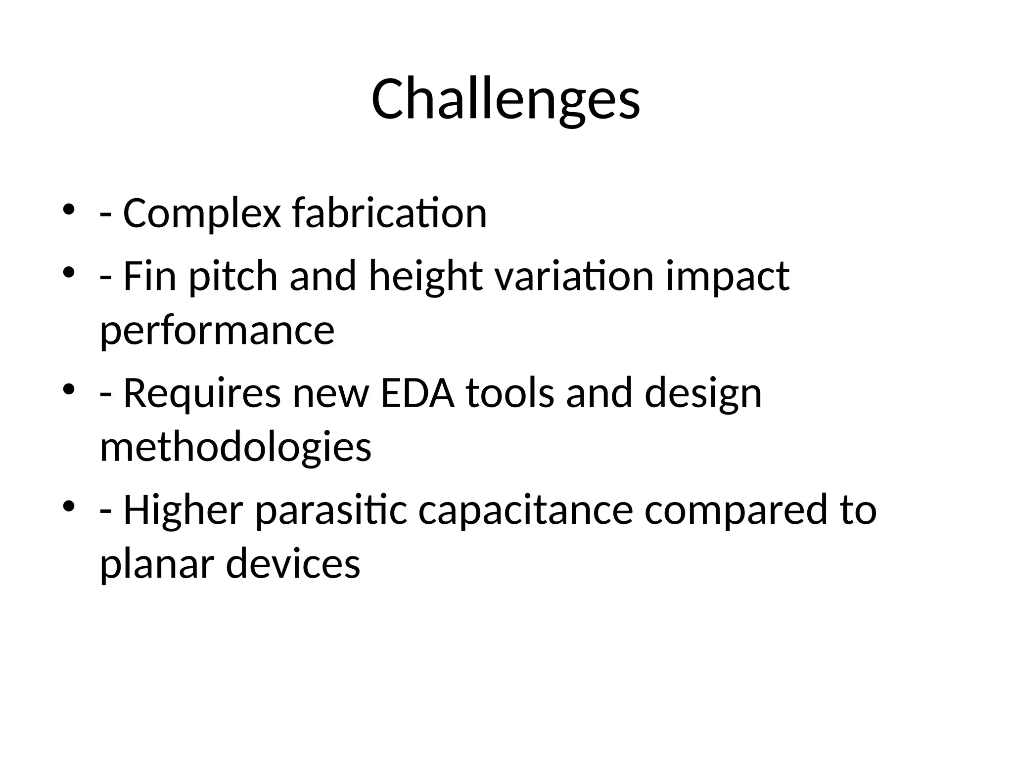
Challenges
• - Complexfabrication
• - Fin pitch and height variation impact
performance
• - Requires new EDA tools and design
methodologies
• - Higher parasitic capacitance compared to
planar devices
10.
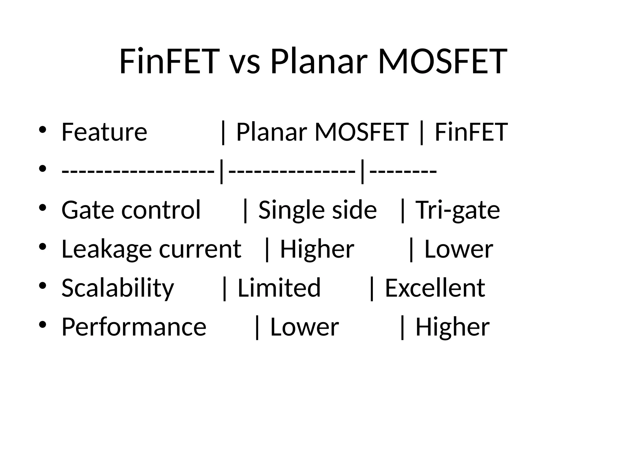
FinFET vs PlanarMOSFET
• Feature | Planar MOSFET | FinFET
• ------------------|---------------|--------
• Gate control | Single side | Tri-gate
• Leakage current | Higher | Lower
• Scalability | Limited | Excellent
• Performance | Lower | Higher
11.
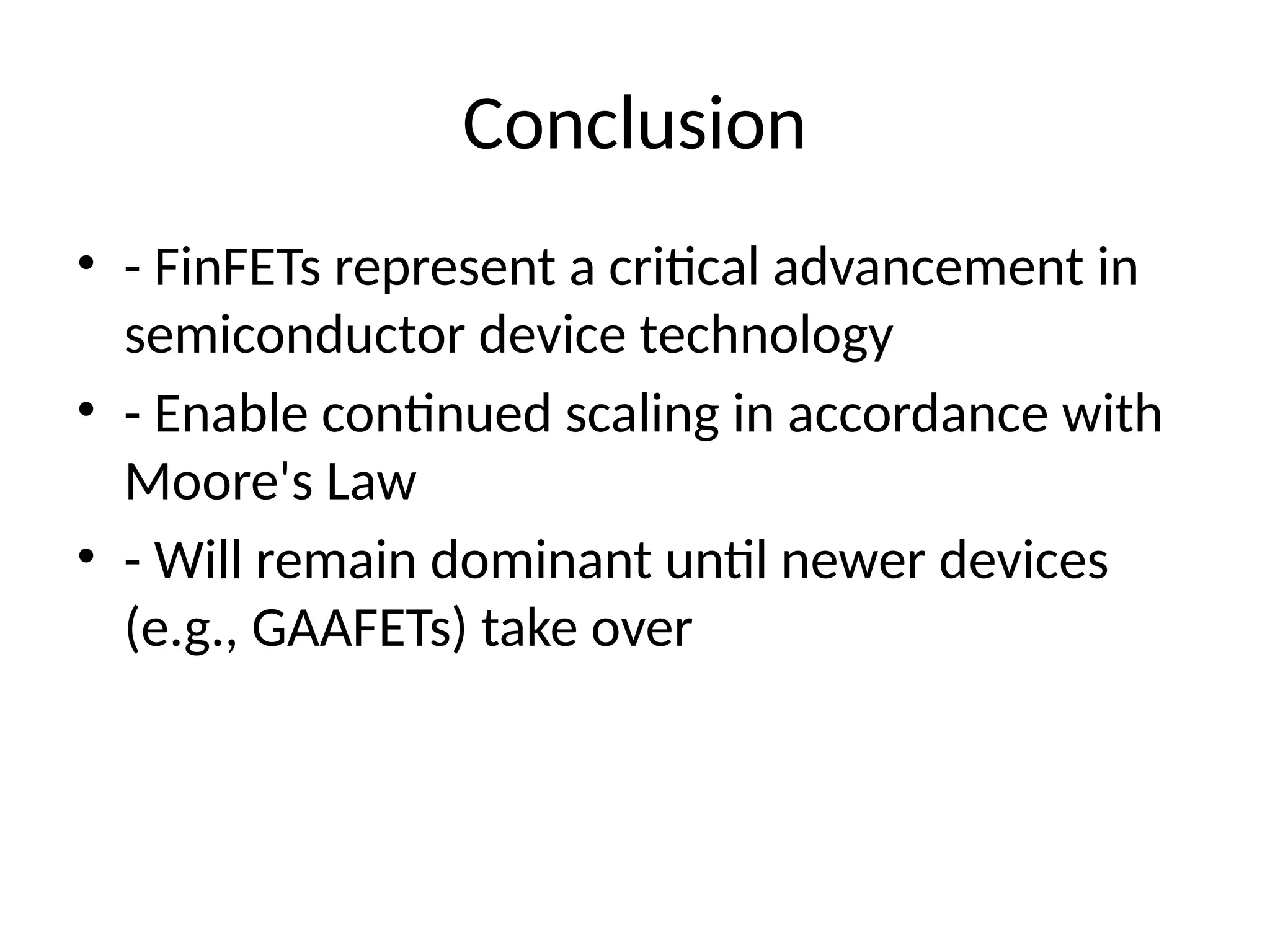
Conclusion
• - FinFETsrepresent a critical advancement in
semiconductor device technology
• - Enable continued scaling in accordance with
Moore's Law
• - Will remain dominant until newer devices
(e.g., GAAFETs) take over
12.
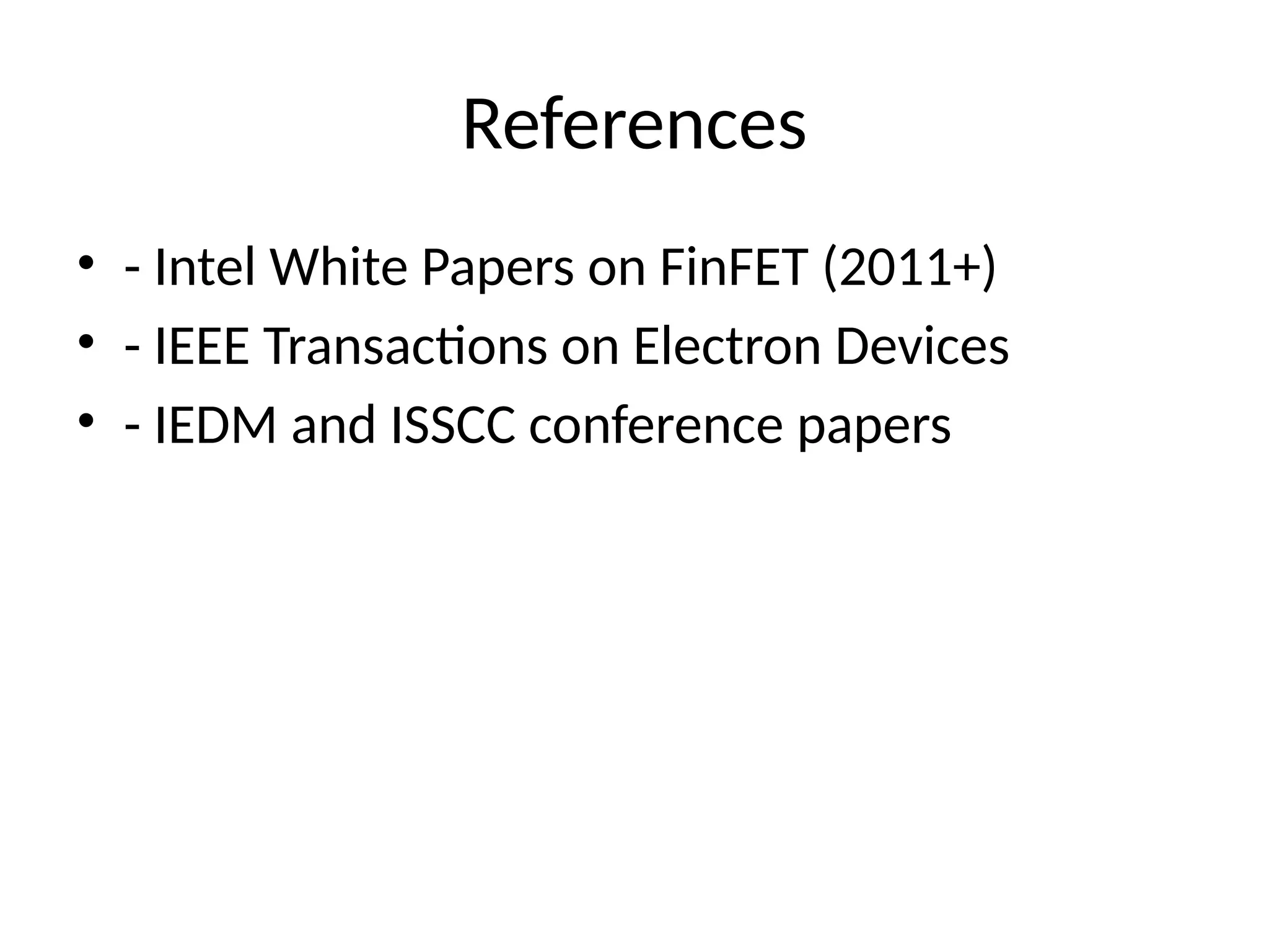
References
• - IntelWhite Papers on FinFET (2011+)
• - IEEE Transactions on Electron Devices
• - IEDM and ISSCC conference papers