Download as PDF, PPTX

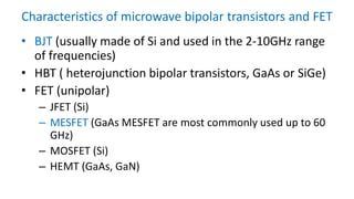
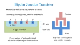


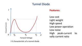


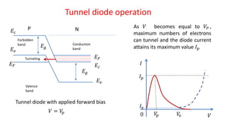


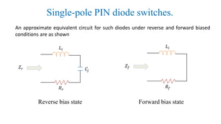


Microwave semiconductor devices include transistors, diodes, and detectors used in microwave systems. Bipolar junction transistors (BJTs) and field effect transistors (FETs) like MESFETs are commonly used in microwave applications. Schottky diodes have lower capacitance than PN junction diodes, making them suitable for microwave frequencies. Tunnel diodes exhibit negative resistance, allowing their use in microwave oscillators. PIN diodes have an intrinsic region that reduces junction capacitance. These devices are used in microwave systems for applications like amplification, mixing, and detection.