Downloaded 152 times

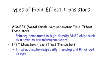
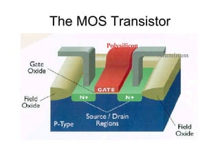
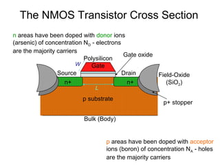
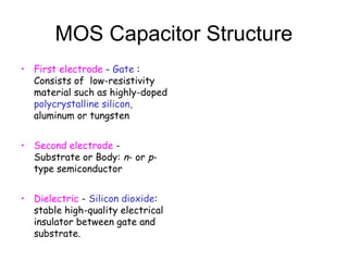
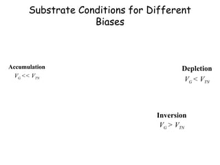
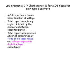


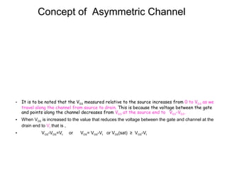
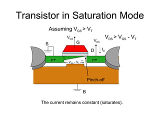
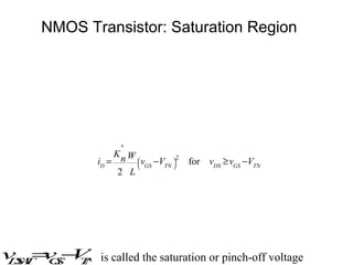
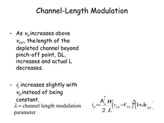


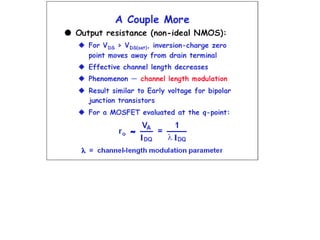

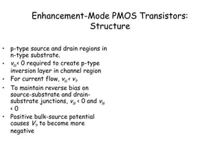


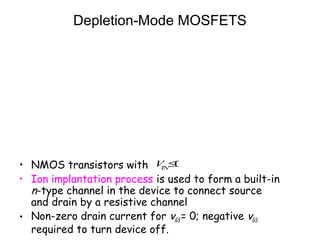


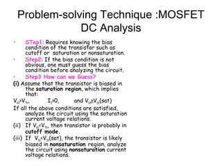
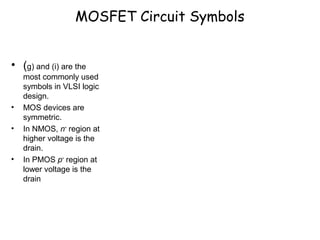
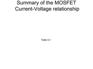

This chapter describes field-effect transistors (FETs), specifically MOSFETs and JFETs. It defines the key characteristics and operating regions of MOSFETs, including cutoff, triode, and saturation regions. Mathematical models are introduced for the current-voltage characteristics of MOSFETs and JFETs. The chapter also contrasts enhancement-mode and depletion-mode MOSFETs, defines symbols used in schematics, and explores biasing transistors and circuit analysis using MOSFET models.


