Download as PDF, PPTX

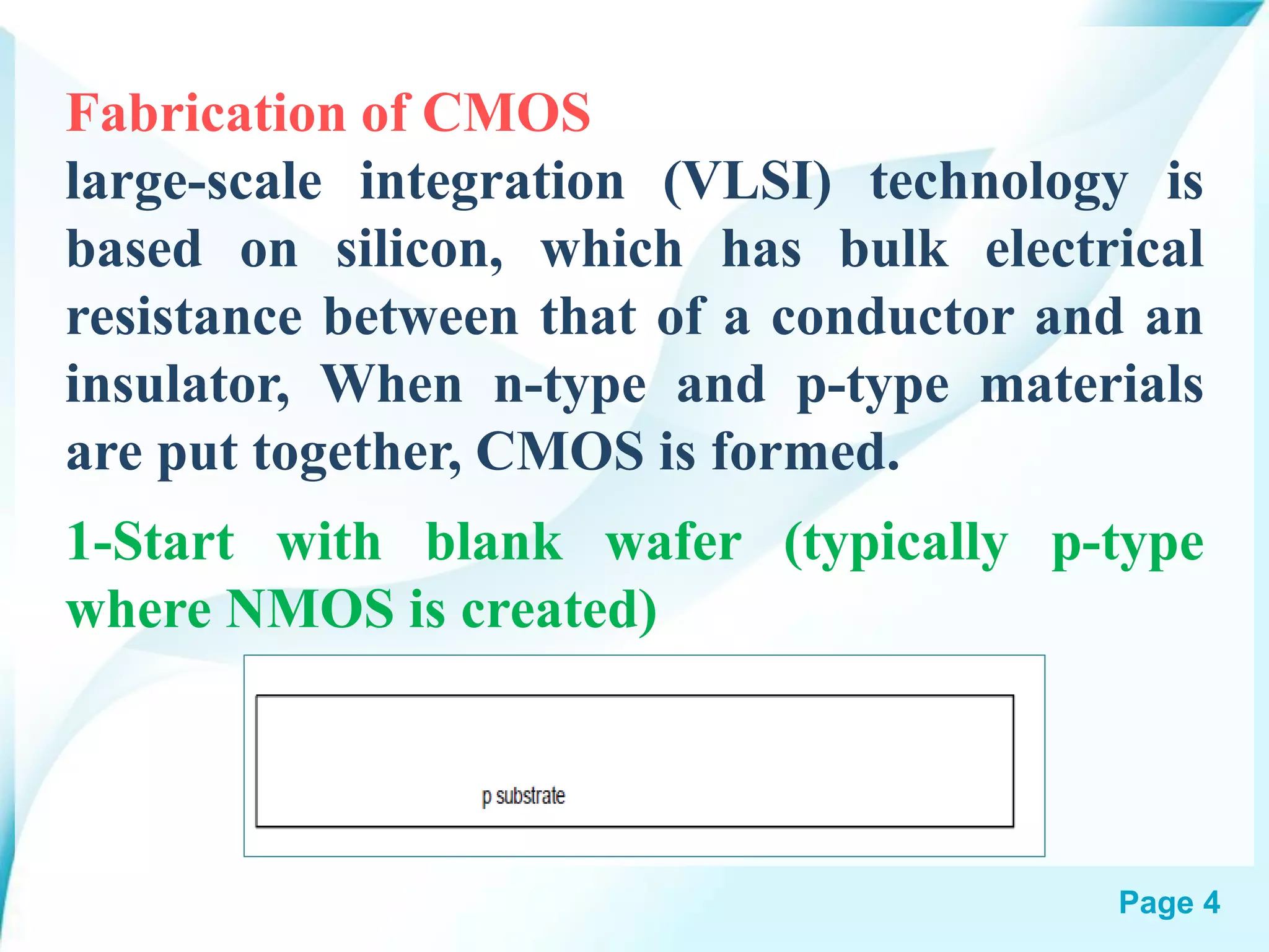
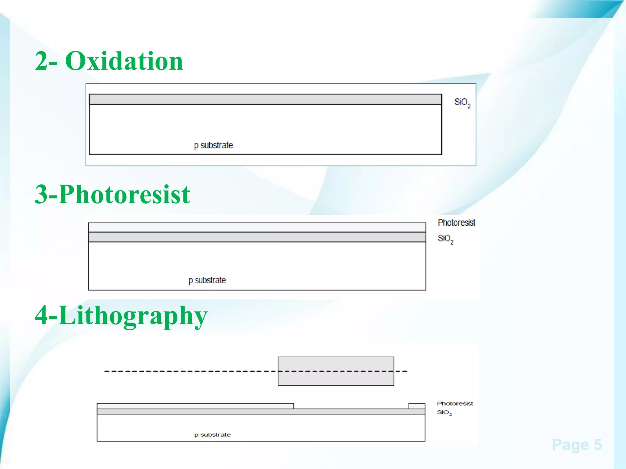
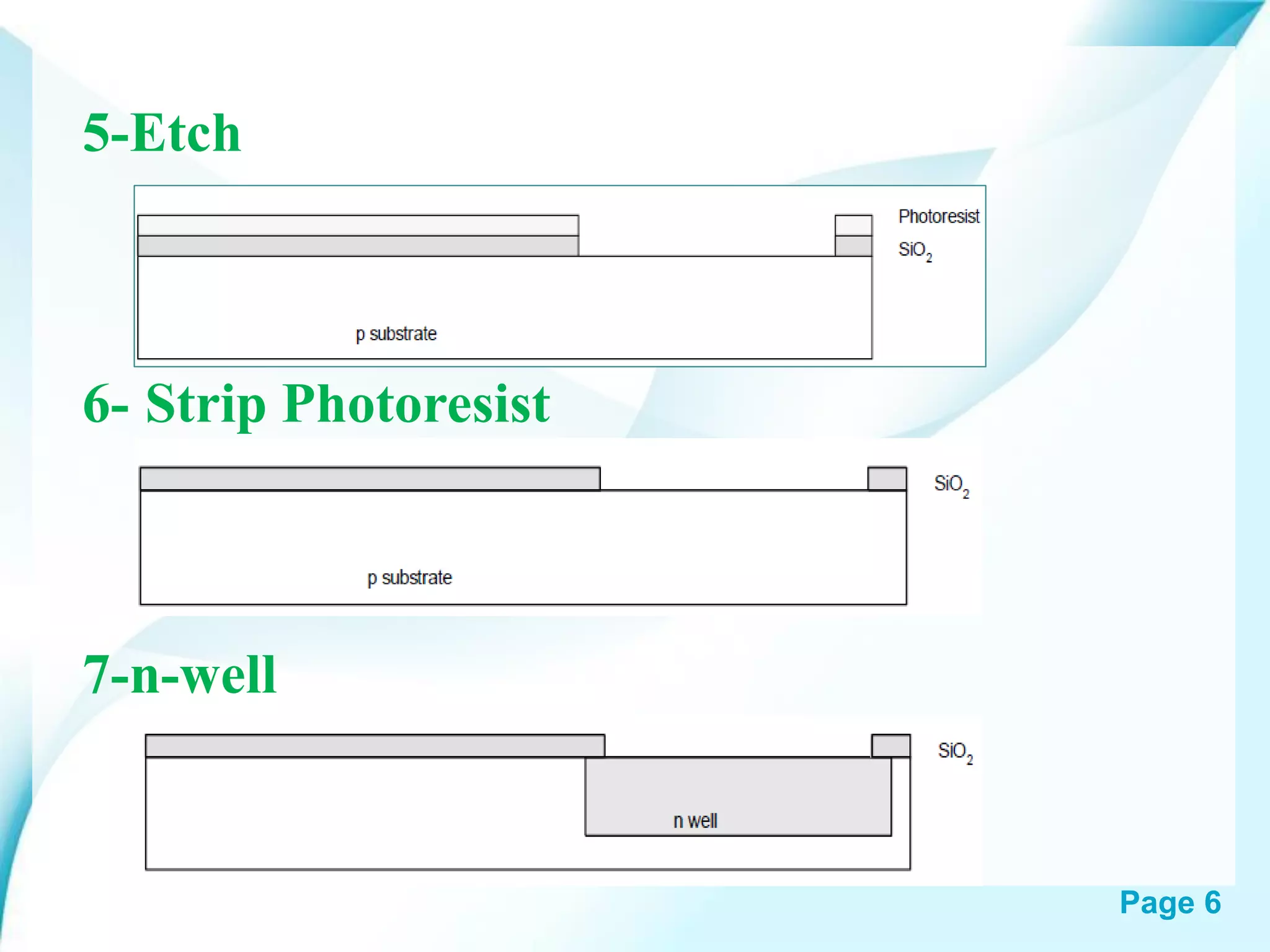
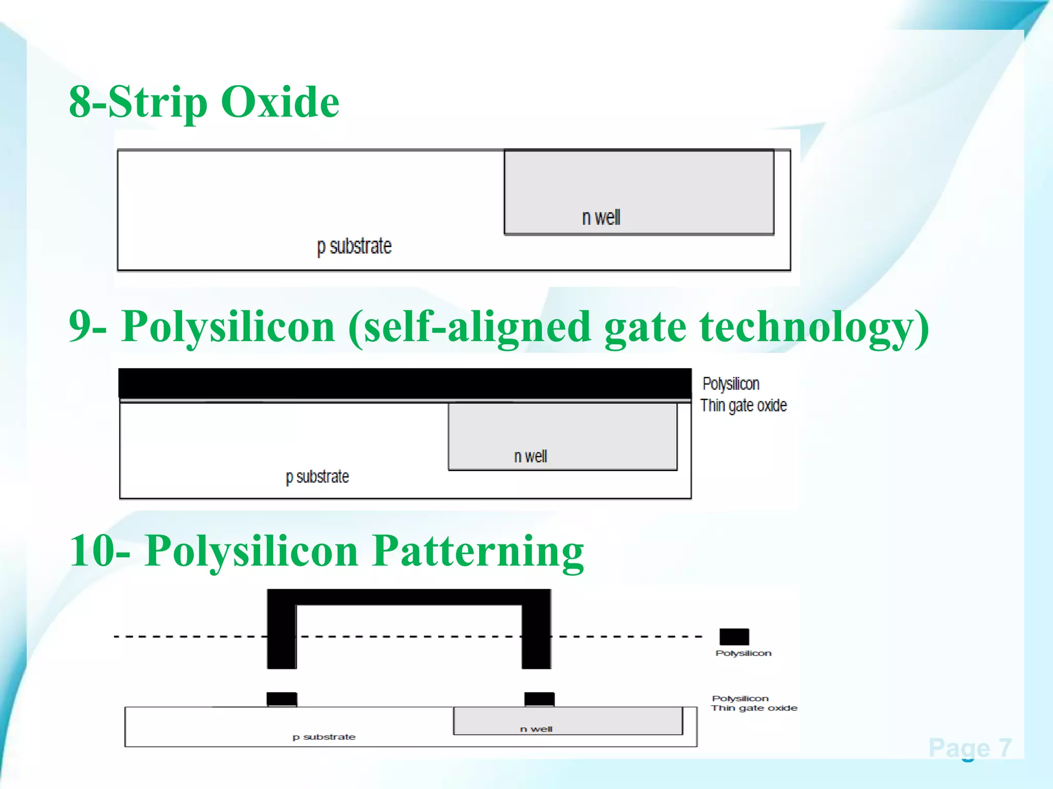
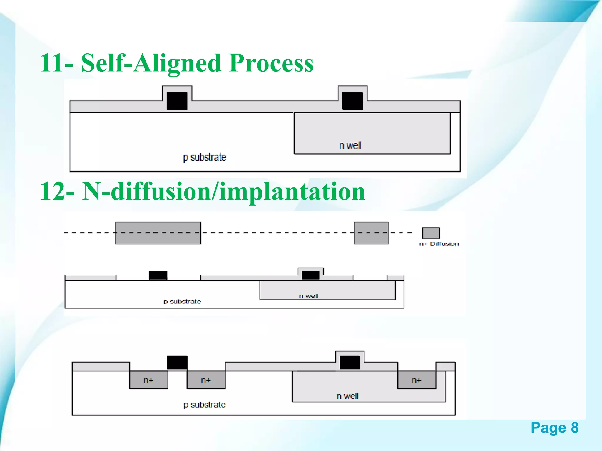
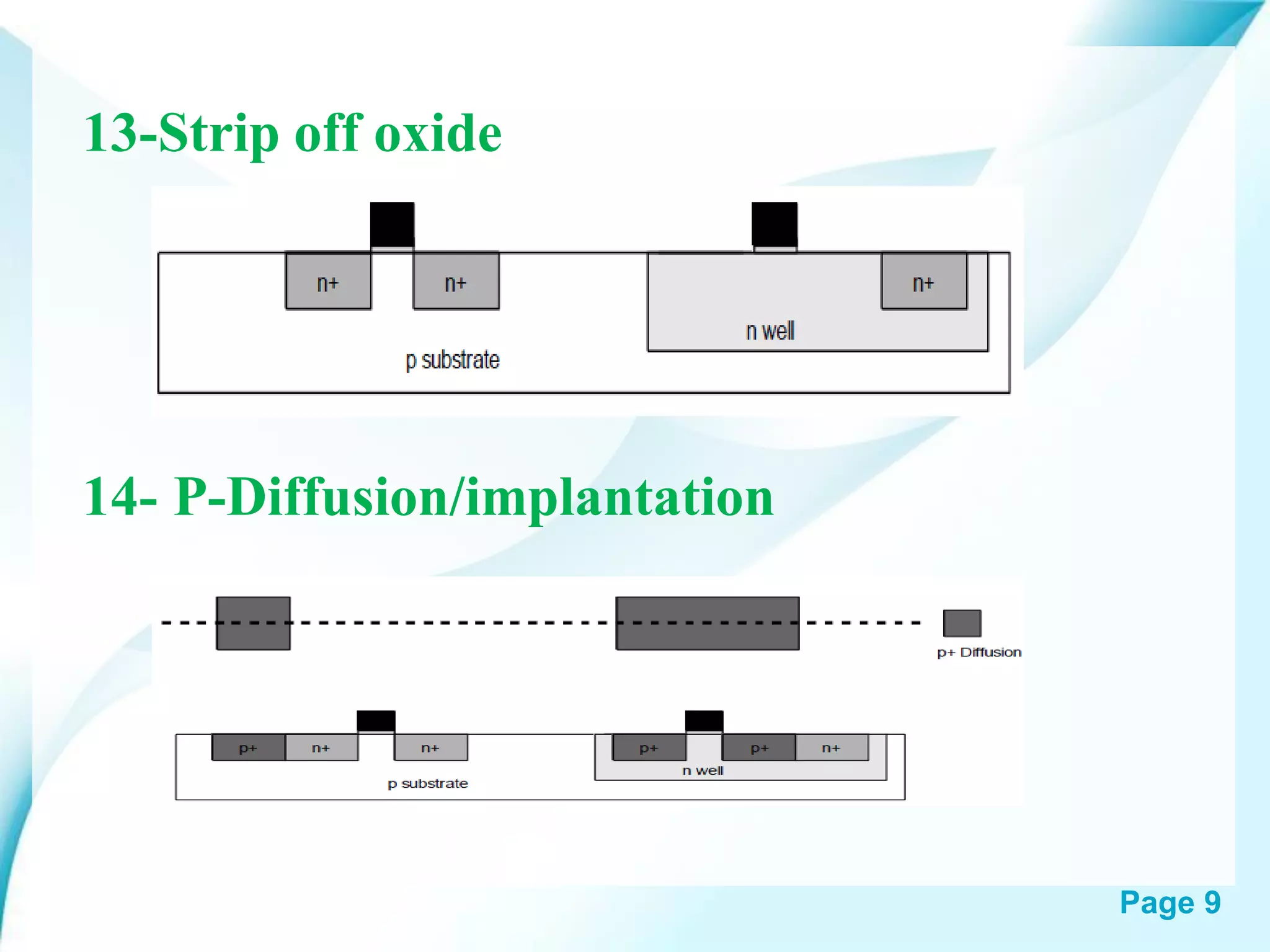
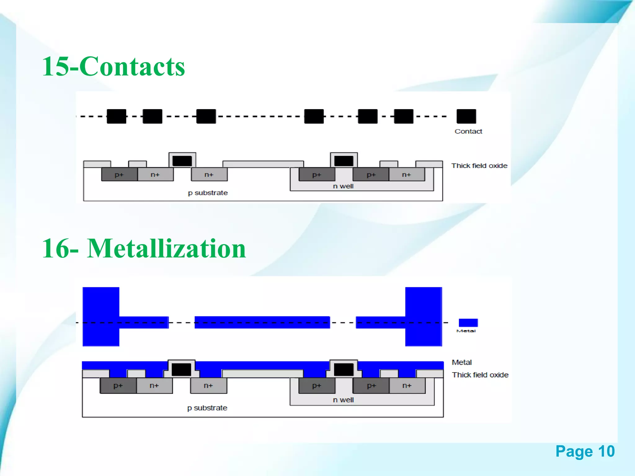
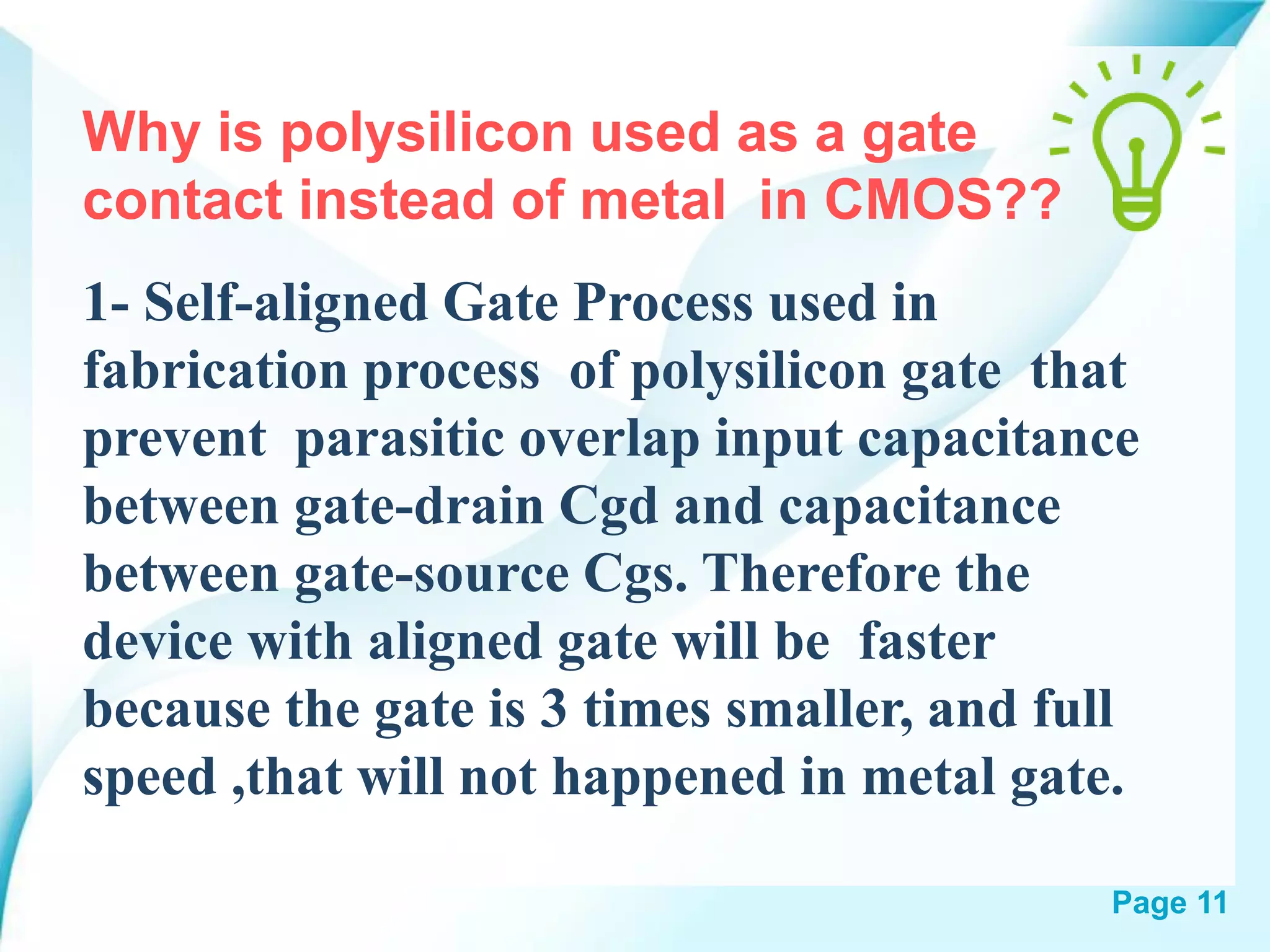
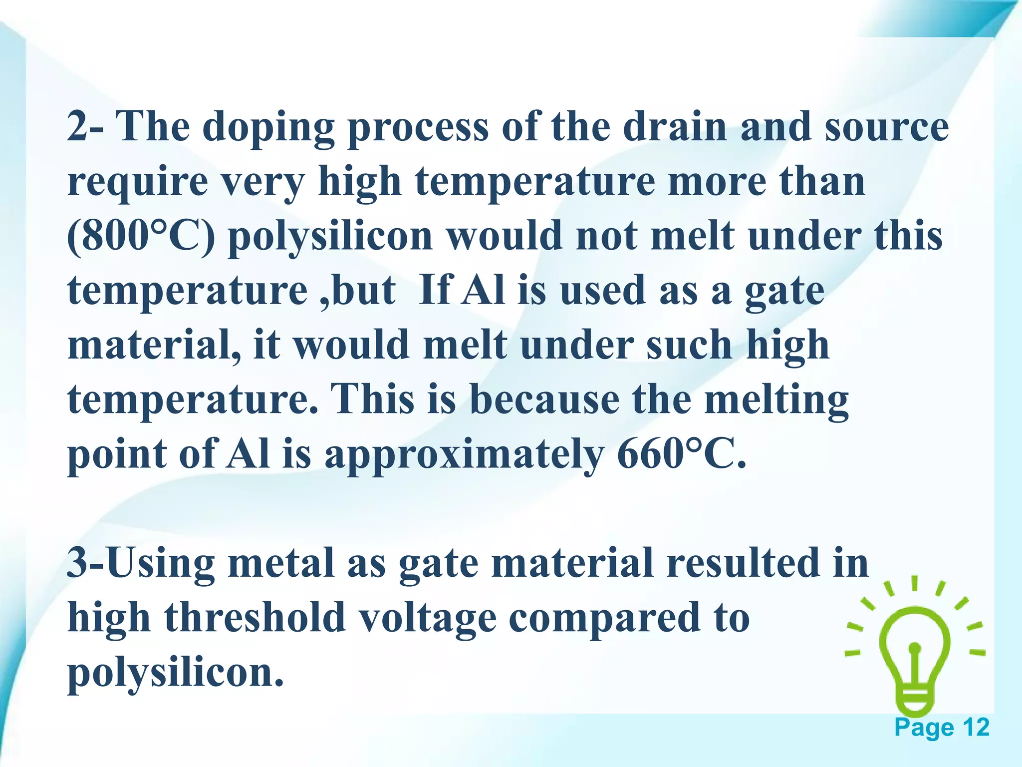
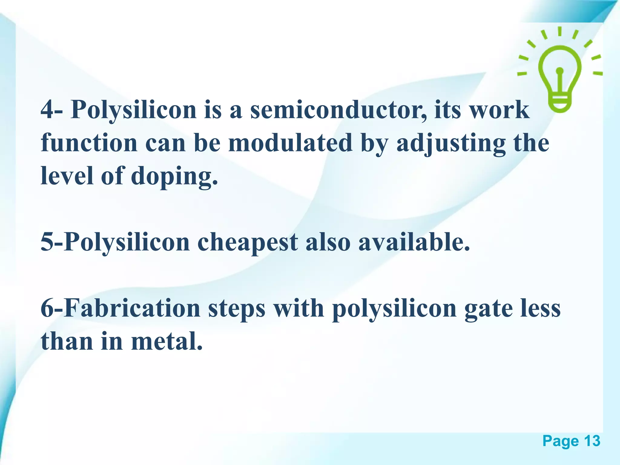

The document discusses the use of polysilicon as a gate contact in CMOS technology, detailing its advantages over metal, including lower threshold voltage, higher thermal resistance, and the ability to achieve a self-aligned gate process. It highlights the fabrication steps of CMOS technology and emphasizes the efficiency, low power consumption, and ease of integration in various digital and analog applications. Polysilicon's properties, such as modifiable work function through doping and lower fabrication complexity, make it a preferable choice in VLSI chip design.


