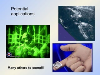
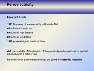
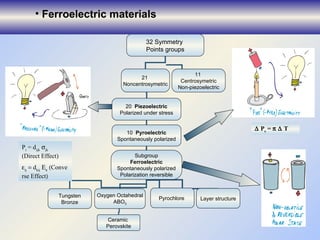
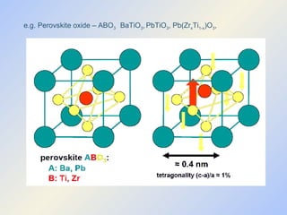
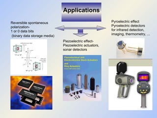
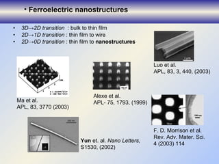
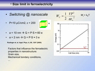
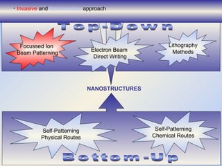
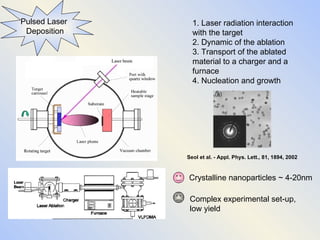
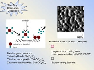
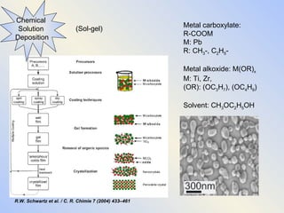
This document discusses ferroelectric nanostructures and their processing issues. It covers several topics including important events in the history of ferroelectricity, factors that influence ferroelectric properties at the nanoscale, and different invasive and non-invasive approaches for processing ferroelectric nanostructures such as top-down methods like focused ion beam patterning and bottom-up methods like self-assembly. Potential applications of ferroelectric nanostructures are also mentioned, including data storage, piezoelectric actuators, and pyroelectric detectors.
This is a power point presentation of project work on preparing Zinc oxide thin films by using SILAR technique and CBD technique and studying its characteristics.
Basics of Electrochemical Impedance SpectroscopyGamryInstruments
An introduction to Electrochemical Impedance Spectroscopy (EIS) theory and has been kept as free from mathematics and electrical theory as possible. If you still find the material presented here difficult to understand, don't stop reading. You will get useful information from this application note, even if you don't follow all of the discussions.
This presentation reviews the following paper.
Giannini, Vincenzo, Antonio I. Fernández-Domínguez, Susannah C. Heck, and Stefan A. Maier. "Plasmonic nanoantennas: fundamentals and their use in controlling the radiative properties of nanoemitters." Chemical reviews 111, no. 6 (2011): 3888-3912.
Basic of semiconductors and optical propertiesKamran Ansari
This presentation explains the band structure, intrinsic semiconductor, extrinsic semiconductor, electrical conductivity, mobility, hall effect, p-n junction diode, tunnel diode and optical properties of the semiconductor.
The present article gives the fundamental properties magnetism, different materials, properties of different magnetic materials like, dia,para and ferro magnetic materials. The notes also explain how magnetism appear in materials, type of magnets and brief applications of magnetic materials. The materials is best for undergraduate science and engineering students and any other people of interest in magnetism
Piezoelectricity is not a new concept but its application in recent instrumentation and daily life field is noticeable. i have prepared this report for enhancing and making the new technologies and applications about piezoelectronics known among readers. Don't forget to give feedback
In an age where every teeny tiny bit of electricity is valued, conservation is much talked about, can piezoelectricity be the messiah to ease the burden off the conventional energy sources?
Who says it cannot?
--
Presentation as a part of seminar coursework.
Power generation in footsteps by Piezoelectric materialsMelwin Dmello
Power generation in footsteps by piezo electric transducers - A project work by students of Alva's institute of engineering and technology, Moodbidre, Mangalore....
Slides created by Melwin Dmello... (ph; 8147814891)
An insight into the E-Passport, aka Biometric Passport, the need for biometrics in travel documents, the ICAO regulations governing the information contained in the electronic chip, RFID technique, Privacy threats in the current design.
Microstructural and Dielectric Characterization of Sr doped Ba(Fe0.5Ta0.5)O3 ...theijes
Solid state reaction method was used to synthesize Ba1-xSrx(Fe0.5Ta0.5)O3 ceramic(x=0, 0.1, 0.2, 0.3, 0.4 and 0.5). The raw materials of making Sr doped Ba(Fe0.5Ta0.5)O3 were BaCO3, SrCO3, Fe2O3, Ta2O5 (purity better than 99%). Pellet and ring shaped samples prepared from each composition were sintered at 1400 and 1450ºC for 5 hour. The phase formation of Ba1-xSrx(Fe0.5Ta0.5)O3 was checked using X-ray diffraction (XRD) technique and observed a cubic perovskite crystal structure in space group Pm3m (221). Microstructure of the individual compound was examined by the field emission scanning electron micrograph (FESEM). Grain size was found to be varied with Sr content. The lattice parameter decreased with increasing Sr content. Dielectric spectroscopy was applied to investigate the electrical properties of BSFT at room temperature and in a frequency range of 100Hz–100 MHz. An analysis of the dielectric constant εʹ and loss tangent tan with frequency was performed assuming a distribution of relaxation times. The low frequency dielectric dispersion corresponds to the DC electrical conductivity.
Introduction to nanoscience and nanotechnologyaimanmukhtar1
Introduction of nanoscience/nanotechnology ,properties/potential applications of nanomaterials and electrodeposition of metal single component and alloy nanowires in AAO template
A study of micro structural, magnetic and electrical properties of La-Co-Sm n...IJECEIAES
A Lanthanum (La 3+ ) doped Samarium-Cobalt nanoferrites (La_x,Co_0.2,Sm_0.2,Fe_(2-x) O_4, where x=0.0,0.5,1.0) have been synthesized by sol-gel method in citrate media. Obtained spinal ferrites micro structure properties have been investigated by XRD, FTIR, SEM-EDX, and TEM-SAED techniques. All the samples are nano in size with significant hysteresis. Micro structural analysis by XRD confirms the obtained samples showing the single phase cubic spinal structures with an average crystal size found from 12 nm to 25 nm, while the average particles sizes identified from TEM analysis are ranging from 21.5nm-26.8 nm (~23.4nm) and from 20.5 nm to 28(~26.4nm) nm for x=0.5,1.0. The lattice parameter found to be a= 8.402, 8.423, 8.467Å for the respective values of x= 0.0, 0.05, and 1.0. Electrical properties show increase in dc resistivity with increase in La ion concentration. Finally, it was concluded that the doping of Lanthanum ion (La 3+ ) in the ferrites structure is found to influencing the structural and electrical properties without scarifying the ferromagnetic character.
Study of highly broadening Photonic band gaps extension in one-dimensional Me...IOSR Journals
In this paper, we show theoretically that the reflectance spectra of one dimensional multilayer metal-organic periodic structure (1D MOPS) can be enhanced due to the addition of the organic constituents. We have used simple transfer matrix method to calculate the absorption, transmittance and reflectance of the 1D MOPS systems. The organic component like N,N’-bis-(1-naphthyl)-N,N’diphenyl-1; 1biphenyl-4; 4diamine (NPB) absorbs the light in ultra-violet, visible and infrared electromagnetic region and the structure with Ag-metal also having the tendency to absorb the light by the plasmaonic action and their refractive can be calculated from Drude equation. The reflectance spectra of multilayer 1D MOPS containing a variable number periodic of Ag/N,N’-bis-(1-naphthyl)-N,N’diphenyl-1; 1biphenyl-4; 4diamine (NPB) structure are calculated taking optical constant of NPB and Ag. The optical band gap and reflectance spectra of 1D MOPS of the considered structure is obtained in the visible and near infrared regions either with the variation of the metal layer thickness or thickness of the organic layer. From the results under investigation through TMM, tunability in the optical band gap was observed either change in thickness of the other layer 1/ or 2 or the angle of the incident. Due to optical absorption of the light in the different region of electromagnetic spectrum due to either N,N’-bis-(1-naphthyl)-N,N’diphenyl-1; 1biphenyl-4; 4diamine (NPB) or silver metal, the optical band gap of 1DMOPS shows the shift of band edges of λL and λR from ultra-violet to visible and the infrared with change the optical constant.
IMPROVEMENT IN MORPHOLOGICAL AND ELECTRO-MAGNETIC BEHAVIOUR OF HARD FERRITE P...Editor IJMTER
The Ni-Ir substituted strontium ferrite of Sr(Ni-Ir)xFe12-2xO19 (x = 0.02 & 0.08) were
synthesized by sol-gel auto combustion technique and characterized using X-ray diffraction (XRD),
Transmission Electron Microscopy (TEM) for morphological behaviour with electrical
characteristics using Impedance Analyzer. XRD results confirmed the formation of a single phase
M-type hexagonal unit cell of space group P63/mmc. The increase in Ni-Ir concentration increases
the lattice parameter. TEM analysis of the sample demonstrates the formation of nano-size particles
which decreases with substitution. In this paper we reported the variation of dielectric constant,
dielectric loss, tangent loss, conductivity and magnetic behaviour with composition with temperature
and frequency analysis of the sample. The migration of Fe3+ ion from octahedral to tetrahedral site
decreases the dielectric constant with increase in Ni-Ir concentration. Activation energies were
found similar with calculated at ferromagnetic and paramagnetic region. The material study we
confined that the activation energy in the paramagnetic region is higher than that in the
ferromagnetic region. The enhanced resistivity of Ni-Ir substituted strontium hexaferrites is a
prospective application in high frequency and in microwave devices development.
Synthesis and charaterization of la1 x srxmno3 perovskite nanoparticlesMai Trần
In recent times perovskite materials are extensively studied and have attracted much attention because they exhibit interesting the properties, showing potential applications in commercial, technical and biomedical. In Vietnam, perovskite materials be of interest research and applications are strong but with major research direction is to go deep into the electrical properties and the magnetic properties. The Lanthanum Strontium manganite is a perovskite-based crystal-structured ceramic material with the formula of La1-xSrxMnO3, where x describes the doping ratio. It has attracted much attention due to its good magnetic, electrical, and catalytic properties and is becoming an attractive possibility material in several biomedical applications, particularly with nano-size. In industry, this material is commonly used in as a cathode material in commercially produced solid oxide fuel cells. In this thesis, we present the Perovskite nanoparticles La1-xSrxMnO3 were successfully synthesized of the nanosize La1-xSrxMnO3 at x = 0; 0.1; 0.2; 0.3 and 0.4 which prepared by a modified sol-gel method. Structure and magnetic properties of them were systematically investigated in dependence on doped Sr ratio x. The structure was investigated by XRD and show slightly changed but magnetic properties varied strongly with changing the doping ratio x. Magnetic properties of samples were studied by Vibrating Sample Mode of Physical Properties Measurement System show at the room temperature, the samples show superparamagnetic properties with high saturated magnetization MS of 57 emu/g which strongly dependents on the doped Sr ratio x.
Lecture on Introduction of Semiconductor at North South University as the undergraduate course (ETE411)
=======================
Dr. Mashiur Rahman
Assistant Professor
Dept. of Electrical Engineering and Computer Science
North South University, Dhaka, Bangladesh
http://mashiur.biggani.org
2024.06.01 Introducing a competency framework for languag learning materials ...Sandy Millin
http://sandymillin.wordpress.com/iateflwebinar2024
Published classroom materials form the basis of syllabuses, drive teacher professional development, and have a potentially huge influence on learners, teachers and education systems. All teachers also create their own materials, whether a few sentences on a blackboard, a highly-structured fully-realised online course, or anything in between. Despite this, the knowledge and skills needed to create effective language learning materials are rarely part of teacher training, and are mostly learnt by trial and error.
Knowledge and skills frameworks, generally called competency frameworks, for ELT teachers, trainers and managers have existed for a few years now. However, until I created one for my MA dissertation, there wasn’t one drawing together what we need to know and do to be able to effectively produce language learning materials.
This webinar will introduce you to my framework, highlighting the key competencies I identified from my research. It will also show how anybody involved in language teaching (any language, not just English!), teacher training, managing schools or developing language learning materials can benefit from using the framework.
Introduction to AI for Nonprofits with Tapp NetworkTechSoup
Dive into the world of AI! Experts Jon Hill and Tareq Monaur will guide you through AI's role in enhancing nonprofit websites and basic marketing strategies, making it easy to understand and apply.
How to Make a Field invisible in Odoo 17Celine George
It is possible to hide or invisible some fields in odoo. Commonly using “invisible” attribute in the field definition to invisible the fields. This slide will show how to make a field invisible in odoo 17.
Macroeconomics- Movie Location
This will be used as part of your Personal Professional Portfolio once graded.
Objective:
Prepare a presentation or a paper using research, basic comparative analysis, data organization and application of economic information. You will make an informed assessment of an economic climate outside of the United States to accomplish an entertainment industry objective.
Safalta Digital marketing institute in Noida, provide complete applications that encompass a huge range of virtual advertising and marketing additives, which includes search engine optimization, virtual communication advertising, pay-per-click on marketing, content material advertising, internet analytics, and greater. These university courses are designed for students who possess a comprehensive understanding of virtual marketing strategies and attributes.Safalta Digital Marketing Institute in Noida is a first choice for young individuals or students who are looking to start their careers in the field of digital advertising. The institute gives specialized courses designed and certification.
for beginners, providing thorough training in areas such as SEO, digital communication marketing, and PPC training in Noida. After finishing the program, students receive the certifications recognised by top different universitie, setting a strong foundation for a successful career in digital marketing.
Acetabularia Information For Class 9 .docxvaibhavrinwa19
Acetabularia acetabulum is a single-celled green alga that in its vegetative state is morphologically differentiated into a basal rhizoid and an axially elongated stalk, which bears whorls of branching hairs. The single diploid nucleus resides in the rhizoid.
Biological screening of herbal drugs: Introduction and Need for
Phyto-Pharmacological Screening, New Strategies for evaluating
Natural Products, In vitro evaluation techniques for Antioxidants, Antimicrobial and Anticancer drugs. In vivo evaluation techniques
for Anti-inflammatory, Antiulcer, Anticancer, Wound healing, Antidiabetic, Hepatoprotective, Cardio protective, Diuretics and
Antifertility, Toxicity studies as per OECD guidelines
A Strategic Approach: GenAI in EducationPeter Windle
Artificial Intelligence (AI) technologies such as Generative AI, Image Generators and Large Language Models have had a dramatic impact on teaching, learning and assessment over the past 18 months. The most immediate threat AI posed was to Academic Integrity with Higher Education Institutes (HEIs) focusing their efforts on combating the use of GenAI in assessment. Guidelines were developed for staff and students, policies put in place too. Innovative educators have forged paths in the use of Generative AI for teaching, learning and assessments leading to pockets of transformation springing up across HEIs, often with little or no top-down guidance, support or direction.
This Gasta posits a strategic approach to integrating AI into HEIs to prepare staff, students and the curriculum for an evolving world and workplace. We will highlight the advantages of working with these technologies beyond the realm of teaching, learning and assessment by considering prompt engineering skills, industry impact, curriculum changes, and the need for staff upskilling. In contrast, not engaging strategically with Generative AI poses risks, including falling behind peers, missed opportunities and failing to ensure our graduates remain employable. The rapid evolution of AI technologies necessitates a proactive and strategic approach if we are to remain relevant.
Normal Labour/ Stages of Labour/ Mechanism of LabourWasim Ak
Normal labor is also termed spontaneous labor, defined as the natural physiological process through which the fetus, placenta, and membranes are expelled from the uterus through the birth canal at term (37 to 42 weeks
Synthetic Fiber Construction in lab .pptxPavel ( NSTU)
Synthetic fiber production is a fascinating and complex field that blends chemistry, engineering, and environmental science. By understanding these aspects, students can gain a comprehensive view of synthetic fiber production, its impact on society and the environment, and the potential for future innovations. Synthetic fibers play a crucial role in modern society, impacting various aspects of daily life, industry, and the environment. ynthetic fibers are integral to modern life, offering a range of benefits from cost-effectiveness and versatility to innovative applications and performance characteristics. While they pose environmental challenges, ongoing research and development aim to create more sustainable and eco-friendly alternatives. Understanding the importance of synthetic fibers helps in appreciating their role in the economy, industry, and daily life, while also emphasizing the need for sustainable practices and innovation.
14. Pulsed Laser Deposition 1. Laser radiation interaction with the target 2. Dynamic of the ablation 3. Transport of the ablated material to a charger and a furnace 4. Nucleation and growth Seol et al. - Appl. Phys. Lett., 81, 1894, 2002 Crystalline nanoparticles ~ 4-20nm Complex experimental set-up, low yield
15. Met.Org. Chem.Vap. Deposition Large surface coating area Used in combination with FIB, EBDW Expensive equipement Metal organic precursor: Tetraethyl lead - Pb(C 2 H 5 ) 4 Titanium isopropoxide: Ti(i-OC 3 H 7 ) 4 Zirconium tert-butoxide: Zr (t-OC 4 H 9 ) 4 M. Shimizu et.al.-Jpn. J. Apl. Phys, 33, 5168 (1994)
16. R.W. Schwartz et al. / C. R. Chimie 7 (2004) 433–461 Metal carboxylate: R-COOM M: Pb R: CH 3 -, C 2 H 5 - Metal alkoxide: M(OR) x M: Ti, Zr, ( OR ): (OC 3 H 7 ), (OC 4 H 9 ) Solvent: CH 3 OC 2 H 5 OH Chemical Solution Deposition (Sol-gel)
17. Self-Patterning Chemical Routes Pb(O 2 C 2 H 3 ) 2 R= [ H2O ]/ [Pb] Zr(OC 4 H 9 ) 4 pH=11 Ti(OC 4 H 9 ) 4 C 4 H 10 O BET: 58nm BET: 109nm BET: 144nm Cost-effective, various shapes Agglomeration (Sol-gel) 11 -PT- 15 11 -PZ- 15 11 - PZT- 15
18. Self-Patterning Chemical Routes Synthesis, Functionalization and surface treatment of Nanoparticles Marie-Isabelle Baraton/ ASP 2003 Alexe, Harnagea and Hesse, J. Electroceram. 12, 69 (2004) Microemulsion Removal of the surfactant Uniforme particles in nm range
Ferroelectricity is a phenomen on that was discovered in 1921 in Rochelle salt or sodium potasium tartrate. Certainly one of the major “turning points” in ferroelectricity came in the very early 1940s with discovery of the unusual dielectric properties of a number of simple mixed oxides which crystallize with the perovskite structure . The first of them was barium titanate Perhaps the most significant theoretical development in ferroelectricity occurred in 1960 with the formulation of the soft-mode description of the ferroelectric transition In 80-s the age of integration, in this time Capacitors, transducers, and electrooptic switches made from ferroelectric ceramics and crystals are being incorporated into thick-film and thin-film circuits, or multilayer packages. At present we are in the age of miniaturi zation.
All crystals that are found in nature can be devided into 32 different classes or point groups. These 32 point groups are subdivisions of 7 basic crystal system that are in order of ascending symetry: triclinic, monoclinic, orthorombic, tetragonal, rhombohedral, hexagonal and cubic. Of the 32 points groups, 21 classes are noncentrosymetric (a necesary condition for piezoelectricity to exist) and 20 of these are piezoelectric These crystal develop an electrical charge (polarization) under an applied mechanical stress this is called direct effect and a mechanical movement is generated by the application of an electrical field – converse effect . 10 crystal clases out of possible 20 are pyroelectric. This group of materials posses the unusual characteristic of beeing permanently polarized within a given temperature range. This polarization changes in the temperature gradient. A subgroup of spontaneously polarized pyroelectrics is a very special category of materials known as ferroelectrics. These materials posses spontaneous dipole which can be reversed by an electric field of some magnitude less than dielectric breakdown of the materials itself. some examples of such materials are tungsten bronze, Oxigen octahedral compounds with ABO3 stucture, the most known of them are ceramic perovskites. Other types are pyrochlore and layer structure generation of electricity as a result of mechanical pressure - direct effect mechanical distortion in response to a voltage applied across a piezoelectric material – inverse effect spontaneous polarization whose amplitude changes under the influence of temperature gradients reversible, non-volatile macroscopic spontaneous electric dipole moment in the absence of an external electric field.
Perovskite structure can be ideally described as a cubic unit cell with a large cation A as Ba, Pb ocupying the corner sites, a smaller cation B Ti, Zr in the body center and oxigen ocupying the centers of the faces. The cubic structure is the high tempeature stable form and it is paraelectric . On cooling down, at a certain temperature, called Curie temperature the symmetry of the crystal breaks down, and a tetrgonal distorsion takes place. The tetragonal form is a ferroelectric one and ferroelectricity originates from a small displacement of the transition metal cation from the centre of the O6 octahedron. This leads to a net dipole moment per unit volume called polarization. Almost all the ferroelectric perovskites contain non-magnetic transition metal ions with an empty d -shell ( d 0 confi guration), for example Ti4+, Nb5+ and W6+. Apparently the presence of the d 0 plays an important role in formation of a ferroelectric state.. In this way a stronger covalent bond with one (or three) instead of six weaker bonds with neighbouring oxygen atoms is formed.
Ferroelectrics find three main technological applications based on their physical characteristics: Because ferroelectric materials possess spontaneous polarization, when an electrical field is applied they present a non-linear response in polarization which is known as hysteresis. By changing the direction of the applied field polarization is also changed. Polarization up can be associated to 1 or 0 and polarization down can be 0 or 1. the two states are used in binary data storage: memory of the mobile phone, digital camera and so on. The ferroelectric materials are also piezoelectric. actuators are devices that produce a displacement or movement when voltage is applied. Actuators are used for many functions, including cancelling vibration, tool adjustment and control, micro-pumps, mirror positioning, wave generation, structural deformation, inspection systems and scanning microscopes. Another direction of applications is based on pyroelectric effect, for pyroelectric detectors for infrared detection, imaging, thermometry, ... .
in 1940-1950 bariun titanate era, the only known form to prepare materials was bulk a tri dimensional structure. In the age of integration, a new shape become available - by reducing one of the dimensions of the bulk . At this point we can talk about the transition from 3D to 2 D or from bulk to thin film. Portability of electronic systems has become a key driver of advanced semiconductor technologies. To meet the demand, new sophisticated materials and technologies are being introduced and reducing the size is required. This age of miniaturization is driven by the transition from 2D to one or zero D In other words, a ferroelectric nanostructure is a structure with all dimensions negligable!
Due to the technical evolution and industrial requirements about miniaturization, the scientist involve in the ferroelectric material research has believed that the ferroelectricity disappear at the moment when the polarization cannot be measured anymore. That limit was around 75-50nm. The ferroelectric polarization results from the sum over all dipol moments within a unit cell and it is equivalent to a surface charge density. Considering a ferroelectric matrerial with charactristic values for bulk P=10 and eps=200 for a capacitor with 100nm 2 there are aproximately 60electrons to swich and only three for the 4nm 2 capacitor. Applicability also requires two stable ferroelectric groundstates to toggle between. However, as we compare the energy W C of a ferroelectric capacitor with volume V : W C = 1 / 2 V P 2 /εε 0 2 with the thermal energy of k B T ( k B Boltzmann constant, T absolute temperature) at room temperature, it becomes evident that for the above values and small capacitors thermal fluctuations will become noticeable (1 nm3 corresponds to 17 meV). To assure a low thermally induced switching probability, W C should therefore be well above k B T .
How to build these structures? What methods are available? The first approaches at which scientists looked were those available in microelectronics. "Top down" implies a continuation of present technology, building devices that are smaller, faster, and less expensive by refining current fabrication methods. Increasing our knowledge of the chemical and physical properties of molecules such that we can design systems in which a desired pattern or product assembles itself. They are called self Paterning Physical and Chemical Routes and they are known as "Bottom up“ approach. Life, from single-celled animals to humans, is the inspiration for bottom-up approaches. Nanostructures obtained by top–down approach often suffer from damage by ion bombardment, which impedes the distinction between real size effects and those induced by the patterning method. Non-invasive techniques avoid these damages either by patterning prior to the final crystallization (e.g. e-beam direct writing or by bottomup approaches: self-assembly or by using suitable templates.
The FIB equipment is conceptually similar to a scanning electron microscope (SEM), but instead of a beam of electrons, a highly focussed beam of gallium ions is used to scan the sample surface. This ion beam can be used for two purposes: imaging, and micromachining: Scanning a low-current beam over an area of the sample surface and simultaneously collecting the induced secondary electrons, one can produce a high-resolution image of the sample, whereas at high beam current, highprecision local sputtering and milling can be easily performed. FIB equipment also allows the fabrication of small structures by direct deposition of metals (such as tungsten, gold, or platinum)which can be used as electrdes with a minimum feature size down to 40 nm and a precision of 20 nm, allowing studies on quantum transport mechanisms Having the unique nanopatterning ability to add or remove features, the FIB method is currently used to modify integrated circuits and masks, or to fabricate cross section transmission electron microscopy specimens. The major drawback of the method is associated with the high damage that occurs during milling and imaging, While most of the structural defects can be healed by a high-temperature thermal annealing after milling, a gallium doping is basically unavoidable and in special cases might be relatively harmful to the final electrical properties. A thermal annealing of the cut-out structures recovers the ferroelectric properties, but in general a damaged layer up to 10 nm thick still remains, in which the ferroelectric properties are altered The Focused Ion Beam (FIB) tool can cut away (mill) material from a defined area with dimensions typically in square microns or deposit material onto it. Milling is achieved by accelerating concentrated gallium ions to a specific site, which etches off any exposed material, leaving a very clean hole or surface. By introducing gases or an organic gas compound, the FIB can selectively etch one material much faster than surrounding materials, or deposit a metal or oxide. The FIB is used for such tasks as site-specific cross-sectioning for interfacial microstructure studies, preferential removal of certain metals or oxides, semiconductor device editing or modifications, site-specific TEM sample preparation, and grain imaging.
Electron Beam direct method is a non-invasive aproach. It starts from a solution containing metalorganic compounds or metal colloids. A substrate is spin-coated with a thin precursor film that contains the required elements in a proportion corresponding to that of the target ferroelectric phase. For example, precursor films for SBT and PZT structures can be prepared from Sr-, Bi-, and Pb-ethylhexanoate, Ti- and Zr-isopropylene, and Ta-methoxide solutions, using xylene and 2- methoxyethanol, respectively, as solvents. The obtained precursor film is dried and then patterned by scanning an electron beam of about 3 nm diameter over selected areas of the film (“pattern exposure”), and immersing the exposed sample for 1 minute in toluene (“pattern development”), followed by dry-blowing with nitrogen. As an example for EBDW, this fig. shows scanning electron microscope (SEM) images of PZT arrays
Lithography means printing Photolithography - is used in semiconductor device applications– it consists of producing a mask carrying the requisite pattern information and subsequently thansfering that pattern using some optical technique into a photoactive polymer or photoresist.In principle the resolution is limited by the optical system. to improve the resolution to nanometer range this requires the use of an electromagnetic radiation with a smaller wave length: extreme UV light or X-ray. A more friendly method is nanoimprint lithography (NIL). This does not use any energetic beam, so the resolution is not affected by the optical system The method has been adapted to chemical solution deposition (CSD) derived PZT precursor films to generate ferroelectric PZT cells down to 300 nm In this approach the deposited gel layer is patterned by imprinting a SiO2-Si mold into the film at a typical pressure of 1 kbar. After this process the imprinted gel layer is pyrolized and subsequently crystallized in air. The method enables a relatively low cost and large area patterning. In the case of polimers, the resolution of this method goes down to 20nm. However lateral ferroelectric nanostructures in the range of 20 nm as demonstrated for polymers have not been obtained.
There is a considerable interest in other fabrication methods that are not based on removing the material of the thin films, but rather on building structures from the bottom, using atoms and molecules. The bottom up approches will in principle allow inexpensive fabrication of structures with size of 10-20nm. The primary disadvantage of the bottom up methods is the random positioning of the obtained structures, that will make a precise interconection of them virtualy imposible. Self –patterning via physical routes seem to be reliable and making use of simple physical processes.
Pulsed laser deposition is a technique for creating thin films. Pulsed laser deposition (PLD) and pulsed laser ablation are also potential methods to obtain nanoparticles deposited on a substrate or in the form of a dispersed powder, The PLD method involves evaporation of a solid target in an Ultra High Vacuum chamber by means of short and high-energy laser pulses. In a typical PLD process, a ceramic called target is placed in a vacuum chamber. A pulsed laser beam vaporizes the surface of the target, and the vapor condenses on a substrate. The main components are a laser, optics, and a vacuum system. Additionaly for preparing nanoparticles a charger, a furnace and a collector are required. The principle of pulsed laser deposition, is a very complex physical phenomenon. It does not only involve the physical process of the laser-material interaction at the impact of high-power pulsed radiation on solid target, but also the formation of the plasma plume with high energetic species and even the transfer of the ablated material through the plasma plume onto the heated substrate surface. The particle formation process in PLD generally can be divided into the following four stages. The fig presents PZT nanoparticles obtained by laser ablation after heat tretment at 900 o C.
Chemical Vapor Deposition (CVD) is a chemical process for depositing thin films of various materials. In a typical CVD process the substrate is exposed to one or more volatile precursors, which react and/or decompose on the substrate surface to produce the desired deposit.When the volatile precursors are metal-organic precursors, such as ...The method is named MOCVD. Frequently, volatile by products are also produced, which are removed by gas flow through the reaction chamber.
This possibility of creating nanostructure has been found during an effort of growing single-crystal epitaxial films by chemical solution deposition (CSD). Lange, Speck, and coworkers have theoretically and experimentally established that an ultrathin amorphous layer of PZT (or another perovskite oxide) deposited onto a single-crystal substrate such as SrTiO3, during high-temperature crystallisation breaks up into small islands due to a microstructural instability. The driving force of this process is the minimisation of the free energy of the film-substrate system, by lowering the interface area (forming islands) and by forming low-energy surfaces via faceting The process starts with the preparation of suitable precursors that are often salts, typically, carboxylates, or other metallo-organic compounds, usually, alkoxides. The precursors are dissolved in appropriate solvents and mixed in a stoichiometric ratio that yields the desired composition of the final film. In some cases, additives such as chemical stabilizers are included during solution synthesis and additional processing steps, such as refluxing, are employed to adjust the properties of the coating solution. The next processing step is deposition of the coating solution on the substrate by spin coating using a rotating substrate, spray coating the misted solution, or dip coating the substrate in a solution bath. Subsequently, the (wet) as-deposited film is dried, pyrolyzed, crystallized, and (optionally) post-annealed for further densification or microstructure manipulation.
Using simple chemistry it is possible to fabricate nanosize crystals or nanoparticles which can later be spead onto any substrate surface. Very simillar to the method described before, particles with sizes in nanometer range can be prepared . The starting materials are, lead acetate which is a metal carboxylate, zirconium end titanium butoxide which are metal alkoxide and butanol (parent alcohol ) as solvent. Similar as befor they are mixed, refluxed and by products are removed. in this approch water is added to hydrolyse the alkoxide groups and imediately a gel is formed. After drying this leads to a very fine powder .
A microemulsion is defined as a dispersion of two immiscible liquids consisting of microdomains of one or both liquids stabilized by an artificial film of surface active molecules (surfactant). The water in oil (W/O) type of emulsion is formed from water droplets (5-25nm) which are dispersed in the oil phase. If two reactants A and B in the water phase of two different microemulsions are mixed,, reactants A and B are exchanged between the water droplets because of collision and coalescence. This interchange is very fast. As the reactants come in contact with each other, they react and form precipitate AB. The nucleation of the precipitate particles takes place inside the water droplets. The final particle size is controlled by the size of the water droplets, which in turn is controlled by the ratio of water to surfactant. When the size of the particles becomes comparable to the droplet size, the surfactant molecules are atached to the surface of the particles, stabilizing and protecting them against further growth.
Due to their small size, the characterisation of the cells or structures obtained cannot be achieved using conventional measurement techniques. For this purpose, scanning probe techniques, in particular scanning force microscopy (SFM), have proven to be most valuable. The principle of an SFM is quite simple and it is very similar to AFM. A sharp tip mounted on a cantilever is brought close to the sample surface. The (attractive or repulsive) force between the tip and the surface is detected using the bending of the cantilever. A feedback loop adjusts the z-position of the cantilever using a piezoelectric element, so that the interaction force is kept constant. By scanning the tip over the surface and recording the z-position of the cantilever, a map of the sample topography can be obtained . In the case of PFM a conductive tip is brought into contact with the with the surface and by applying an electrical field the piezoelectric response is detected. The fig presents three possible orientations of the polarization and electrical field. When the polarization and electrical field are in the same direction the material will expand (pozitive piezoelectric coefficient). Perpendicular – no piezoelectric deformation but a shear strain appears in ferroelectric, displacement of the surface parallel to itself, along the polarization direction.