Download as PDF, PPTX

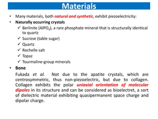
![Other natural materials
Biological materials exhibiting piezoelectric properties include:
Tendon
Silk
Wood due to piezoelectric texture
Enamel
Dentin
DNA
Synthetic crystals
Gallium orthophosphate (GaPO4), a quartz analogic crystal
Langasite (La3Ga5SiO14), a quartz analogic crystal
Synthetic
ceramics
Barium titanate (BaTiO3)
Lead titanate (PbTiO3)
Lead zirconate titanate (Pb[ZrxTi1−x]O3 0≤x≤1)
Polymers
Polyvinylidene fluoride (PVDF)](https://image.slidesharecdn.com/piezoelectricity-130726144833-phpapp02/85/Piezoelectricity-Think-Locally-Act-Globally-14-320.jpg)
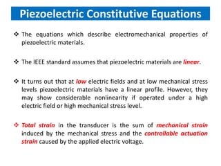
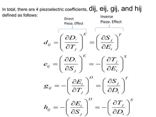
![• These may be combined into so called coupled equations, of which the
strain-charge form is:
Where [d] is the matrix for the direct piezoelectric effect and [dt] is the matrix for the
converse piezoelectric effect. The superscript E indicates a zero, or constant, electric field; the
superscript T indicates a zero, or constant, stress field; and the superscript t stands for
transposition of a matrix.
t T
E
S s T d E
D d T E
where the indexes i, j = 1, 2, . . . ,6
and m, k = 1, 2, 3 refer to different
directions within the material
coordinate system.](https://image.slidesharecdn.com/piezoelectricity-130726144833-phpapp02/85/Piezoelectricity-Think-Locally-Act-Globally-22-320.jpg)


Piezoelectricity involves using crystals that generate an electric charge in response to applied mechanical stress. Some materials that exhibit piezoelectricity include quartz, bone, wood, and synthetic ceramics. The document discusses the piezoelectric effect and electromechanical effect at the crystal structure level. It also provides the mathematical descriptions and constitutive equations for relating mechanical and electrical behavior in piezoelectric materials. The main applications discussed are piezoelectric actuators and transducers used in microelectromechanical systems.


