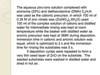
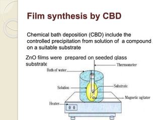
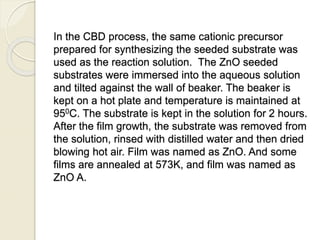
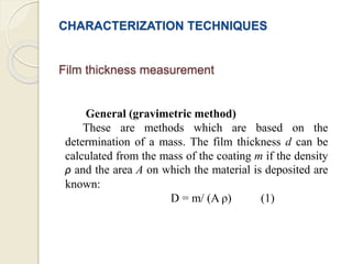
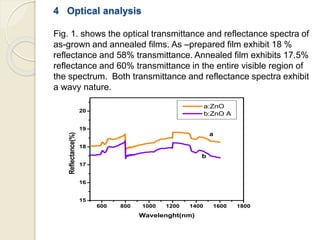
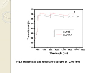
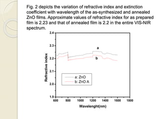
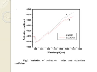
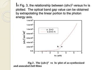
The document discusses the preparation and characterization of zinc oxide (ZnO) thin films using two-step chemical methods, focusing on their applications in gas sensors and electronic displays. The films were synthesized using Chemical Bath Deposition (CBD) on seeded substrates with structural, optical, and electrical properties analyzed through various techniques. Results indicate that the films exhibit n-type conductivity, high crystallinity, and suitable optical characteristics, including a reflectance of 18% and transmittance of 58% for as-prepared films.


![Thin_Film_Technology_introduction[1]](https://cdn.slidesharecdn.com/ss_thumbnails/1b4496c8-2102-411b-8465-a3dd3f398327-150205034538-conversion-gate02-thumbnail.jpg?width=640&height=640&fit=bounds)


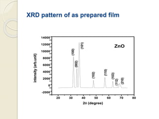
![Polymer [ बहुलक ] Chemistry Notes PDF - Irfanullah Mehar - JJ Sir Chemistry.pdf](https://cdn.slidesharecdn.com/ss_thumbnails/polymerchemistrynotespdf-irfanullahmehar-jjsirchemistry-260210172118-3f9b37f7-thumbnail.jpg?width=640&height=640&fit=bounds)


