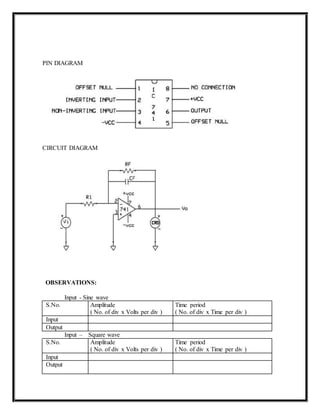
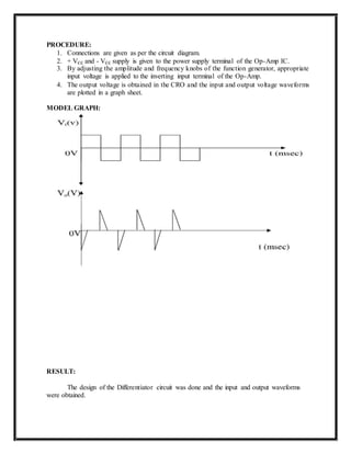
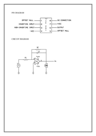
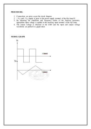
LIC EXPERIMENTS
EX.NO. DIFFERENTIATOR
AIM:
To design a Differentiator circuit for the given specifications using Op-Amp IC 741.
APPARATUS REQUIRED:
S.No Name of the Apparatus Range Quantity
1. Function Generator 3 MHz 1
2. CRO 30 MHz 1
3. Dual RPS 0 – 30 V 1
4. Op-Amp IC 741 1
5. Bread Board 1
6. Resistors
7. Capacitors
8. Connecting wires and probes As required
THEORY:
The differentiator circuit performs the mathematical operation of differentiation; that
is, the output waveform is the derivative of the input waveform. The differentiator may be
constructed from a basic inverting amplifier if an input resistor R1 is replaced by a capacitor
C1. The expression for the output voltage is given as, Vo = - Rf C1 (dVi /dt)
Here the negative sign indicates that the output voltage is 180 0 out of phase with the
input signal. A resistor Rcomp = Rf is normally connected to the non-inverting input terminal of
the op-amp to compensate for the input bias current. A workable differentiator can be
designed by implementing the following steps:
1. Select fa equal to the highest frequency of the input signal to be differentiated. Then,
assuming a value of C1 < 1 µF, calculate the value of R f.
2. Choose fb = 20 fa and calculate the values of R1 and Cf so that R1C1 = Rf Cf.
3. The differentiator is most commonly used in waveshaping circuits to detect high
frequency components in an input signal and also as a rate–of–change detector in FM
modulators.
DESIGN:
Given fa = ---------------
We know the frequency at which the gain is 0 dB, fa = 1 / (2π Rf C1)
Let us assume C1 = 0.1 µF; then
Rf = _________
Since fb = 20 fa, fb = ---------------
We know that the gain limiting frequency fb = 1 / (2π R1 C1)
Hence R1 = _________
Also since R1C1 = Rf Cf ;
Cf = _________
PIN DIAGRAM
CIRCUIT DIAGRAM
OBSERVATIONS:
Input - Sine wave
S.No. Amplitude Time period
( No. of div x Volts per div ) ( No. of div x Time per div )
Input
Output
Input – Square wave
S.No. Amplitude Time period
( No. of div x Volts per div ) ( No. of div x Time per div )
Input
Output
PROCEDURE:
1. Connections are given as per the circuit diagram.
2. + Vcc and - Vcc supply is given to the power supply terminal of the Op-Amp IC.
3. By adjusting the amplitude and frequency knobs of the function generator, appropriate
input voltage is applied to the inverting input terminal of the Op-Amp.
4. The output voltage is obtained in the CRO and the input and output voltage waveforms
are plotted in a graph sheet.
MODEL GRAPH:
RESULT:
The design of the Differentiator circuit was done and the input and output waveforms
were obtained.
INTEGRATOR
AIM:
To design an Integrator circuit for the given specifications using Op-Amp IC 741.
APPARATUS REQUIRED:
S.No Name of the Apparatus Range Quantity
1. Function Generator 3 MHz 1
2. CRO 30 MHz 1
3. Dual RPS 0 – 30 V 1
4. Op-Amp IC 741 1
5. Bread Board 1
6. Resistors
7. Capacitors
8. Connecting wires and probes As required
THEORY:
A circuit in which the output voltage waveform is the integral of the input voltage
waveform is the integrator. Such a circuit is obtained by using a basic inverting amplifier
configuration if the feedback resistor Rf is replaced by a capacitor Cf . The expression for
the output voltage is given as,
Vo = - (1/Rf C1) ∫ Vi dt
Here the negative sign indicates that the output voltage is 180 0 out of phase with the
input signal. Normally between fa and fb the circuit acts as an integrator. Generally, the
value of fa < fb . The input signal will be integrated properly if the Time period T of the
signal is larger than or equal to Rf Cf. That is,
T ≥ Rf Cf
The integrator is most commonly used in analog computers and ADC and signal-
wave shaping circuits.
DESIGN:
We know the frequency at which the gain is 0 dB,
fb = 1 / (2π R1 Cf)
Therefore fb = _____
Since fb = 10 fa, and also the gain limiting frequency
fa = 1 / (2π Rf Cf)
We get, Rf = _______ and
Hence R1 = __________
PIN DIAGRAM
CIRCUIT DIAGRAM
PROCEDURE:
1. Connections are given as per the circuit diagram.
2. + Vcc and - Vcc supply is given to the power supply terminal of the Op-Amp IC.
3. By adjusting the amplitude and frequency knobs of the function generator,
appropriate input voltage is applied to the inverting input terminal of the Op-Amp.
4. The output voltage is obtained in the CRO and the input and output voltage
waveforms are plotted in a graph sheet.
MODEL GRAPH
REVIEW QUESTIONS:
1. Why integrators are preferred over differentiators in analog computers?
Integrators are more linear than the differentiators and the integrators reduce the power
consumption than the high pass filter.
2. What are the applications of current sources?
Transistor current sources are widely used in analog ICs both as biasing elements and as
load devices for amplifier stages.
3. Justify the reasons for using current sources in integrated circuits.
*superior insensitivity of circuit performance to power supply variations and
temperature.
*more economical than resistors in terms of die area required to provide bias currents of
small value.
*When used as load element, the high incremental resistance of current source results in
high voltage gains at low supply voltages.
4. What is a differentiator?
A differentiator is the circuit which perform the mathematical operation of
differentiation, i.e., the output waveform is the derivative of the input waveform. The
output voltage is given by VO= -R fCi(d (Vi) / dt) Where Rf is the feedback resistor,
Ci is the input capacitance and Vi is the input voltage
5. What are the main drawbacks of ideal differentiator?
The main drawbacks of ideal differentiator are :
1. At high frequency, the differentiator may become unstable and break into
Oscillation.
2. The input impedance decreases with increase in frequency, thereby making the circuit
sensitive to high frequency noise.
RESULT:
The design of the Integrator circuit was done and the input and output waveforms
were obtained.

Ex 2 differentiator&integrator

  • 1.
  • 2.
    EX.NO. DIFFERENTIATOR AIM: To designa Differentiator circuit for the given specifications using Op-Amp IC 741. APPARATUS REQUIRED: S.No Name of the Apparatus Range Quantity 1. Function Generator 3 MHz 1 2. CRO 30 MHz 1 3. Dual RPS 0 – 30 V 1 4. Op-Amp IC 741 1 5. Bread Board 1 6. Resistors 7. Capacitors 8. Connecting wires and probes As required THEORY: The differentiator circuit performs the mathematical operation of differentiation; that is, the output waveform is the derivative of the input waveform. The differentiator may be constructed from a basic inverting amplifier if an input resistor R1 is replaced by a capacitor C1. The expression for the output voltage is given as, Vo = - Rf C1 (dVi /dt) Here the negative sign indicates that the output voltage is 180 0 out of phase with the input signal. A resistor Rcomp = Rf is normally connected to the non-inverting input terminal of the op-amp to compensate for the input bias current. A workable differentiator can be designed by implementing the following steps: 1. Select fa equal to the highest frequency of the input signal to be differentiated. Then, assuming a value of C1 < 1 µF, calculate the value of R f. 2. Choose fb = 20 fa and calculate the values of R1 and Cf so that R1C1 = Rf Cf. 3. The differentiator is most commonly used in waveshaping circuits to detect high frequency components in an input signal and also as a rate–of–change detector in FM modulators. DESIGN: Given fa = --------------- We know the frequency at which the gain is 0 dB, fa = 1 / (2π Rf C1) Let us assume C1 = 0.1 µF; then Rf = _________ Since fb = 20 fa, fb = --------------- We know that the gain limiting frequency fb = 1 / (2π R1 C1) Hence R1 = _________ Also since R1C1 = Rf Cf ; Cf = _________
  • 3.
    PIN DIAGRAM CIRCUIT DIAGRAM OBSERVATIONS: Input- Sine wave S.No. Amplitude Time period ( No. of div x Volts per div ) ( No. of div x Time per div ) Input Output Input – Square wave S.No. Amplitude Time period ( No. of div x Volts per div ) ( No. of div x Time per div ) Input Output
  • 4.
    PROCEDURE: 1. Connections aregiven as per the circuit diagram. 2. + Vcc and - Vcc supply is given to the power supply terminal of the Op-Amp IC. 3. By adjusting the amplitude and frequency knobs of the function generator, appropriate input voltage is applied to the inverting input terminal of the Op-Amp. 4. The output voltage is obtained in the CRO and the input and output voltage waveforms are plotted in a graph sheet. MODEL GRAPH: RESULT: The design of the Differentiator circuit was done and the input and output waveforms were obtained.
  • 5.
    INTEGRATOR AIM: To design anIntegrator circuit for the given specifications using Op-Amp IC 741. APPARATUS REQUIRED: S.No Name of the Apparatus Range Quantity 1. Function Generator 3 MHz 1 2. CRO 30 MHz 1 3. Dual RPS 0 – 30 V 1 4. Op-Amp IC 741 1 5. Bread Board 1 6. Resistors 7. Capacitors 8. Connecting wires and probes As required THEORY: A circuit in which the output voltage waveform is the integral of the input voltage waveform is the integrator. Such a circuit is obtained by using a basic inverting amplifier configuration if the feedback resistor Rf is replaced by a capacitor Cf . The expression for the output voltage is given as, Vo = - (1/Rf C1) ∫ Vi dt Here the negative sign indicates that the output voltage is 180 0 out of phase with the input signal. Normally between fa and fb the circuit acts as an integrator. Generally, the value of fa < fb . The input signal will be integrated properly if the Time period T of the signal is larger than or equal to Rf Cf. That is, T ≥ Rf Cf The integrator is most commonly used in analog computers and ADC and signal- wave shaping circuits. DESIGN: We know the frequency at which the gain is 0 dB, fb = 1 / (2π R1 Cf) Therefore fb = _____ Since fb = 10 fa, and also the gain limiting frequency fa = 1 / (2π Rf Cf) We get, Rf = _______ and Hence R1 = __________
  • 6.
  • 7.
    PROCEDURE: 1. Connections aregiven as per the circuit diagram. 2. + Vcc and - Vcc supply is given to the power supply terminal of the Op-Amp IC. 3. By adjusting the amplitude and frequency knobs of the function generator, appropriate input voltage is applied to the inverting input terminal of the Op-Amp. 4. The output voltage is obtained in the CRO and the input and output voltage waveforms are plotted in a graph sheet. MODEL GRAPH
  • 8.
    REVIEW QUESTIONS: 1. Whyintegrators are preferred over differentiators in analog computers? Integrators are more linear than the differentiators and the integrators reduce the power consumption than the high pass filter. 2. What are the applications of current sources? Transistor current sources are widely used in analog ICs both as biasing elements and as load devices for amplifier stages. 3. Justify the reasons for using current sources in integrated circuits. *superior insensitivity of circuit performance to power supply variations and temperature. *more economical than resistors in terms of die area required to provide bias currents of small value. *When used as load element, the high incremental resistance of current source results in high voltage gains at low supply voltages. 4. What is a differentiator? A differentiator is the circuit which perform the mathematical operation of differentiation, i.e., the output waveform is the derivative of the input waveform. The output voltage is given by VO= -R fCi(d (Vi) / dt) Where Rf is the feedback resistor, Ci is the input capacitance and Vi is the input voltage 5. What are the main drawbacks of ideal differentiator? The main drawbacks of ideal differentiator are : 1. At high frequency, the differentiator may become unstable and break into Oscillation. 2. The input impedance decreases with increase in frequency, thereby making the circuit sensitive to high frequency noise. RESULT: The design of the Integrator circuit was done and the input and output waveforms were obtained.