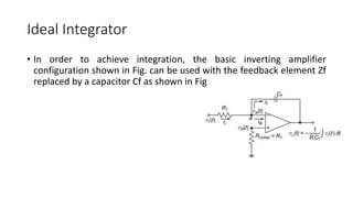
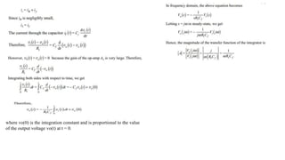
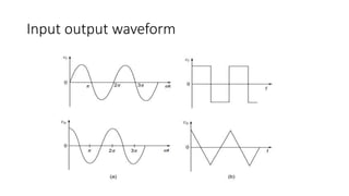
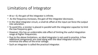
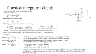
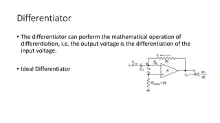
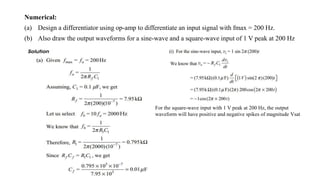
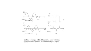
Integrator
&
Differentiator
Integrator
• A circuit in which the output voltage waveform is the time integral of
the input voltage waveform is called integrator or integrating
amplifier
Ideal Integrator
• In order to achieve integration, the basic inverting amplifier
configuration shown in Fig. can be used with the feedback element Zf
replaced by a capacitor Cf as shown in Fig
where vo(0) is the integration constant and is proportional to the value
of the output voltage vo(t) at t = 0.
Input output waveform
Limitations of Integrator
• At w = 0, the gain of the integrator is infinite.
• As the frequency increases, the gain of the integrator decreases.
• In the ideal integrator circuit, a small dc offset at the input can force the output
into saturation.
• To avoid this, a resistor is placed in parallel with the integrator capacitor to limit
the low frequency gain.
• However, this has an undesirable side effect of limiting the useful integration
range at higher frequencies.
• Due to the above limitations, an ideal integrator is not used in practice. A few
additional components are used along with the ideal integrator circuit to
minimise the effect of the error voltage.
• Such an integrator is called the practical integrator.
Practical Integrator Circuit
The frequency responses of the ideal integrator and the lossy integrator are shown
in Fig. The ideal integrator of Fig. exhibits a –6 dB/octave (–20 dB/decade) slope
through the useful integration range. The frequency fb is the frequency at which
the transfer function or gain of the integrator is 1 or 0 dB
Differentiator
• The differentiator can perform the mathematical operation of
differentiation, i.e. the output voltage is the differentiation of the
input voltage.
• Ideal Differentiator
Limitations of Ideal Differentiator
• When compared to integrator circuits, the differentiator circuits are more
susceptible to noise. The input noise fluctuations of small amplitudes will
have large derivatives. When differentiated, these noise fluctuations will
generate large noise signals at the output, which will introduce a poor
signal-to-noise-ratio. This problem may be minimised by placing a resistor
in series with the input capacitor. This modified circuit differentiates only
low frequency signals with a constant high frequency gain.
• In a differentiator circuit, the limitations due to noise, stability and input
impedance can pose problems. In order to minimise noise and aid in
stability, a small capacitor may be placed in parallel with Rf , which will
reduce the high frequency gain. In order to place a lower limit on the input
impedance, a resistor may be connected in series with the differentiating
capacitor. The addition of either component will limit the upper range of
differentiation.
A practical differentiator circuit is shown in Fig. This eliminates the limitations of
noise and stability. The effective current at the node a is zero. The input current
practical differentiator
Applying Kirchhoff’s Current Law at node a,
Frequency response of practical differentiator
shows that the gain increases at +20 dB/decade for frequency
ranges of f < fb and decreases at the rate of –20 dB/decade for
f > fb. It is shown as the gain characteristics in Fig. in dotted
lines. This 40 dB/decade variation in gain is due to the R1C1
and RfCf factors. For the ideal differentiator of Fig., the
frequency response would have steadily increased at 20 dB /
decade even beyond fb, which could cause stability problems at
high frequencies. The gain for the practical differentiator circuit
is reduced significantly and this avoids the high frequency
noise, and results in better stability
The value fb is normally selected such that fa< fb <fc where fc
denotes the unity gain-bandwidth of the op-amp in open loop
configuration mode
Numerical:
(a) Design a differentiator using op-amp to differentiate an input signal with fmax = 200 Hz.
(b) Also draw the output waveforms for a sine-wave and a square-wave input of 1 V peak at 200 Hz
For the square-wave input with 1 V peak at 200 Hz, the output
waveform will have positive and negative spikes of magnitude Vsat
(a) Sine-wave input and its differentiated cosine output and
(b) Square wave input and its differentiated spike output
Instrumentation Amplifier

M_2_Integrator(Analog Electronics Integrator Using OP Amps).pptx

  • 1.
  • 2.
    Integrator • A circuitin which the output voltage waveform is the time integral of the input voltage waveform is called integrator or integrating amplifier
  • 3.
    Ideal Integrator • Inorder to achieve integration, the basic inverting amplifier configuration shown in Fig. can be used with the feedback element Zf replaced by a capacitor Cf as shown in Fig
  • 4.
    where vo(0) isthe integration constant and is proportional to the value of the output voltage vo(t) at t = 0.
  • 5.
  • 6.
    Limitations of Integrator •At w = 0, the gain of the integrator is infinite. • As the frequency increases, the gain of the integrator decreases. • In the ideal integrator circuit, a small dc offset at the input can force the output into saturation. • To avoid this, a resistor is placed in parallel with the integrator capacitor to limit the low frequency gain. • However, this has an undesirable side effect of limiting the useful integration range at higher frequencies. • Due to the above limitations, an ideal integrator is not used in practice. A few additional components are used along with the ideal integrator circuit to minimise the effect of the error voltage. • Such an integrator is called the practical integrator.
  • 7.
    Practical Integrator Circuit Thefrequency responses of the ideal integrator and the lossy integrator are shown in Fig. The ideal integrator of Fig. exhibits a –6 dB/octave (–20 dB/decade) slope through the useful integration range. The frequency fb is the frequency at which the transfer function or gain of the integrator is 1 or 0 dB
  • 8.
    Differentiator • The differentiatorcan perform the mathematical operation of differentiation, i.e. the output voltage is the differentiation of the input voltage. • Ideal Differentiator
  • 10.
    Limitations of IdealDifferentiator • When compared to integrator circuits, the differentiator circuits are more susceptible to noise. The input noise fluctuations of small amplitudes will have large derivatives. When differentiated, these noise fluctuations will generate large noise signals at the output, which will introduce a poor signal-to-noise-ratio. This problem may be minimised by placing a resistor in series with the input capacitor. This modified circuit differentiates only low frequency signals with a constant high frequency gain. • In a differentiator circuit, the limitations due to noise, stability and input impedance can pose problems. In order to minimise noise and aid in stability, a small capacitor may be placed in parallel with Rf , which will reduce the high frequency gain. In order to place a lower limit on the input impedance, a resistor may be connected in series with the differentiating capacitor. The addition of either component will limit the upper range of differentiation.
  • 11.
    A practical differentiatorcircuit is shown in Fig. This eliminates the limitations of noise and stability. The effective current at the node a is zero. The input current practical differentiator Applying Kirchhoff’s Current Law at node a,
  • 12.
    Frequency response ofpractical differentiator shows that the gain increases at +20 dB/decade for frequency ranges of f < fb and decreases at the rate of –20 dB/decade for f > fb. It is shown as the gain characteristics in Fig. in dotted lines. This 40 dB/decade variation in gain is due to the R1C1 and RfCf factors. For the ideal differentiator of Fig., the frequency response would have steadily increased at 20 dB / decade even beyond fb, which could cause stability problems at high frequencies. The gain for the practical differentiator circuit is reduced significantly and this avoids the high frequency noise, and results in better stability The value fb is normally selected such that fa< fb <fc where fc denotes the unity gain-bandwidth of the op-amp in open loop configuration mode
  • 13.
    Numerical: (a) Design adifferentiator using op-amp to differentiate an input signal with fmax = 200 Hz. (b) Also draw the output waveforms for a sine-wave and a square-wave input of 1 V peak at 200 Hz For the square-wave input with 1 V peak at 200 Hz, the output waveform will have positive and negative spikes of magnitude Vsat
  • 14.
    (a) Sine-wave inputand its differentiated cosine output and (b) Square wave input and its differentiated spike output
  • 15.

Editor's Notes

  • #11 As the frequency increases, the gain of the differentiator increases due to the reduction of input impedance X C1=1/2*pifc1 . Therefore, at high frequencies, the differentiator will become unstable due to very high gain and it may enter into saturation. This makes the circuit very sensitive to noise and the stability is affected. The noise component may override the signal also.