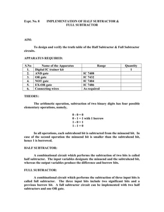
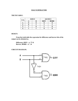
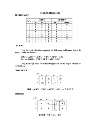
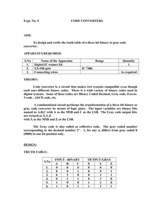
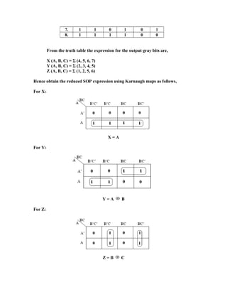
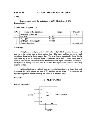
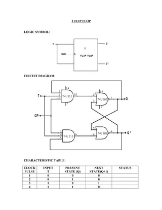
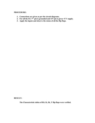
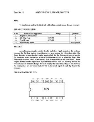
The document outlines a syllabus for a laboratory course on linear and digital integrated circuits, detailing various experiments and applications involving op-amps and timer ICs. It includes experiments on designing inverting and non-inverting amplifiers, differentiators and integrators, and multivibrators, while emphasizing procedures, theoretical concepts, and circuit designs. Each experiment aims to verify and analyze the functionalities of different electronic components using specific apparatus.

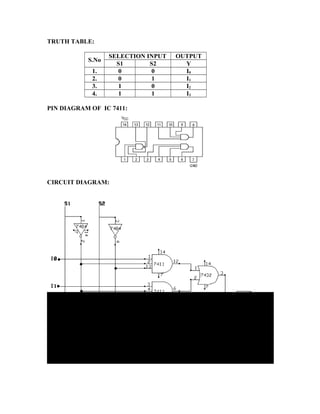
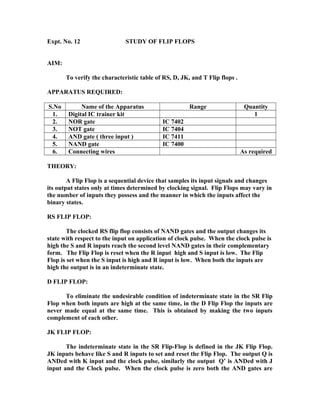
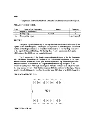
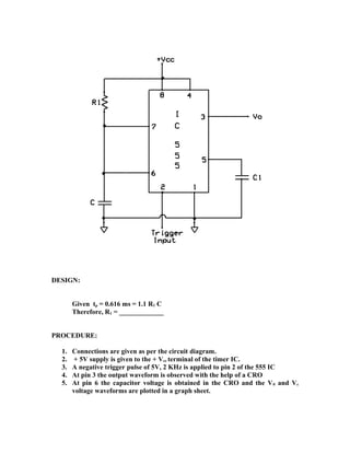
![AIM:
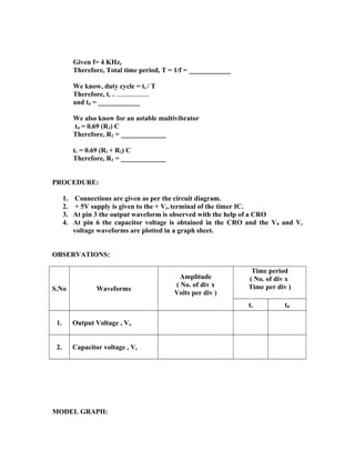
To design an astable multivibrator circuit for the given specifications using
555 Timer IC.
APPARATUS REQUIRED:
S. No Name of the Apparatus Range Quantity
1. Function Generator 3 MHz 1
2. CRO 30 MHz 1
3. Dual RPS 0 – 30 V 1
4. Timer IC IC 555 1
5. Bread Board 1
6. Resistors
7. Capacitors
8. Connecting wires and probes As required
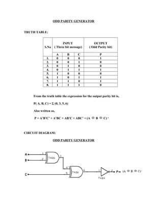
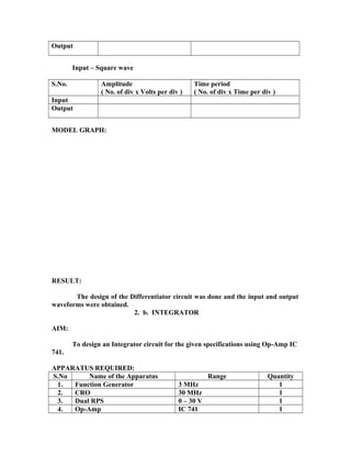
THEORY:
An astable multivibrator, often called a free-running multivibrator, is a
rectangular-wave-generating circuit. This circuit do not require an external trigger
to change the state of the output. The time during which the output is either high or
low is determined by two resistors and a capacitor, which are connected externally
to the 555 timer. The time during which the capacitor charges from 1/3 Vcc to 2/3 Vcc
is equal to the time the output is high and is given by,
tc = 0.69 (R1 + R2) C
Similarly the time during which the capacitor discharges from 2/3 Vcc to 1/3
Vcc is equal to the time the output is low and is given by,
td = 0.69 (R2) C
Thus the total time period of the output waveform is,
T = tc + td = 0.69 (R1 + 2 R2) C
The term duty cycle is often used in conjunction with the astable
multivibrator. The duty cycle is the ratio of the time tc during which the output is
high to the total time period T. It is generally expressed in percentage. In equation
form,
% duty cycle = [(R1 + R2) / (R1 + 2 R2)] x 100
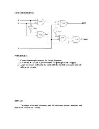
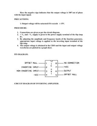
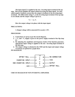
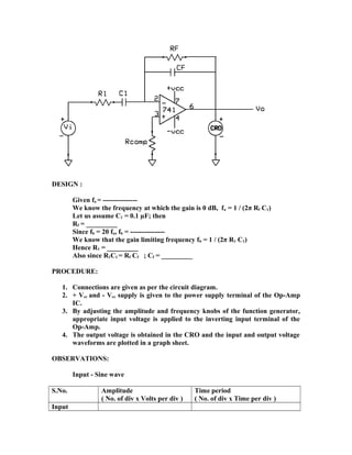
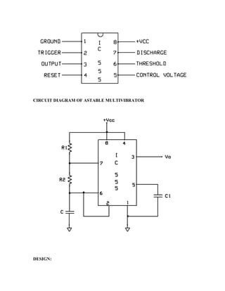
PIN DIAGRAM:](https://image.slidesharecdn.com/101495802-ee2258-lm-1-150908173218-lva1-app6891-180320142412/85/computer-architecture-notes-15-320.jpg)

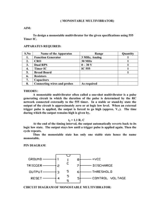
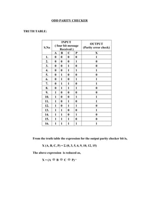
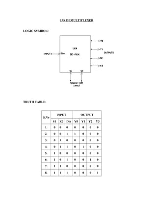
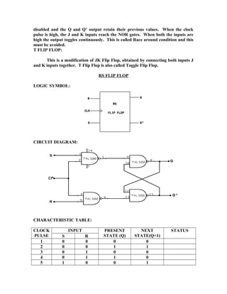
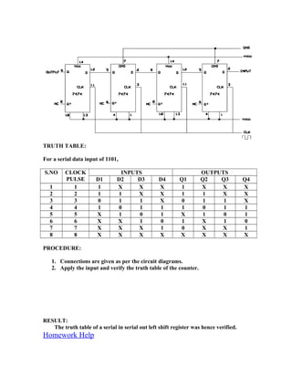
![AIM:
To design the logic circuit and verify the truth table of the given Boolean
expression,
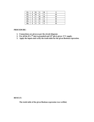
F (A, B, C, D) = Σ (0, 1, 2, 5, 8, 9, 10)
[Design can be changed by changing the Boolean expression]
APPARATUS REQUIRED:
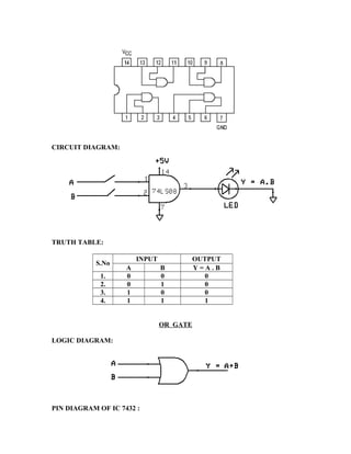
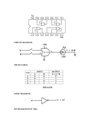
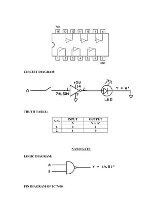
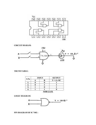
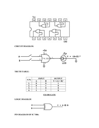
S.No Name of the Apparatus Range Quantity
1. Digital IC trainer kit 1
2. AND gate IC 7408
3. OR gate IC 7432
4. NOT gate IC 7404
5. NAND gate IC 7400
6. NOR gate IC 7402
7. EX-OR gate IC 7486
8. Connecting wires As required
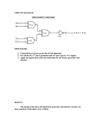
DESIGN:
Given , F (A,B,C,D) = Σ (0,1,2,5,8,9,10)
The output function F has four input variables hence a four variable
Karnaugh Map is used to obtain a simplified expression for the output as shown,
From the K-Map,
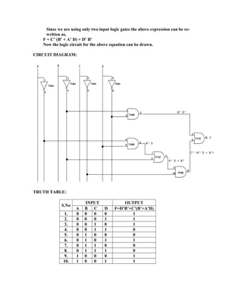
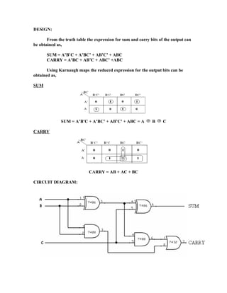
F = B’ C’ + D’ B’ + A’ C’ D](https://image.slidesharecdn.com/101495802-ee2258-lm-1-150908173218-lva1-app6891-180320142412/85/computer-architecture-notes-30-320.jpg)