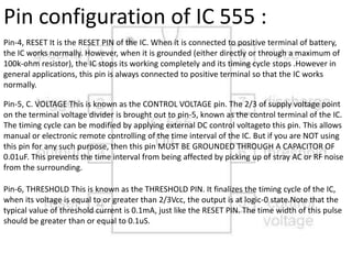
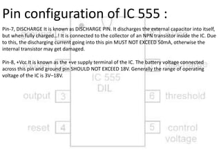
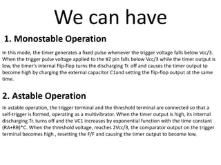
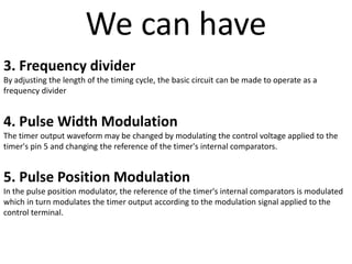
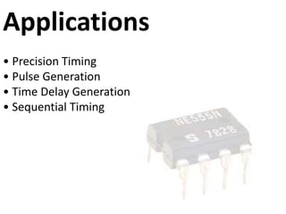
What Is A 555 Timer?
1 A 555 Timer is an 8 pin mini dual-in-line package
IC.
2 The 555 IC is capable of producing accurate time
delays and/ or oscillations.
3 Introduced in 1972 by SigNetics.(Signal Networks
Electronics)
4 The 555 is still in widespread use,thanks to its ease
of use, low price, and good stability.
25 Transistors
2 Diodes
15 Resistors
A standard 555 IC package consist of :
Imagination
Reality
Features
• High Current Drive Capability (200mA)
• Adjustable Duty Cycle
• Temperature Stability of 0.005%/°C
• Timing From μSec to Hours
• Turn off Time Less Than 2μSec
• Monostable and Astable operation
• Ability to operate from a wide range of supply
voltages
• Trigger and reset inputs are logic compatible
Internal Block Diagram
what is inside 555?A functional block diagram of 555 timer is given below. The device consists of two
comparators ,2 transistors, a flip-flop and buffered outputs stage. The reference
voltages for the two comparators inside the 555 are produced across a voltage
divider consisting of three equal resistors of 5K ohms each. Look at the given
block diagram of the IC, to see that there are three resistors of 5kohm each
connected in series. These three resistors produce 1/3 and 2/3 voltage levels for
controlling the action of trigger and threshold comparators inside the IC. Due to
this arrangement of the three resistors, the IC has a typical code
number as IC555.
The threshold comparator is referenced at 2/3 Vcc and the trigger comparator is
referenced at 1/3Vcc. The two comparators
control the flip-flop which, in turn, controls
the state of the output i.e. either ON or OFF
states.
Pin configuration of IC 555 :
Pin-1, GROUND: It is the GROUND PIN of the IC. The negative terminal of DC power supply or
battery is connected to this pin. Note that this pin should be connected directly to ground and
NOT through any resistor or capacitor. If done so, the IC will not function properly and may heat
up and get damaged. This happens because all the semiconductor blocks inside the IC will be
raised by certain amount of stray voltage and will damage the IC.IC 555
Pin-2, TRIGGER It is known as TRIGGER PIN. As the name suggests in triggers i.e. starts the
timing cycle of the IC. It is connected to the inverting input terminal of trigger comparator inside
the IC. It triggers when the voltage at this pin LESS THAN 1/3 of the supply voltage (Vcc). The
triggering circuit inside the IC is very sensitive and may be accidently activated due to
surrounding noise. To avoid this, the pin is always connected to a pull-up resistor (10k-ohm), if
this pin is used separately.
Pin-3, OUTPUT This is the OUTPUT PIN of the IC. It can SINK or SOURCE a maximum current of
200mA. Sinking the current means, when the output of the IC is at logic-0 state i.e. LOW and so
it can absorb current into its output. Similarly sourcing the current means, when the output of
the IC is at logic-1 i.e. HIGH and so it can give out current from its output.
Pin-4, RESET It is the RESET PIN of the IC. When it is connected to positive terminal of battery,
the IC works normally. However, when it is grounded (either directly or through a maximum of
100k-ohm resistor), the IC stops its working completely and its timing cycle stops .However in
general applications, this pin is always connected to positive terminal so that the IC works
normally.
Pin-5, C. VOLTAGE This is known as the CONTROL VOLTAGE pin. The 2/3 of supply voltage point
on the terminal voltage divider is brought out to pin-5, known as the control terminal of the IC.
The timing cycle can be modified by applying external DC control voltageto this pin. This allows
manual or electronic remote controlling of the time interval of the IC. But if you are NOT using
this pin for any such purpose, then this pin MUST BE GROUNDED THROUGH A CAPACITOR OF
0.01uF. This prevents the time interval from being affected by picking up of stray AC or RF noise
from the surrounding.
Pin-6, THRESHOLD This is known as the THRESHOLD PIN. It finalizes the timing cycle of the IC,
when its voltage is equal to or greater than 2/3Vcc, the output is at logic-0 state.Note that the
typical value of threshold current is 0.1mA, just like the RESET PIN. The time width of this pulse
should be greater than or equal to 0.1uS.
Pin configuration of IC 555 :
Pin-7, DISCHARGE It is known as DISCHARGE PIN. It discharges the external capacitor into itself,
but when fully charged…! It is connected to the collector of an NPN transistor inside the IC. Due
to this, the discharging current going into this pin MUST NOT EXCEED 50mA, otherwise the
internal transistor may get damaged.
Pin-8, +Vcc It is known as the +ve supply terminal of the IC. The battery voltage connected
across this pin and ground pin SHOULD NOT EXCEED 18V. Generally the range of operating
voltage of the IC is 3V–18V.
Pin configuration of IC 555 :
2. Astable Operation
We can have
1. Monostable Operation
In this mode, the timer generates a fixed pulse whenever the trigger voltage falls below Vcc/3.
When the trigger pulse voltage applied to the #2 pin falls below Vcc/3 while the timer output is
low, the timer's internal flip-flop turns the discharging Tr. off and causes the timer output to
become high by charging the external capacitor C1and setting the flip-flop output at the same
time.
In astable operation, the trigger terminal and the threshold terminal are connected so that a
self-trigger is formed, operating as a multivibrator. When the timer output is high, its internal
discharging Tr. turns off and the VC1 increases by exponential function with the time constant
(RA+RB)*C. When the threshold voltage, reaches 2Vcc/3, the comparator output on the trigger
terminal becomes high , resetting the F/F and causing the timer output to become low.
3. Frequency divider
By adjusting the length of the timing cycle, the basic circuit can be made to operate as a
frequency divider
4. Pulse Width Modulation
The timer output waveform may be changed by modulating the control voltage applied to the
timer's pin 5 and changing the reference of the timer's internal comparators.
We can have
5. Pulse Position Modulation
In the pulse position modulator, the reference of the timer's internal comparators is modulated
which in turn modulates the timer output according to the modulation signal applied to the
control terminal.
Applications
• Precision Timing
• Pulse Generation
• Time Delay Generation
• Sequential Timing

Timer 555

  • 1.
    What Is A555 Timer? 1 A 555 Timer is an 8 pin mini dual-in-line package IC. 2 The 555 IC is capable of producing accurate time delays and/ or oscillations. 3 Introduced in 1972 by SigNetics.(Signal Networks Electronics) 4 The 555 is still in widespread use,thanks to its ease of use, low price, and good stability.
  • 2.
    25 Transistors 2 Diodes 15Resistors A standard 555 IC package consist of :
  • 3.
  • 4.
  • 5.
    Features • High CurrentDrive Capability (200mA) • Adjustable Duty Cycle • Temperature Stability of 0.005%/°C • Timing From μSec to Hours • Turn off Time Less Than 2μSec • Monostable and Astable operation • Ability to operate from a wide range of supply voltages • Trigger and reset inputs are logic compatible
  • 6.
  • 7.
    what is inside555?A functional block diagram of 555 timer is given below. The device consists of two comparators ,2 transistors, a flip-flop and buffered outputs stage. The reference voltages for the two comparators inside the 555 are produced across a voltage divider consisting of three equal resistors of 5K ohms each. Look at the given block diagram of the IC, to see that there are three resistors of 5kohm each connected in series. These three resistors produce 1/3 and 2/3 voltage levels for controlling the action of trigger and threshold comparators inside the IC. Due to this arrangement of the three resistors, the IC has a typical code number as IC555. The threshold comparator is referenced at 2/3 Vcc and the trigger comparator is referenced at 1/3Vcc. The two comparators control the flip-flop which, in turn, controls the state of the output i.e. either ON or OFF states.
  • 8.
    Pin configuration ofIC 555 : Pin-1, GROUND: It is the GROUND PIN of the IC. The negative terminal of DC power supply or battery is connected to this pin. Note that this pin should be connected directly to ground and NOT through any resistor or capacitor. If done so, the IC will not function properly and may heat up and get damaged. This happens because all the semiconductor blocks inside the IC will be raised by certain amount of stray voltage and will damage the IC.IC 555 Pin-2, TRIGGER It is known as TRIGGER PIN. As the name suggests in triggers i.e. starts the timing cycle of the IC. It is connected to the inverting input terminal of trigger comparator inside the IC. It triggers when the voltage at this pin LESS THAN 1/3 of the supply voltage (Vcc). The triggering circuit inside the IC is very sensitive and may be accidently activated due to surrounding noise. To avoid this, the pin is always connected to a pull-up resistor (10k-ohm), if this pin is used separately. Pin-3, OUTPUT This is the OUTPUT PIN of the IC. It can SINK or SOURCE a maximum current of 200mA. Sinking the current means, when the output of the IC is at logic-0 state i.e. LOW and so it can absorb current into its output. Similarly sourcing the current means, when the output of the IC is at logic-1 i.e. HIGH and so it can give out current from its output.
  • 9.
    Pin-4, RESET Itis the RESET PIN of the IC. When it is connected to positive terminal of battery, the IC works normally. However, when it is grounded (either directly or through a maximum of 100k-ohm resistor), the IC stops its working completely and its timing cycle stops .However in general applications, this pin is always connected to positive terminal so that the IC works normally. Pin-5, C. VOLTAGE This is known as the CONTROL VOLTAGE pin. The 2/3 of supply voltage point on the terminal voltage divider is brought out to pin-5, known as the control terminal of the IC. The timing cycle can be modified by applying external DC control voltageto this pin. This allows manual or electronic remote controlling of the time interval of the IC. But if you are NOT using this pin for any such purpose, then this pin MUST BE GROUNDED THROUGH A CAPACITOR OF 0.01uF. This prevents the time interval from being affected by picking up of stray AC or RF noise from the surrounding. Pin-6, THRESHOLD This is known as the THRESHOLD PIN. It finalizes the timing cycle of the IC, when its voltage is equal to or greater than 2/3Vcc, the output is at logic-0 state.Note that the typical value of threshold current is 0.1mA, just like the RESET PIN. The time width of this pulse should be greater than or equal to 0.1uS. Pin configuration of IC 555 :
  • 10.
    Pin-7, DISCHARGE Itis known as DISCHARGE PIN. It discharges the external capacitor into itself, but when fully charged…! It is connected to the collector of an NPN transistor inside the IC. Due to this, the discharging current going into this pin MUST NOT EXCEED 50mA, otherwise the internal transistor may get damaged. Pin-8, +Vcc It is known as the +ve supply terminal of the IC. The battery voltage connected across this pin and ground pin SHOULD NOT EXCEED 18V. Generally the range of operating voltage of the IC is 3V–18V. Pin configuration of IC 555 :
  • 11.
    2. Astable Operation Wecan have 1. Monostable Operation In this mode, the timer generates a fixed pulse whenever the trigger voltage falls below Vcc/3. When the trigger pulse voltage applied to the #2 pin falls below Vcc/3 while the timer output is low, the timer's internal flip-flop turns the discharging Tr. off and causes the timer output to become high by charging the external capacitor C1and setting the flip-flop output at the same time. In astable operation, the trigger terminal and the threshold terminal are connected so that a self-trigger is formed, operating as a multivibrator. When the timer output is high, its internal discharging Tr. turns off and the VC1 increases by exponential function with the time constant (RA+RB)*C. When the threshold voltage, reaches 2Vcc/3, the comparator output on the trigger terminal becomes high , resetting the F/F and causing the timer output to become low.
  • 12.
    3. Frequency divider Byadjusting the length of the timing cycle, the basic circuit can be made to operate as a frequency divider 4. Pulse Width Modulation The timer output waveform may be changed by modulating the control voltage applied to the timer's pin 5 and changing the reference of the timer's internal comparators. We can have 5. Pulse Position Modulation In the pulse position modulator, the reference of the timer's internal comparators is modulated which in turn modulates the timer output according to the modulation signal applied to the control terminal.
  • 13.
    Applications • Precision Timing •Pulse Generation • Time Delay Generation • Sequential Timing