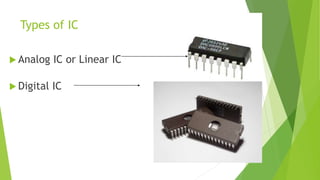
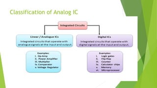
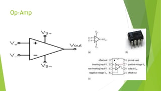
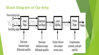
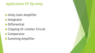
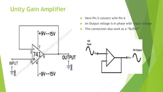
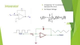
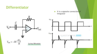
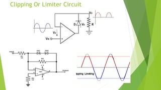
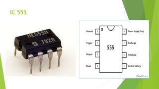
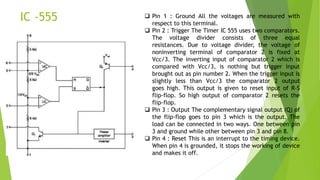
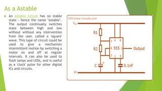
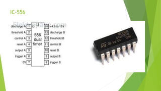
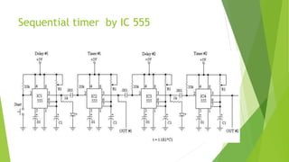
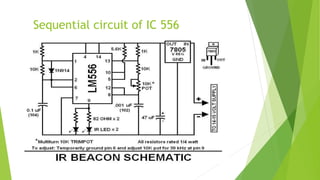
Integrated Circuit
Prepared by: D.H.Shukla
Need of IC
 An Integrated Circuits is defined as the circuit that comprises of elements
that are inseparable and interconnected electrically in such a way that the IC
cannot be separated for the reason of commerce and construction. Myriad
technologies can be used to build such a circuit. Today what we call an IC,
was originally known as a monolithic integrated circuit. It is believed that
Kilby created the first working IC back in 1958 and he won the Nobel Prize in
Physics in 2000 for his hard work. The first buyer for this invention was the US
Air Force.
 Through IC a sub branches are created like
 MSI
 LSI
 VSI
Types of IC
 Analog IC or Linear IC
 Digital IC
Advantages & Dis-Advantages
 Advantages :
1. The entire physical size of IC is extremely small than that of discrete circuit.
2. The weight of an IC is very less as compared entire discrete circuits.
3. It’s more reliable.
4. Because of their smaller size it has lower power consumption.
5. It can easily replace but it can hardly repair, in case of failure.
6. Because of an absence of parasitic and capacitance effect it has increased operating
speed.
7. Temperature differences between components of a circuit are small.
8. It has suitable for small signal operation.
9. The reduction in power consumption is achieved due to extremely small size of IC.
Continue…
 Disadvantages :-
1. Coils or indicators cannot be fabricated.
2. It can be handle only limited amount of power.
3. High grade P-N-P assembly is not possible.
4. It is difficult to be achieved low temperature coefficient.
5. The power dissipation is limited to 10 watts.
6. Low noise and high voltage operation are not easily obtained.
7. Inductors and transformers are needed connecting to exterior to the semiconductor chip as
it is not possible to fabricate inductor and transformers on the semiconductor chip surface.
8. Inductors cannot be fabricated directly.
Classification of Analog IC
Op-Amp
Block Diagram of Op-Amp
Parameters of Op-Amp
1. Input Offset Voltage
 Input offset voltage is the voltage that is applied between the two
input terminals of the op-amp to null the output
2. Input Offset Current
 Input Offset Current is the algebraic difference between the currents
into the inverting and non-inverting terminals.
3. Input Bias Current
 Input bias current is the average value of the inverting and non-
inverting current.
4. Common Mode Rejection Ratio (CMRR)
 CMRR is the ratio of the differential voltage gain to the common mode
voltage gain.
 CMRR = Differential Voltage Gain (Ad)/ Common Mode Voltage Gain
(Acm)
Continue..
5. Output Resistance
 Output Resistance is the equivalent resistance that is measured between the
output terminal (Pin 6) and Ground
6. Input Resistance
 Differential Input Resistance is the equivalent resistance that is measured
from any one of the input terminals by keeping the other terminal connected
to ground
7. Slew Rate (SR)
 Slew Rate is one of the most important parameters for selecting op-amps for
high frequencies. SR is the maximum rate of change of output voltage per
unit of time and is expressed in volts per microseconds.
8. Power Consumption
 For the 741 IC to operate properly, a certain amount of quiescent power must
be consumed by the op-amp. This power is called power consumption and
typical value is 85mW.
9. Gain Band Width Product
 When Output of Op-Amp is unity then bandwidth of Op-Amp is called Gain
Bandwidth Product
Characteristics of Op-Amp 741
 Infinite open-loop gain G = vout / vin
 Infinite input impedance Rin, and so zero input current
 Zero input offset voltage
 Infinite output voltage range
 Infinite bandwidth with zero phase shift and infinite slew rate
 Zero output impedance Rout
 Zero noise
 Infinite common-mode rejection ratio (CMRR)
 Infinite power supply rejection ratio.
Application Of Op-Amp
 Unity Gain Amplifier
 Integrator
 Differential
 Clipping Or Limiter Circuit
 Comparator
 Summing Amplifier
Unity Gain Amplifier
 Here Pin 2 connect with Pin 6
 An Output voltage is In phase with input voltage
 This connection also work as a “Buffer”
Integrator
 A Capacitor “C” is connected
between Pin 2 & 6
 An Output Voltage
Differentiator
 It is a opposite connection of
Integrator
Clipping Or Limiter Circuit
Comparator
Summing Point
IC 555
IC -555  Pin 1 : Ground All the voltages are measured with
respect to this terminal.
 Pin 2 : Trigger The Timer IC 555 uses two comparators.
The voltage divider consists of three equal
resistances. Due to voltage divider, the voltage of
noninverting terminal of comparator 2 is fixed at
Vcc/3. The inverting input of comparator 2 which is
compared with Vcc/3, is nothing but trigger input
brought out as pin number 2. When the trigger input is
slightly less than Vcc/3 the comparator 2 output
goes high. This output is given to reset input of R-S
flip-flop. So high output of comparator 2 resets the
flip-flop.
 Pin 3 : Output The complementary signal output (Q) of
the flip-flop goes to pin 3 which is the output. The
load can be connected in two ways. One between pin
3 and ground while other between pin 3 and pin 8.
 Pin 4 : Reset This is an interrupt to the timing device.
When pin 4 is grounded, it stops the working of device
and makes it off.
Continue….
 . Pin 5 : Control Voltage Input In most of the applications, external control voltage
input is not used. This pin is nothing but the inverting input terminal of comparator 1.
The voltage divider holds the voltage of this input at 2/3 Vcc. This is reference level
for comparator 1 with which threshold is compared. If reference level required is other
than 2/3 Vcc for comparator 1 then external input is to be given to pin 5. If external
input applied to pin 5 is alternating then the reference level for comparator 1 keeps on
changing above and below 2/3 Vcc. Due to this, the variable pulse width output is
possible:, This is called pulse width modulation, which is possible due to pin 5.
 Pin 6 : Threshold This is the noninverting input terminal of comparator 1. The external
voltage is applied to this pin 6. When this voltage is more than 2/3 Vcc, the comparator
1 output goes high. This is given to the set input of R-S flip-flop. Thus high output of
comparator 1 sets the flip-flop. This makes Q of flip-flop high and (7) low. Thus the
output of Timer IC 555 at pin 3 goes low. Remember that output at pin 3 is Q which is
complementary output of flip-flop. In short,
 Pin 7 : Discharge This pin is connected to the collector of the discharge transistor Qd.
When the output is high then Q is low and transistor Qd is off. It acts as an open circuit
to the external capacitor C to be connected across it, so capacitor C can charge as
described earlier. When output is low, Q is high which drives the base of Qd high,
driving transistor Qd in saturation. It acts as short circuit, shorting the external
capacitor C to be connected across it.
 Pin 8 : Supply +Vcc The IC 555 timer can work with any supply voltage between 4.5 V
and 16 V.
IC -555 as a Bi-stable
 A Bi-stable Mode or what is sometimes called
a Schmitt Trigger, has two stable states, high and
low. Taking the Trigger input low makes the
output of the circuit go into the high state. Taking
the Reset input low makes the output of the
circuit go into the low state. This type of circuit
is ideal for use in an automated model railway
system where the train is required to run back
and forth over the same piece of track. A push
button (or reed switch with a magnet on the
underside of the train) would be placed at each
end of the track so that when one is hit by the
train, it will either trigger or reset the bi-stable.
 The output of the 555 would control a DPDT relay
which would be wired as a reversing switch to
reverse the direction of current to the track,
thereby reversing the direction of the train.
AS a Mono-Stable
 A Monostable Circuit produces one pulse
of a set length in response to a trigger
input such as a push button. The output
of the circuit stays in the low state until
there is a trigger input, hence the name
"monostable" meaning "one stable
state". his type of circuit is ideal for use
in a "push to operate" system for a
model displayed at exhibitions. A visitor
can push a button to start a model's
mechanism moving, and the mechanism
will automatically switch off after a set
time
Choosing Timing Components for RC circuit in Timer
 Choosing capacitors with large capacitances will be a problem. This is because
electrolyte capacitors with large capacitances often tend to have wider
tolerance limits. So the actual values and the marked values may have a
significant difference.
 Large capacitance electrolyte capacitors will have high leakage currents
which can affect the timing accuracy as the capacitor charges. When choosing
capacitors with large capacitance and low leakage current, Tantalum
capacitors are a better option.
 It is better to avoid electrolyte capacitors that have a high working voltage
rating as they do not work efficiently when operated at a voltage 10% less
than their rated voltage.
 Hence, capacitors with working voltage greater than the VCC of the 555 timer
should be chosen
 When operating the 555 timer as an Astable multivibrator , the value of the
timing resistor should be at least 1 Kilo Ohms. If the idea is to build a low
power consumption circuit, then it is better to have higher values for the
timing resistors.
As a Astable
 An Astable Circuit has no stable
state - hence the name "astable".
The output continually switches
state between high and low
without without any intervention
from the user, called a 'square'
wave. This type of circuit could be
used to give a mechanism
intermittent motion by switching a
motor on and off at regular
intervals. It can also be used to
flash lamps and LEDs, and is useful
as a 'clock' pulse for other digital
ICs and circuits.
IC-556
Sequential timer by IC 555
Sequential circuit of IC 556
Thank you

Integrated circuit

  • 1.
  • 2.
    Need of IC An Integrated Circuits is defined as the circuit that comprises of elements that are inseparable and interconnected electrically in such a way that the IC cannot be separated for the reason of commerce and construction. Myriad technologies can be used to build such a circuit. Today what we call an IC, was originally known as a monolithic integrated circuit. It is believed that Kilby created the first working IC back in 1958 and he won the Nobel Prize in Physics in 2000 for his hard work. The first buyer for this invention was the US Air Force.  Through IC a sub branches are created like  MSI  LSI  VSI
  • 3.
    Types of IC Analog IC or Linear IC  Digital IC
  • 4.
    Advantages & Dis-Advantages Advantages : 1. The entire physical size of IC is extremely small than that of discrete circuit. 2. The weight of an IC is very less as compared entire discrete circuits. 3. It’s more reliable. 4. Because of their smaller size it has lower power consumption. 5. It can easily replace but it can hardly repair, in case of failure. 6. Because of an absence of parasitic and capacitance effect it has increased operating speed. 7. Temperature differences between components of a circuit are small. 8. It has suitable for small signal operation. 9. The reduction in power consumption is achieved due to extremely small size of IC.
  • 5.
    Continue…  Disadvantages :- 1.Coils or indicators cannot be fabricated. 2. It can be handle only limited amount of power. 3. High grade P-N-P assembly is not possible. 4. It is difficult to be achieved low temperature coefficient. 5. The power dissipation is limited to 10 watts. 6. Low noise and high voltage operation are not easily obtained. 7. Inductors and transformers are needed connecting to exterior to the semiconductor chip as it is not possible to fabricate inductor and transformers on the semiconductor chip surface. 8. Inductors cannot be fabricated directly.
  • 6.
  • 7.
  • 8.
  • 9.
    Parameters of Op-Amp 1.Input Offset Voltage  Input offset voltage is the voltage that is applied between the two input terminals of the op-amp to null the output 2. Input Offset Current  Input Offset Current is the algebraic difference between the currents into the inverting and non-inverting terminals. 3. Input Bias Current  Input bias current is the average value of the inverting and non- inverting current. 4. Common Mode Rejection Ratio (CMRR)  CMRR is the ratio of the differential voltage gain to the common mode voltage gain.  CMRR = Differential Voltage Gain (Ad)/ Common Mode Voltage Gain (Acm)
  • 10.
    Continue.. 5. Output Resistance Output Resistance is the equivalent resistance that is measured between the output terminal (Pin 6) and Ground 6. Input Resistance  Differential Input Resistance is the equivalent resistance that is measured from any one of the input terminals by keeping the other terminal connected to ground 7. Slew Rate (SR)  Slew Rate is one of the most important parameters for selecting op-amps for high frequencies. SR is the maximum rate of change of output voltage per unit of time and is expressed in volts per microseconds. 8. Power Consumption  For the 741 IC to operate properly, a certain amount of quiescent power must be consumed by the op-amp. This power is called power consumption and typical value is 85mW. 9. Gain Band Width Product  When Output of Op-Amp is unity then bandwidth of Op-Amp is called Gain Bandwidth Product
  • 11.
    Characteristics of Op-Amp741  Infinite open-loop gain G = vout / vin  Infinite input impedance Rin, and so zero input current  Zero input offset voltage  Infinite output voltage range  Infinite bandwidth with zero phase shift and infinite slew rate  Zero output impedance Rout  Zero noise  Infinite common-mode rejection ratio (CMRR)  Infinite power supply rejection ratio.
  • 12.
    Application Of Op-Amp Unity Gain Amplifier  Integrator  Differential  Clipping Or Limiter Circuit  Comparator  Summing Amplifier
  • 13.
    Unity Gain Amplifier Here Pin 2 connect with Pin 6  An Output voltage is In phase with input voltage  This connection also work as a “Buffer”
  • 14.
    Integrator  A Capacitor“C” is connected between Pin 2 & 6  An Output Voltage
  • 15.
    Differentiator  It isa opposite connection of Integrator
  • 16.
  • 17.
  • 18.
  • 19.
  • 20.
    IC -555 Pin 1 : Ground All the voltages are measured with respect to this terminal.  Pin 2 : Trigger The Timer IC 555 uses two comparators. The voltage divider consists of three equal resistances. Due to voltage divider, the voltage of noninverting terminal of comparator 2 is fixed at Vcc/3. The inverting input of comparator 2 which is compared with Vcc/3, is nothing but trigger input brought out as pin number 2. When the trigger input is slightly less than Vcc/3 the comparator 2 output goes high. This output is given to reset input of R-S flip-flop. So high output of comparator 2 resets the flip-flop.  Pin 3 : Output The complementary signal output (Q) of the flip-flop goes to pin 3 which is the output. The load can be connected in two ways. One between pin 3 and ground while other between pin 3 and pin 8.  Pin 4 : Reset This is an interrupt to the timing device. When pin 4 is grounded, it stops the working of device and makes it off.
  • 21.
    Continue….  . Pin5 : Control Voltage Input In most of the applications, external control voltage input is not used. This pin is nothing but the inverting input terminal of comparator 1. The voltage divider holds the voltage of this input at 2/3 Vcc. This is reference level for comparator 1 with which threshold is compared. If reference level required is other than 2/3 Vcc for comparator 1 then external input is to be given to pin 5. If external input applied to pin 5 is alternating then the reference level for comparator 1 keeps on changing above and below 2/3 Vcc. Due to this, the variable pulse width output is possible:, This is called pulse width modulation, which is possible due to pin 5.  Pin 6 : Threshold This is the noninverting input terminal of comparator 1. The external voltage is applied to this pin 6. When this voltage is more than 2/3 Vcc, the comparator 1 output goes high. This is given to the set input of R-S flip-flop. Thus high output of comparator 1 sets the flip-flop. This makes Q of flip-flop high and (7) low. Thus the output of Timer IC 555 at pin 3 goes low. Remember that output at pin 3 is Q which is complementary output of flip-flop. In short,  Pin 7 : Discharge This pin is connected to the collector of the discharge transistor Qd. When the output is high then Q is low and transistor Qd is off. It acts as an open circuit to the external capacitor C to be connected across it, so capacitor C can charge as described earlier. When output is low, Q is high which drives the base of Qd high, driving transistor Qd in saturation. It acts as short circuit, shorting the external capacitor C to be connected across it.  Pin 8 : Supply +Vcc The IC 555 timer can work with any supply voltage between 4.5 V and 16 V.
  • 22.
    IC -555 asa Bi-stable  A Bi-stable Mode or what is sometimes called a Schmitt Trigger, has two stable states, high and low. Taking the Trigger input low makes the output of the circuit go into the high state. Taking the Reset input low makes the output of the circuit go into the low state. This type of circuit is ideal for use in an automated model railway system where the train is required to run back and forth over the same piece of track. A push button (or reed switch with a magnet on the underside of the train) would be placed at each end of the track so that when one is hit by the train, it will either trigger or reset the bi-stable.  The output of the 555 would control a DPDT relay which would be wired as a reversing switch to reverse the direction of current to the track, thereby reversing the direction of the train.
  • 23.
    AS a Mono-Stable A Monostable Circuit produces one pulse of a set length in response to a trigger input such as a push button. The output of the circuit stays in the low state until there is a trigger input, hence the name "monostable" meaning "one stable state". his type of circuit is ideal for use in a "push to operate" system for a model displayed at exhibitions. A visitor can push a button to start a model's mechanism moving, and the mechanism will automatically switch off after a set time
  • 24.
    Choosing Timing Componentsfor RC circuit in Timer  Choosing capacitors with large capacitances will be a problem. This is because electrolyte capacitors with large capacitances often tend to have wider tolerance limits. So the actual values and the marked values may have a significant difference.  Large capacitance electrolyte capacitors will have high leakage currents which can affect the timing accuracy as the capacitor charges. When choosing capacitors with large capacitance and low leakage current, Tantalum capacitors are a better option.  It is better to avoid electrolyte capacitors that have a high working voltage rating as they do not work efficiently when operated at a voltage 10% less than their rated voltage.  Hence, capacitors with working voltage greater than the VCC of the 555 timer should be chosen  When operating the 555 timer as an Astable multivibrator , the value of the timing resistor should be at least 1 Kilo Ohms. If the idea is to build a low power consumption circuit, then it is better to have higher values for the timing resistors.
  • 25.
    As a Astable An Astable Circuit has no stable state - hence the name "astable". The output continually switches state between high and low without without any intervention from the user, called a 'square' wave. This type of circuit could be used to give a mechanism intermittent motion by switching a motor on and off at regular intervals. It can also be used to flash lamps and LEDs, and is useful as a 'clock' pulse for other digital ICs and circuits.
  • 26.
  • 27.
  • 28.
  • 29.