Unit-III Waveform Generator
•
1 like•1,057 views

Oscillators, Sine Wave, Square Wave, Triangular Wave, Saw Tooth Wave Generation, Schmitt Trigger, Window Detector

Recommended
More Related Content
What's hot
What's hot (20)
Similar to Unit-III Waveform Generator
Similar to Unit-III Waveform Generator (20)
More from Dr.Raja R
More from Dr.Raja R (20)
Recently uploaded
Recently uploaded (20)
Unit-III Waveform Generator
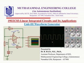
- 1. Presented by Dr. R. RAJA, M.E., Ph.D., Assistant Professor, Department of EEE, Muthayammal Engineering College, (Autonomous) Namakkal (Dt), Rasipuram – 637408 19EEC03-Linear Integrated Circuits and Its Applications Unit-III Waveform Generator MUTHAYAMMAL ENGINEERING COLLEGE (An Autonomous Institution) (Approved by AICTE, New Delhi, Accredited by NAAC, NBA & Affiliated to Anna University), Rasipuram - 637 408, Namakkal Dist., Tamil Nadu.
- 2. Unit-III Waveform Generator 8/28/2020 2 Oscillators, Sine Wave, Square Wave, Triangular Wave, Saw Tooth Wave Generation, Schmitt Trigger, Window Detector.
- 3. Oscillator What is an Oscillator? An oscillator is a circuit which produces a continuous, repeated, alternating waveform without any input. Oscillators basically convert unidirectional current flow from a DC source into an alternating waveform which is of the desired frequency, as decided by its circuit components. The basic principle behind the working of oscillators can be understood by analyzing the behavior of an LC tank circuit shown in Figure 1 below, which employs an inductor L and a completely pre-charged capacitor C as its components. Here, at first, the capacitor starts to discharge via the inductor, which results in the conversion of its electrical energy into the electromagnetic field, which can be stored in the inductor. Once the capacitor discharges completely, there will be no current flow in the circuit. 8/28/2020 3
- 4. Contd.. 8/28/2020 4 However, by then, the stored electromagnetic field would have generated a back- emf which results in the flow of current through the circuit in the same direction as that of before. This current flow through the circuit continues until the electromagnetic field collapses which result in the back-conversion of electromagnetic energy into electrical form, causing the cycle to repeat. However, now the capacitor would have charged with the opposite polarity, due to which one gets an oscillating waveform as the output.
- 5. Contd.. However, the oscillations which arise due to the inter-conversion between the two energy-forms cannot continue forever as they would be subjected to the effect of energy loss due to the resistance of the circuit. As a result, the amplitude of these oscillations decreases steadily to become zero, which makes them damped in nature. This indicates that in order to obtain the oscillations which are continuous and of constant amplitude, one needs to compensate for the energy loss. Nevertheless, it is to be noted that the energy supplied should be precisely controlled and must be equal to that of the energy lost in order to obtain the oscillations with constant amplitude. 8/28/2020 5
- 6. Contd.. This is because, if the energy supplied is more than the energy lost, then the amplitude of the oscillations will increase (Figure 2a) leading to a distorted output; while if the energy supplied is less than the energy lost, then the amplitude of the oscillations will decrease (Figure 2b) leading to unsustainable oscillations. 8/28/2020 6
- 7. Contd.. Practically, the oscillators are nothing but the amplifier circuits which are provided with a positive or regenerative feedback wherein a part of the output signal is fed back to the input (Figure 3). Here the amplifier consists of an amplifying active element which can be a transistor or an Op-Amp and the back-fed in-phase signal is held responsible to keep-up (sustain) the oscillations by making-up for the losses in the circuit. 8/28/2020 7
- 8. Contd.. 8/28/2020 8 Once the power supply is switched ON, the oscillations will be initiated in the system due to the electronic noise present in it. This noise signal travels around the loop, gets amplified and converges to a single frequency sine wave very quickly. The expression for the closed-loop gain of the oscillator shown in Figure 3 is given as: Where A is the voltage gain of the amplifier and β is the gain of the feedback network. Here, if Aβ > 1, then the oscillations will increase in amplitude (Figure 2a); while if Aβ < 1, then the oscillations will be damped (Figure 2b).
- 9. Contd.. On the other hand, Aβ = 1 leads to the oscillations which are of constant amplitude (Figure 2c). In other words, this indicates that if the feedback loop gain is small, then the oscillation dies-out, while if the gain of the feedback loop is large, then the output will be distorted; and only if the gain of feedback is unity, then the oscillations will be of constant amplitude leading to self-sustained oscillatory circuit. 8/28/2020 9
- 10. Contd.. Type of Oscillator There are many types of oscillators, but can broadly be classified into two main categories – Harmonic Oscillators (also known as Linear Oscillators) and Relaxation Oscillators. In a harmonic oscillator, the energy flow is always from the active components to the passive components and the frequency of oscillations is decided by the feedback path. Whereas in a relaxation oscillator, the energy is exchanged between the active and the passive components and the frequency of oscillations is determined by the charging and discharging time-constants involved in the process. Further, harmonic oscillators produce low-distorted sine-wave outputs while the relaxation oscillators generate non-sinusoidal (saw-tooth, triangular or square) wave-forms. 8/28/2020 10
- 11. Contd.. The main types of Oscillators include: Wien Bridge Oscillator RC Phase Shift Oscillator Hartley Oscillator Voltage Controlled Oscillator Colpitts Oscillator Clapp Oscillators Crystal Oscillators Armstrong Oscillator Tuned Collector Oscillator Gunn Oscillator Cross-Coupled Oscillators Ring Oscillators 8/28/2020 11
- 12. Contd.. Oscillators can be also be classified into various types depending on the parameter considered i.e. based on the feedback mechanism, the shape of the output waveform, etc. These classifications types have been given below: Classification Based on the Feedback Mechanism: Positive Feedback Oscillators and Negative Feedback Oscillators. Classification Based on the Shape of the Output Waveform: Sine Wave Oscillators, Square or Rectangular Wave oscillators, Sweep Oscillators (which produce saw-tooth output waveform), etc. 8/28/2020 12
- 13. Contd.. Classification Based on the Frequency of the Output Signal: Low-Frequency Oscillators, Audio Oscillators (whose output frequency is of audio range), Radio Frequency Oscillators, High-Frequency Oscillators, Very High-Frequency Oscillators, Ultra High-Frequency Oscillators, etc. Classification Based on the type of the Frequency Control Used: RC Oscillators, LC Oscillators, Crystal Oscillators (which use a quartz crystal to result in a frequency stabilized output waveform), etc. Classification Based on the Nature of the Frequency of Output Waveform: Fixed Frequency Oscillators and Variable or Tunable Frequency Oscillators. 8/28/2020 13
- 14. Contd.. Oscillator Applications Oscillators are a cheap and easy way to generate specific Frequency of a signal. For example, an RC oscillator is used to generate a Low Frequency signal, an LC oscillator is used to generate a High Frequency signal, and an Op-Amp based oscillator is used to generate a stable frequency. The frequency of oscillation can be varied by varying the component value with potentiometer arrangements. 8/28/2020 14
- 15. Contd.. Some common applications of oscillators include Quartz watches (which uses a crystal oscillator) Used in various audio systems and video systems Used in various radio, TV, and other communication devices Used in computers, metal detectors, stun guns, inverters, ultrasonic and radio frequency applications. Used to generate clock pulses for microprocessors and micro-controllers Used in alarms and buzzes Used in metal detectors, stun guns, inverters, and ultrasonic Used to operate decorative lights (e.g. dancing lights) 8/28/2020 15
- 16. Square Wave Generator Circuit with Op-Amp IC 741 Overview Op-amp 741 IC is one of the most popular and versatile operation amplifiers and can be used in lot of application including, comparator, wave generator amplifier etc. A square wave generator is an electronic circuit, which generates a square wave. The operational amplifier based square waveform generator is a simple circuit that is widely used in function generators. The circuit for Square wave generator is designed using 741 op amp. 8/28/2020 16
- 17. Contd.. Following are the components required for learning this tutorial practically 8/28/2020 17 S.No. Components Description Quantity 1 Resistor 10 KΩ 2 2 Resistor 12 KΩ 1 3 Capacitor 1 µF, 16V (Electrolytic Capacitor) 1 4 Op-Amp IC LM741 1
- 18. Contd.. Op-Amp IC LM741 LM741 is an operational amplifier IC packed with many features. The IC is available in many different packages. The number of transistors used in the internal circuitry of the IC is 20. The IC can be used in a wide range of analog projects. Its feature like high gain, low current consumption, and wide supply voltage makes it ideal to use in battery-operated circuits. Moreover, the IC is also overload protected from both sides i.e. input and output, this feature saves the internal circuitry of the IC from damage by overload. 8/28/2020 18
- 19. Contd.. Square Wave Generator Circuit Diagram The circuit for square wave generator using Op-Amp is shown in the figure below. 8/28/2020 19 One capacitor is connected to the inverting terminal of an op-amp with one pin connected to ground, a resistor for charging and discharging of the capacitor is also connected to the inverting terminal to output. One voltage divider is designed using two resistors & is connected to output and ground at the non-inverting pin.
- 20. Contd.. Working of Square Wave Generator Using Op-Amp 741 Let us assume the voltage at inverting terminal be V2 that equals to the voltage across the capacitor. Also, let us assume voltage at non-inverting terminal be V1. The voltage difference between non-inverting and inverting terminal is referred to as differential input voltage and is given by Vin. At initial state when the capacitor is fully discharged, the voltage at inverting pin will be zero, i.e. V2 = 0V Therefore, input differential voltage (Vin) = V1-V2 = V1-0 = V1 When Vin is positive the output is also positive, at this instance, the capacitor starts to charge through resistor R2 towards positive saturation voltage until V1 = V2. 8/28/2020 20
- 21. Contd.. When the voltage at the capacitor increases slightly more than the differential voltage V1.Negative Vin = V1-V2 (V2>V1) Then the output will be switched from positive saturation voltage to negative saturation voltage. In this instance, the capacitor starts to discharge through resistor R2 because V2 becomes greater than Vout. Again, after reaching V2 slightly less than V1 the output will again switch to positive saturation voltage. This process repeats again and again as a result square wave is generated. 8/28/2020 21
- 22. Contd.. Circuit Simulation The circuit can be simulated using Proteus Software. The below circuit simulated gives the perfect output on the Oscilloscope. You can change the value of resistors to observer the change in the waveform. 8/28/2020 22
- 23. Triangular Wave Generator Circuit with Op Amp IC 741 Overview Op-amp 741 IC is one of the most popular and versatile operation amplifiers and can be used in lot of application including, comparator, wave generator amplifier etc. A triangular wave generator is an electronic circuit, which generates a triangular wave. An operational amplifier based triangular waveform generator is a simple circuit that is widely used in function generators. The circuit for Triangular wave generator is designed using 741 op amp. 8/28/2020 23
- 24. Contd.. Following are the components required for learning this tutorial practically. 8/28/2020 24 S.No. Components Description Quantity 1 Resistor 1 K Ω 3 2 Resistor 10 K Ω 1 3 Resistor 100 K Ω 1 4 Capacitor 1 nF Ceramic Disk 1 5 Capacitor 1 uF Ceramic Disk 1 6 LM741 Op-Amp IC 1
- 25. Contd.. Op-Amp IC LM741 LM741 is an operational amplifier IC packed with many features. The IC is available in many different packages. The number of transistors used in the internal circuitry of the IC is 20. The IC can be used in a wide range of analog projects. Its feature like high gain, low current consumption, and wide supply voltage makes it ideal to use in battery-operated circuits. Moreover, the IC is also overload protected from both sides i.e. input and output, this feature saves the internal circuitry of the IC from damage by overload. 8/28/2020 25
- 26. Contd.. Triangular Wave Generator Circuit Diagram This circuit is a simple example of a relaxation oscillator using a single op-amp as a comparator. The circuit can be either assembled on a breadboard or simulated in Proteus. The waveform can be observed on Oscilloscope. 8/28/2020 26
- 27. Contd.. Working of the Op-Amp Based Triangular Wave Generator First, let us assume that the capacitor is discharged. This makes the inverting input terminal at a voltage lower compared to the non- inverting input terminal. This is half the supply voltage from the resistor divider network. The output will go high till the capacitor voltage goes above half the supply voltage. At this point, the voltage at the inverting input is greater than the non-inverting input. Afterward, the output will go low that will discharge the capacitor. Simultaneously, the 10K resistor acts as hysteresis. 8/28/2020 27
- 28. Contd.. When the output goes low, the voltage divider has a 1K and a 10K in parallel, which decreases the overall resistance and reduces the reference (Vref) voltage. The values of the hysteresis resistor which is 10K and the resistor divider network both can be changed to increase or decrease the frequency. Now the output of the Op-Amp is AC coupled to produce a signal that has an equal positive and negative wave. This signal can easily be amplified. 8/28/2020 28
- 29. Contd.. Circuit Simulation The circuit can be simulated using Proteus Software. The below circuit simulated gives the perfect output on the Oscilloscope. You can change the value of resistors to observer the change in the waveform. 8/28/2020 29
- 30. Saw Tooth Wave Generation In electronics, waveforms are mostly plotted against voltage and time. The frequency and amplitude of the signal can vary according to the circuit. There are many types of waveforms, like sine wave, square wave, triangular wave, ramp wave, sawtooth wave etc. We have already designed sine wave and square wave generator circuit. Now, in this tutorial we will show you, how to design a sawtooth wave generator circuit with adjustable gain and DC offset of the wave, using Op- amp and 555 timer IC. 8/28/2020 30
- 31. Contd.. A Sawtooth waveform is a non-sinusoidal waveform, looks similar to a triangular waveform. This waveform is named sawtooth because it looks similar to the teeth of a saw. Sawtooth waveform is different from triangular waveform because a triangular wave have same rising and falling time while a sawtooth waveform rises from zero to its maximum peak value and then quickly drops to zero. Sawtooth waveform is used in filters, amplifier circuits, signal receivers etc. It is also used for tone generation, modulation, sampling etc. An ideal Sawtooth waveform is shown below: 8/28/2020 31
- 32. Contd.. Material Required Op-amp IC (LM358) 555 Timer IC Oscilloscope Transistor (BC557 – 1nos.) Potentiometer (10k – 2nos.) Resistor - 4.7k – 1nos, 10k – 3nos, 22k – 3nos, 100k – 3nos. Capacitor (0.1uf, 1uf, 4.7uf, 10uf – 1nos. each) Breadboard 9V power supply (Battery) Jumping Wires 8/28/2020 32
- 34. Contd.. Working of Sawtooth Generator Circuit For generating a sawtooth waveform we have used 555 timer IC and LM358 Dual Op-amp IC. In this circuit, we are using transistor T1 as a controlled current source with adjustable emitter and collector current. Here the 555 Timer IC is used in astable mode. The resistor R2 and R3 set up a bias voltage for biasing the base pin of the PNP transistor T1. And, R1 is used for setting the emitter current which effectively sets the collector current, and this constant current charges the capacitor C1 in a linear way. 8/28/2020 34
- 35. Contd.. That’s why we receive a ramp output. By replacing R1 with a potentiometer you can adjust the ramp speed. By shorting the trigger, discharge and threshold pin of the 555 timer directly with the capacitor C1, this allows the capacitor to charge and discharge Here, the first op-amp O1 is working as a level shifting inverting buffer. As it’s an inverting buffer the lower portion of the ramp will become the upper portion of the inverted ramp. Then, the output of this Op-amp is attached with the POT P1, which is used to adjust the magnitude of the signal. Similarly, Op-amp O2 is used to adjust the DC offset of the signal. 8/28/2020 35
- 36. Contd.. And, the output is taken form the output terminal of the Op-amp O2. The first probe of the oscilloscope is connected to this output and the second probe is connected to the trigger pulse, which is coming from the output terminal of the 555 timer IC. So after connecting both the probes of the oscilloscope, the output of the sawtooth waveform will look as the image given below: 8/28/2020 36
- 38. Schmitt Trigger Schmitt Trigger or Regenerative Comparator Circuit A Schmitt trigger circuit is also called a regenerative comparator circuit. The circuit is designed with a positive feedback and hence will have a regenerative action which will make the output switch levels. Also, the use of positive voltage feedback instead of a negative feedback, aids the feedback voltage to the input voltage, instead of opposing it. The use of a regenerative circuit is to remove the difficulties in a zero-crossing detector circuit due to low frequency signals and input noise voltages. Shown below is the circuit diagram of a Schmitt trigger. It is basically an inverting comparator circuit with a positive feedback. 8/28/2020 38
- 39. Contd.. The purpose of the Schmitt trigger is to convert any regular or irregular shaped input waveform into a square wave output voltage or pulse. Thus, it can also be called a squaring circuit. 8/28/2020 39
- 40. Contd.. As shown in the circuit diagram, a voltage divider with resistors Rdiv1 and Rdiv2 is set in the positive feedback of the 741 IC op-amp. The same values of Rdiv1 and Rdiv2 are used to get the resistance value Rpar = Rdiv1||Rdiv2 which is connected in series with the input voltage. Rpar is used to minimize the offset problems. The voltage across R1 is fedback to the non-inverting input. The input voltage Vi triggers or changes the state of output Vout every time it exceeds its voltage levels above a certain threshold value called Upper Threshold Voltage (Vupt) and Lower Threshold Voltage (Vlpt). Let us assume that the inverting input voltage has a slight positive value. This will cause a negative value in the output. 8/28/2020 40
- 41. Contd.. This negative voltage is fedback to the non-inverting terminal (+) of the op-amp through the voltage divider. Thus, the value of the negative voltage that is fedback to the positive terminal becomes higher. The value of the negative voltage becomes again higher until the circuit is driven into negative saturation (-Vsat). Now, let us assume that the inverting input voltage has a slight negative value. This will cause a positive value in the output. This positive voltage is fedback to the non-inverting terminal (+) of the op-amp through the voltage divider. 8/28/2020 41
- 42. Contd.. Thus, the value of the positive voltage that is fedback to the positive terminal becomes higher. The value of the positive voltage becomes again higher until the circuit is driven into positive saturation (+Vsat). This is why the circuit is also named a regenerative comparator circuit. When Vout = +Vsat, the voltage across Rdiv1 is called Upper Threshold Voltage (Vupt). The input voltage, Vin must be slightly more positive than Vupt inorder to cause the output Vo to switch from +Vsat to -Vsat. When the input voltage is less than Vupt, the output voltage Vout is at +Vsat. 8/28/2020 42
- 44. Contd.. Upper Threshold Voltage, Vupt = +Vsat (Rdiv1/[Rdiv1+Rdiv2]) When Vout = -Vsat, the voltage across Rdiv1 is called Lower Threshold Voltage (Vlpt). The input voltage, Vin must be slightly more negaitive than Vlpt inorder to cause the output Vo to switch from -Vsat to +Vsat. When the input voltage is less than Vlpt, the output voltage Vout is at -Vsat. 8/28/2020 44
- 45. Contd.. Lower Threshold Voltage, Vlpt = -Vsat (Rdiv1/[Rdiv1+Rdiv2]) If the value of Vupt and Vlpt are higher than the input noise voltage, the positive feedback will eliminate the false output transitions. With the help of positive feedback and its regenerative behaviour, the output voltage will switch fast between the positive and negative saturation voltages. 8/28/2020 45
- 46. Contd.. Hysteresis Characteristics Since a comparator circuit with a positive feedback is used, a dead band condition hysteresis can occur in the output. When the input of the comparator has a value higher than Vupt, its output switches from +Vsat to -Vsat and reverts back to its original state, +Vsat, when the input value goes below Vlpt. This is shown in the figure below. The hysteresis voltage can be calculated as the difference between the upper and lower threshold voltages. Vhysteresis = Vupt – Vlpt Subsituting the values of Vupt and Vlpt from the above equations: 8/28/2020 46
- 47. Contd.. Vhysteresis = +Vsat (Rdiv1/Rdiv1+Rdiv2) – {-Vsat (Rdiv1/Rdiv1+Rdiv2)} Vhysteresis = (Rdiv1/Rdiv1+Rdiv2) {+Vsat – (-Vsat)} 8/28/2020 47
- 48. Contd.. Applications of Schmitt Trigger Schmitt trigger is mostly used to convert a very slowly varying input voltage into an output having abruptly varying waveform occurring precisely at certain predetermined value of input voltage. Schmitt trigger may be used for all applications for which a general comparator is used. Any type of input voltage can be converted into its corresponding square signal wave. The only condition is that the input signal must have large enough excursion to carry the input voltage beyond the limits of the hysteresis range. The amplitude of the square wave is independent of the peak-to-peak value of the input waveform. 8/28/2020 48
- 49. Window Detector A window detector is a special type of comparator. In this case, many comparators will be working in parallel, with different reference voltages. By noting the outputs from the different comparators, the range which contains the input can be noted. A typical window detector circuit is shown in Figure. In this example, two non-inverting comparators are used. The total voltage, 15 V, is divided into three equal voltage steps, with the help of three equal resistances R. Therefore, the voltage above one resistance will be + 5 V and the voltage above two resistances will be + 10 V. 8/28/2020 49
- 51. Contd.. V x can be calculated from R 1 and R 2 and can be noted as a positive voltage. Similarly V y can be noted as a negative voltage. If input V i is less than 5 V, A 2 produces a output of ? V sat and A 1 also produces a output of ? V sat. In this state LED3 is forward biased and LED2 is not forward biased to the sufficient extent, and LED1 is reverse biased. Since forward biased LEDs will emit light, LED3 will glow and the other LEDs will not. If input V i is between 5 V and 10 V, A 2 produces an output of + V sat and A 1 produces an output of ? V sat. Under... 8/28/2020 51
- 52. Sine Wave Generator One of the popular methods of generating a sine wave with an operational amplifier is to use the Wien bridge configuration. The electronic circuit design is quite easy and it provides good overall performance. As the name implies, the op amp Wien bridge oscillator or generator is based around the Wien bridge network. This is a form of bridge circuit that was developed by Max Wien in 1891 and it comprises four resistors and two capacitors. The Wien bridge oscillator is one that has been around for many years, and it finds applications in many areas as an audio oscillator, either using discrete electronic components, or using operational amplifiers. 8/28/2020 52
- 53. Contd.. As op amps are such easy electronic components to use, providing near perfect operation, they are widely used in circuits like these. The basic Wien Bridge circuit is shown below and as it can be seen from this. 8/28/2020 53
- 54. Contd.. The basic bridge circuit was used in many applications including the measuring the value of capacitors where variable resistors and a known capacitor could be used to determine the value of a capacitor, typically C1. First let's take a look at the circuit from a qualitative viewpoint. This helps explain the actual operation of the circuit and gives an understanding of how it works. 8/28/2020 54
- 55. Contd.. From the diagram, it can be seen that the circuit can be split into two: a series element of the Wien bridge, i.e. the series resistor and capacitor form a high pass filter; and parallel capacitor resistor element form ing a low pass filter from the line to ground. In other words there is a series high pass filter and a parallel low pass filter. The overall effect is that the combination of the two forms a selective second order band pass filter which has quite a high Q factor and with a resonant frequency of f0. Looking at the network very simply, at zero frequency, the series low pass filter consisting of the electronic components R1 and C1 will have an infinite impedance because DC cannot pass through the capacitor. 8/28/2020 55
- 56. Contd.. Similarly at very high frequencies, the parallel circuit effect is dominated by the virtually zero impedance of the capacitor - it virtually short circuits the output. Between these frequencies there is is a point where the output reaches a maximum - its "resonant frequency", F0. At this resonant frequency, the reactance of the overall circuit equals its resistance, that is: Xc = R, and the phase difference between the input and output is zeros. The magnitude of the output voltage at this maximum pint is equal to a third of the input voltage. It is also found that the phase shift in the network varies with frequency, cutting though the axis at the resonant frequency, f0. 8/28/2020 56
- 58. Contd.. Looking at the circuit from a more mathematical viewpoint for electronic circuit design. The Wien bridge is particularly flexible and does not require equal values of the electronic component values of R or C. At some frequency, the reactance of the series R2–C2 arm will be an exact multiple of the R1–C1 arm. If the two R3 and R4 arms are adjusted to the same ratio, then the bridge will balance. In terms of determining the balance frequency some simple equations can be used. 8/28/2020 58
- 59. Contd.. 8/28/2020 59 The electronic circuit design equations simplify if R1 = R2 and C1 = C1; the result is R4 = 2 R3. In practice, the values of the electronic components R1 / R2 and C1 / C2 will never be exactly equal, but the equations above show that for fixed values in these arms, the bridge will balance at some ω and some ratio of R4/R3.
- 60. Contd.. Op amp Wien bridge oscillator For the eelctronic circuit design of a sine wave oscillator, the bridge can be used within the feedback loop and the circuit oscillates at the balance point, i.e. the "resonant point" of the network. Also the very high input impedance levels and very low output impedance levels of the operational amplifier mean that there is minimal loading on the bridge elements, and this simplifies the electronic circuit design. The Wien bridge oscillator can be considered as a positive gain amplifier combined with a bandpass filter through which the positive feedback is applied. As positive feedback is used, it is necessary to be able to limit the gain to avoid undue distortion levels. 8/28/2020 60
- 61. Contd.. This is achieved in a number of ways by using automatic gain control, intentional non-linearity and incidental non-linearity limit the output amplitude and they can be used in different circuits in different ways. The basic Wien bridge oscillator or generator circuit is shown below and contains the elements of the bridge circuit wrapped around the operational amplifier itself. The positive gain amplifier and band-pass filter that provides positive feedback can be seen within the circuit. 8/28/2020 61
- 62. Contd.. 8/28/2020 62 The elements of the bridge containing the capacitors are associated with the non- inverting input and the purely resistive elements are associated with the inverting input. For the circuit to oscillate analysis of the circuit reveals there must be a 180° phase shift and this requires that the C1 = C2 and R1 = R2. Additionally Rf is typically set to be 2 Rg. The frequency of oscillation can be determined from the simple equation:
- 63. Contd.. 8/28/2020 63 One of the issues with this form of Wien bridge oscillator / generator circuit is the level of distortion created. If the value of Rf is increased (increasing the gain of the circuit), then it is found that the level of distortion also increases as the operational amplifier runs into saturation more. One easy way of overcoming this that has been used in many instances is to replace the resistor Rg with a small incandescent lamp or a thermistor. The ratio of resistances Rf is set to remain at around 2Rg. This idea operates because when the oscillator is first powered, the lamp is cool and the resistance is small.
- 64. Contd.. The current flowing through it is larger and the lamp or thermistor heats up, thereby increasing its resistance which in turn causes the gain to fall and the current to fall. After a while an equilibrium point is reached and the oscillator will self- regulate the gain and hence the distortion level. 8/28/2020 64