A
Presentation
on
Op-Amp Applications
[UNIT-V]
1
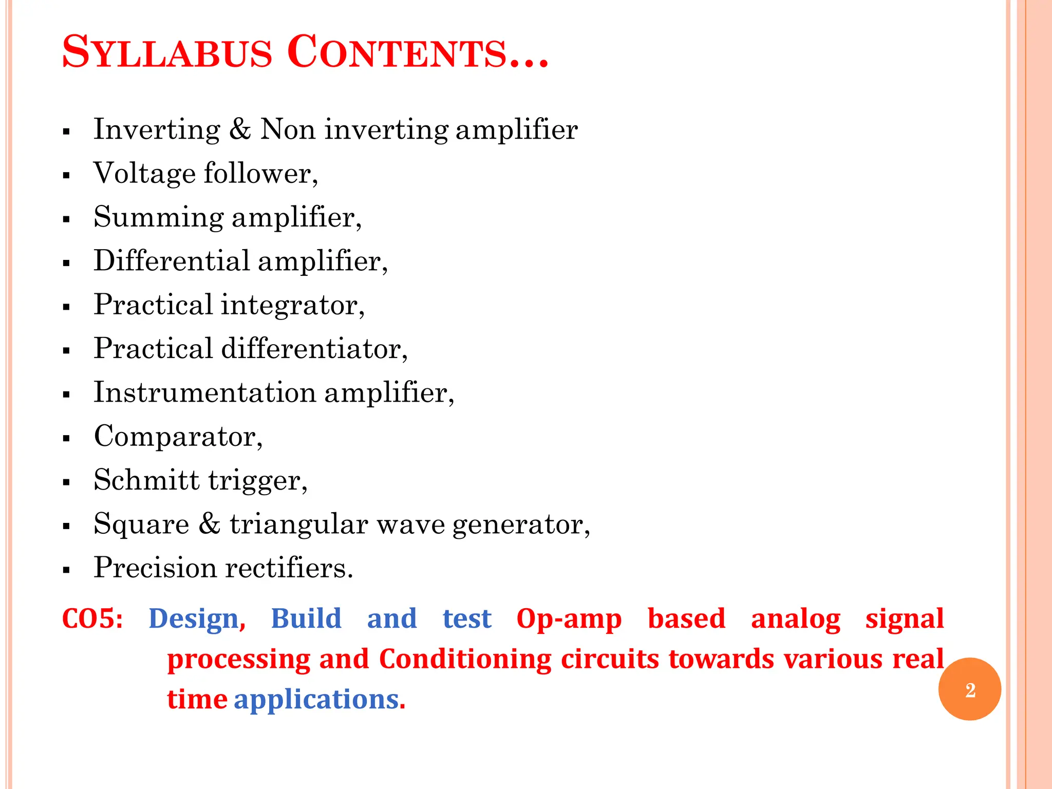
SYLLABUS CONTENTS…
 Inverting & Non inverting amplifier
 Voltage follower,
 Summing amplifier,
 Differential amplifier,
 Practical integrator,
 Practical differentiator,
 Instrumentation amplifier,
 Comparator,
 Schmitt trigger,
 Square & triangular wave generator,
 Precision rectifiers.
CO5: Design, Build and test Op-amp based analog signal
processing and Conditioning circuits towards various real
time applications. 2
TEXT BOOK/ REFERENCE BOOK
 T2: Ramakant A. Gaikwad, “Op Amps and Linear
Integrated Circuits”, Pearson Education 2000.
and Kanchana
Circuits”, Tata
Bhaskaran, “Linear
McGraw Hill, India
 R3: Salivahanan
Integrated
2008
3
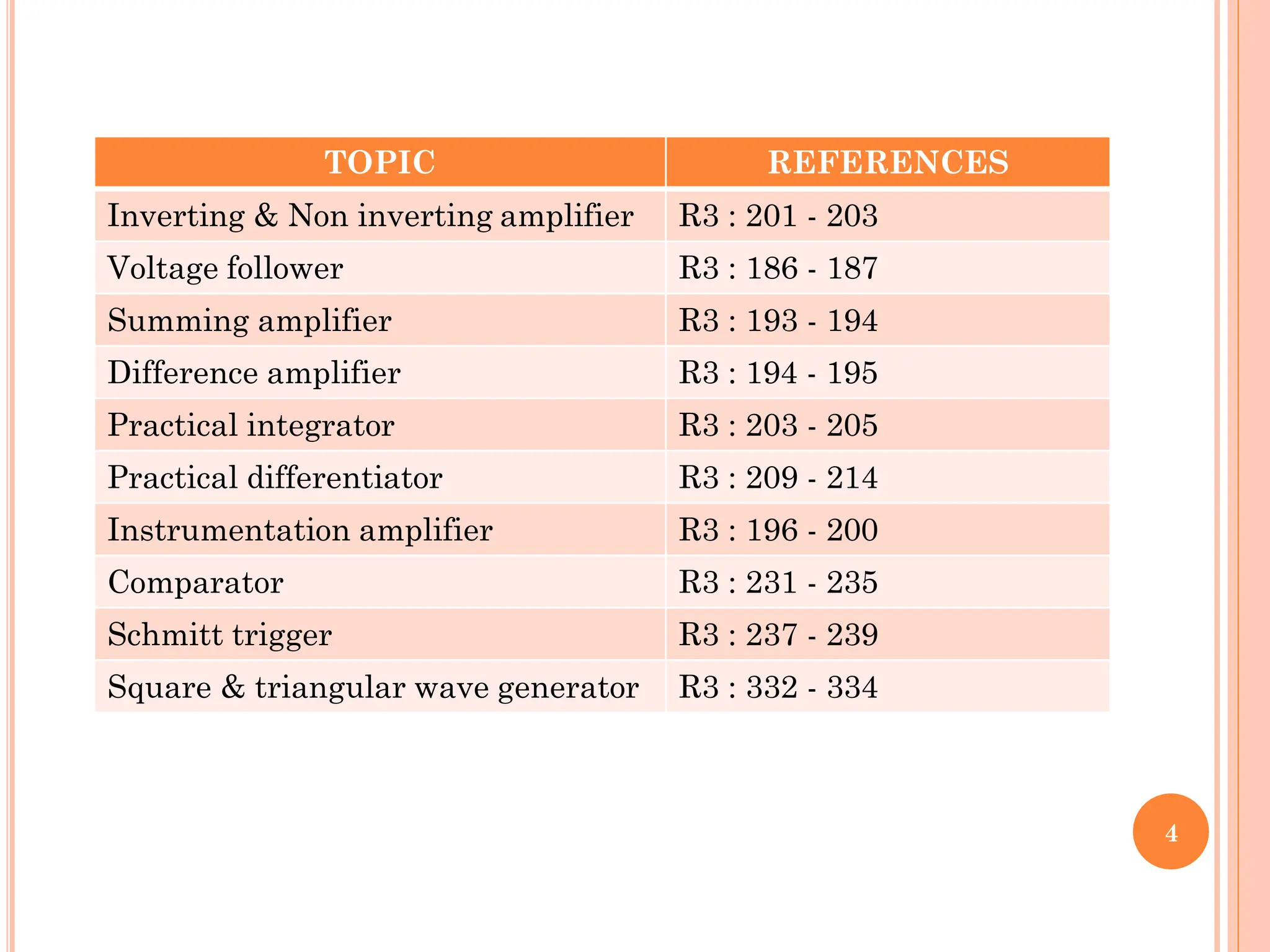
4
TOPIC REFERENCES
Inverting & Non inverting amplifier R3 : 201 - 203
Voltage follower R3 : 186 - 187
Summing amplifier R3 : 193 - 194
Difference amplifier R3 : 194 - 195
Practical integrator R3 : 203 - 205
Practical differentiator R3 : 209 - 214
Instrumentation amplifier R3 : 196 - 200
Comparator R3 : 231 - 235
Schmitt trigger R3 : 237 - 239
Square & triangular wave generator R3 : 332 - 334
LECTURE # 01
 Virtual Ground/ Virtual Short.
 Inverting amplifier.
 Non inverting amplifier.
 Voltage follower.
5
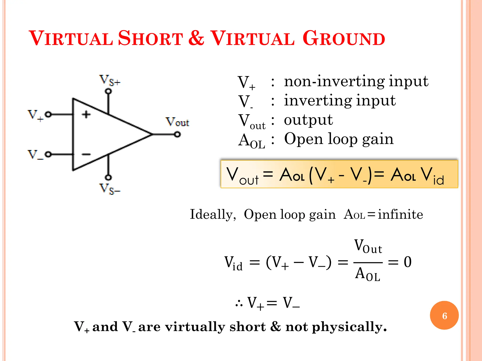
VIRTUAL SHORT & VIRTUAL GROUND
: non-inverting input
: inverting input
V+
V-
Vout : output
AOL : Open loop gain
Vout = AOL (V+ - V-)= AOL Vid
Ideally, Open loop gain AOL = infinite
id
AOL
VOut
V = V+ − V− = = 0
∴ V+= V−
V+ and V- are virtually short & not physically.
6
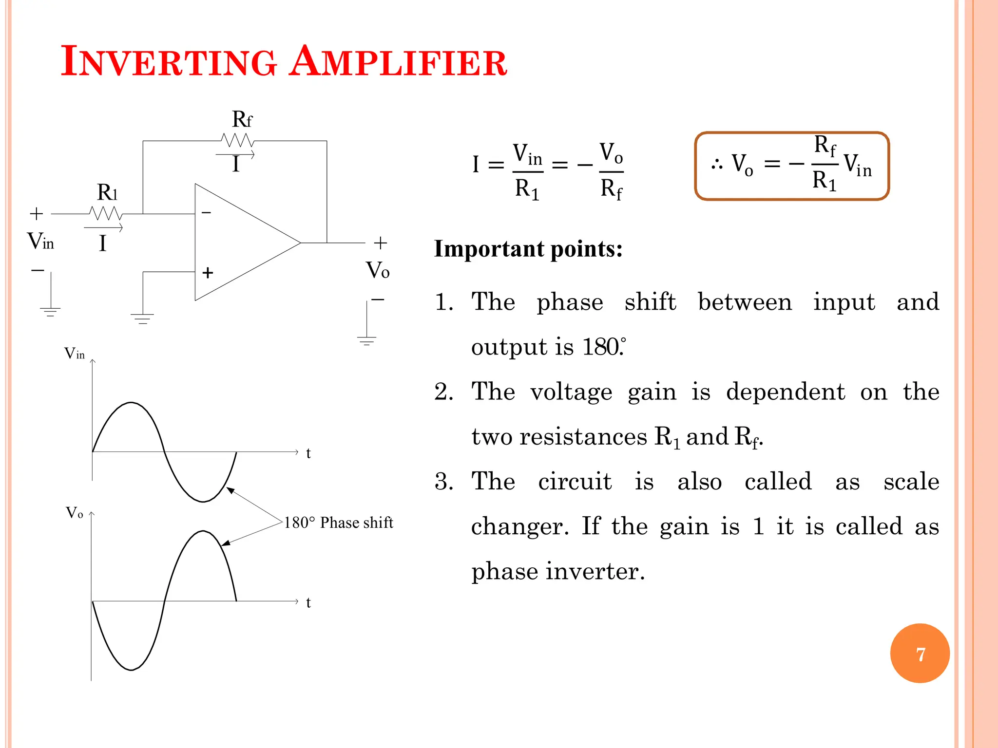
INVERTING AMPLIFIER
+
_
Vin
Rf
R1
Vo
+
_
_
+
I
Vin Vo
I I = = −
R R
1 f
o
∴ V = −
Rf
R1
Vin
Vin
Vo
t
t
180° Phase shift
Important points:
1. The phase shift between input and
output is 180.̊
2. The voltage gain is dependent on the
two resistances R1 and Rf.
3. The circuit is also called as scale
changer. If the gain is 1 it is called as
phase inverter.
7
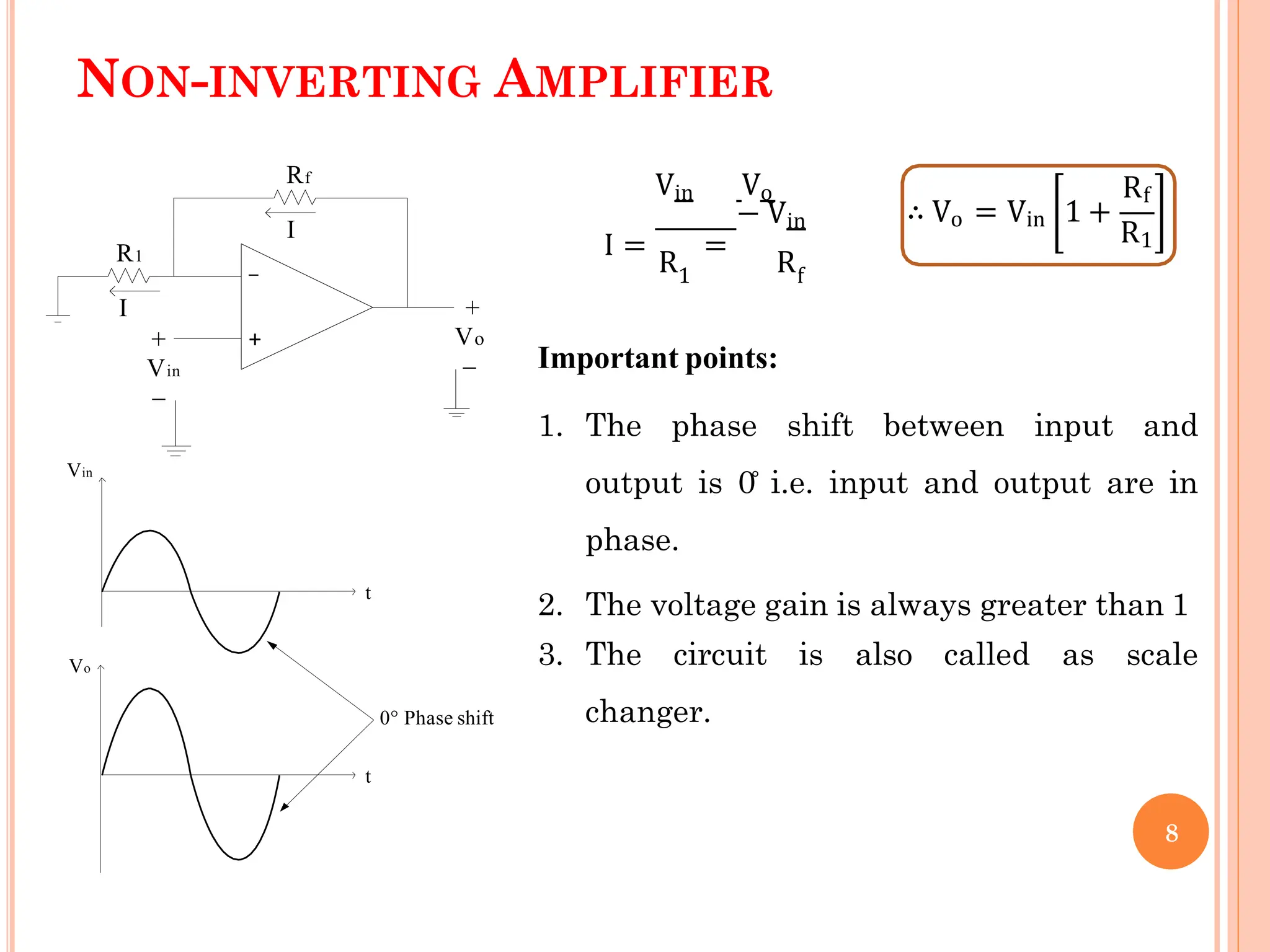
NON-INVERTING AMPLIFIER
Vin Vo
− Vin
I =
R
=
R
1 f
∴ Vo = Vin 1 +
Rf
R1
Important points:
1. The phase shift between input and
output is 0̊ i.e. input and output are in
phase.
2. The voltage gain is always greater than 1
3. The circuit is also called as scale
changer.
+
_
Rf
R1
Vo
+
_
_
+
I
I
Vin
Vin
Vo
t
t
0° Phase shift
8
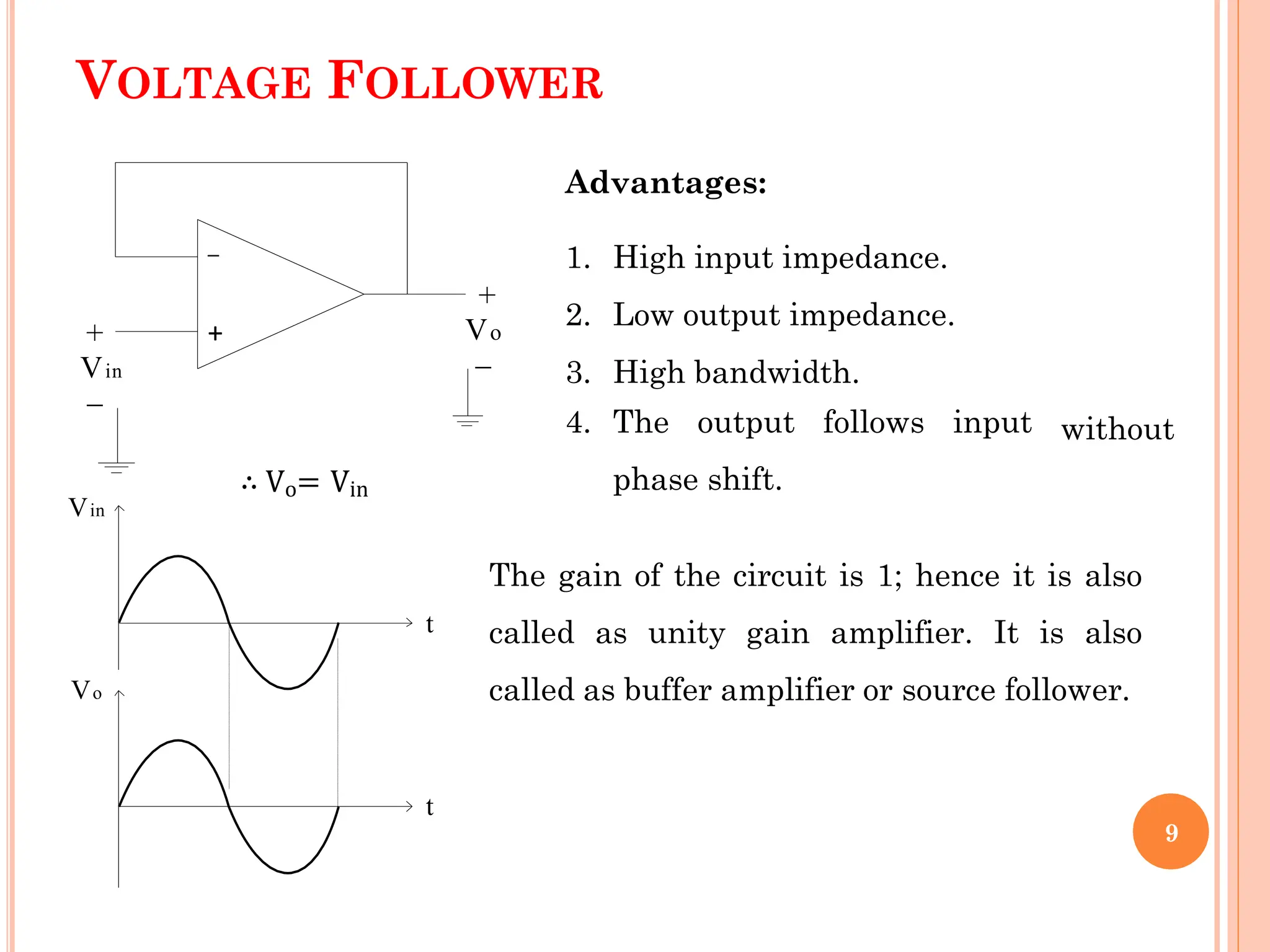
VOLTAGE FOLLOWER
+
_
Vo
+
_
_
+
Vin
∴ Vo= Vin
The gain of the circuit is 1; hence it is also
called as unity gain amplifier. It is also
called as buffer amplifier or source follower.
Vin
Vo
t
t
Advantages:
without
1. High input impedance.
2. Low output impedance.
3. High bandwidth.
4. The output follows input
phase shift.
9
LECTURE # 02
 Summing Amplifier [2 Input]
Inverting & Noninverting Type
 Difference Amplifier [ Subtractor]
10
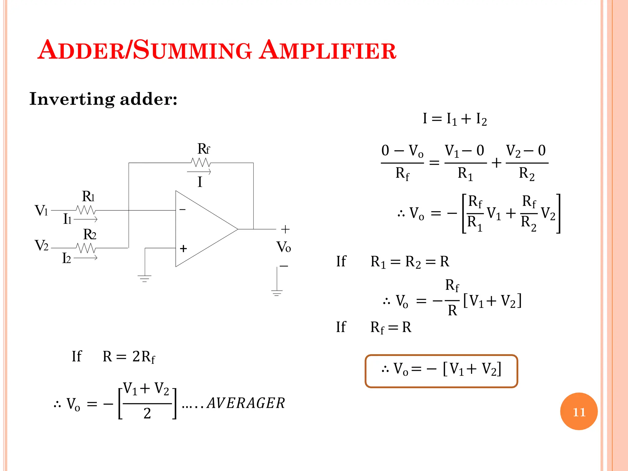
ADDER/SUMMING AMPLIFIER
Inverting adder:
+
_
Rf
R1
Vo
+
_
I
V1
V2
R2
I1
I2
I = I1 + I2
R
=
0 − Vo V1− 0
R
f 1
+
V2− 0
R2
1
Rf Rf
2
∴ Vo = −
R
V1 +
R
V2
If R1 = R2 = R
o
R
Rf
∴ V = − V1+ V2
If Rf = R
∴ Vo = − V1+ V2
If R = 2Rf
o
V1+ V2
∴ V = −
2
…. . 𝐴𝑉𝐸𝑅𝐴𝐺𝐸𝑅
11
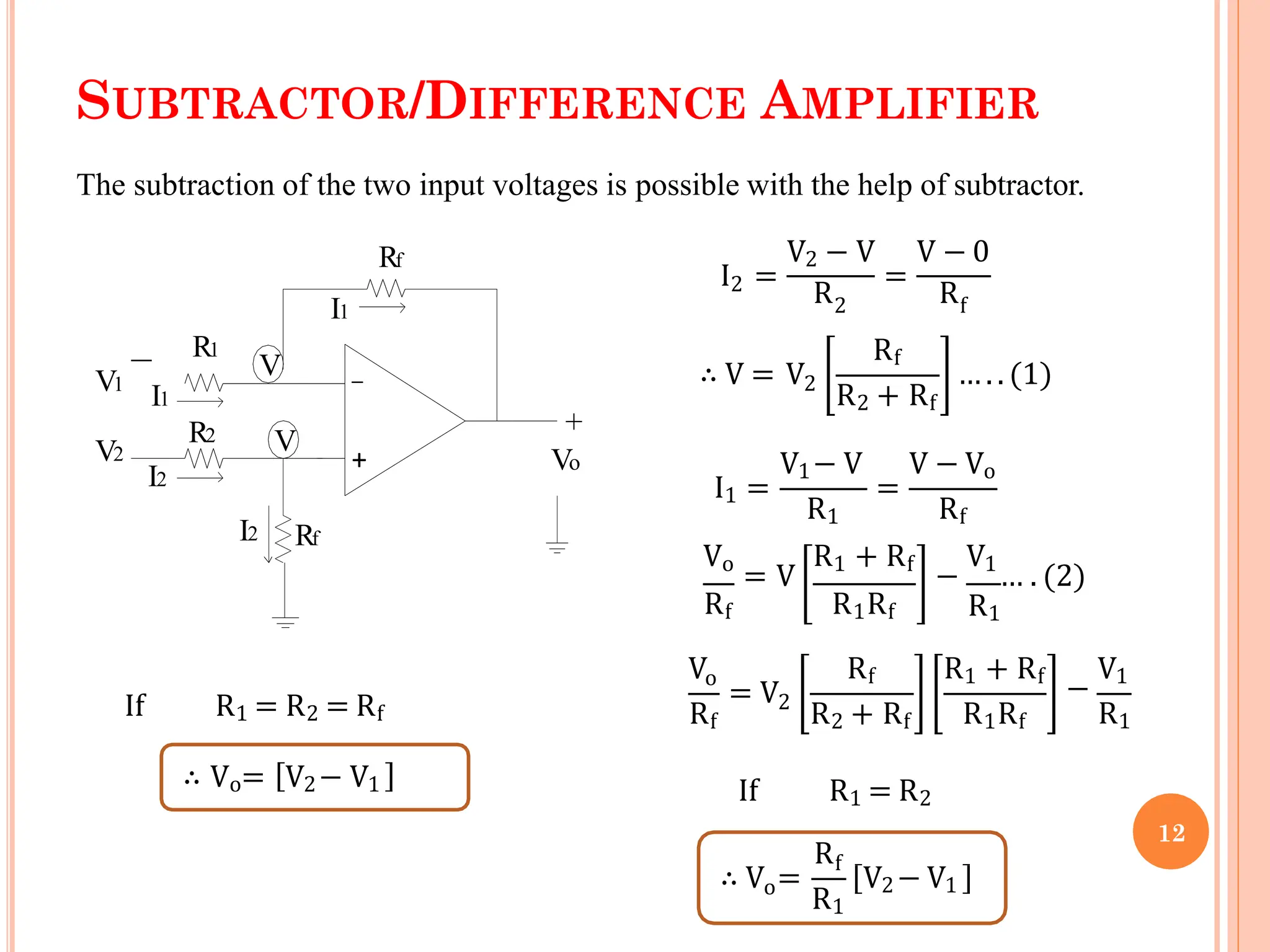
SUBTRACTOR/DIFFERENCE AMPLIFIER
+
+
_
Rf
Rf
R2
V1
V2 Vo
R1
I1
I1
I2
I2
V
V
The subtraction of the two input voltages is possible with the help of subtractor.
2
V2 − V V − 0
I =
R
=
R
2 f
∴ V = V2
Rf
R2 + Rf
…. . (1)
I1 =
V1− V
R1
=
V − Vo
Rf
Rf
Vo
= V
R1 + Rf
−
V1
… . (2)
R1
Vo
Rf
= V2
R2 + Rf R1Rf
R1Rf
Rf R1 + Rf
−
V1
R1
If R1 = R2
o
∴ V =
Rf
R1
V2− V1
If R1 = R2 = Rf
∴ Vo= V2− V1
12
LECTURE # 03
 Basic/Ideal Integrator-
 Circuit Diagram, Output equation
 Response to Step, Square and Sinewave inputs
 Frequency Response.
 Drawbacks of Ideal Integrator.
13
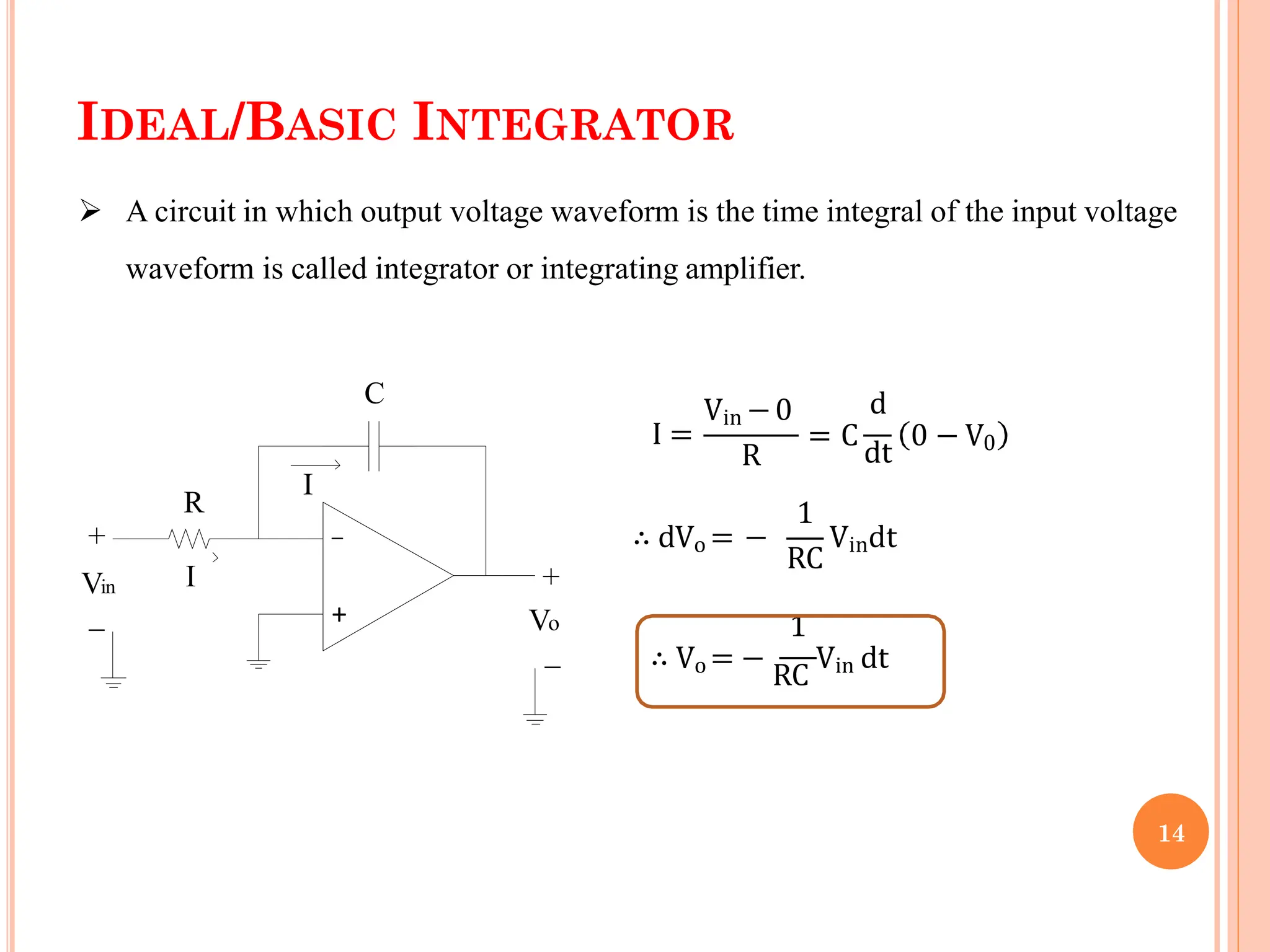
IDEAL/BASIC INTEGRATOR
 A circuit in which output voltage waveform is the time integral of the input voltage
waveform is called integrator or integrating amplifier.
+
_
Vin
+
_
+
_
Vo
C
R
I
I
I =
Vin −0
R
d
= C
dt
0 − V0
∴ dVo = −
1
RC
Vindt
1
∴ Vo = −
RC
Vin dt
14
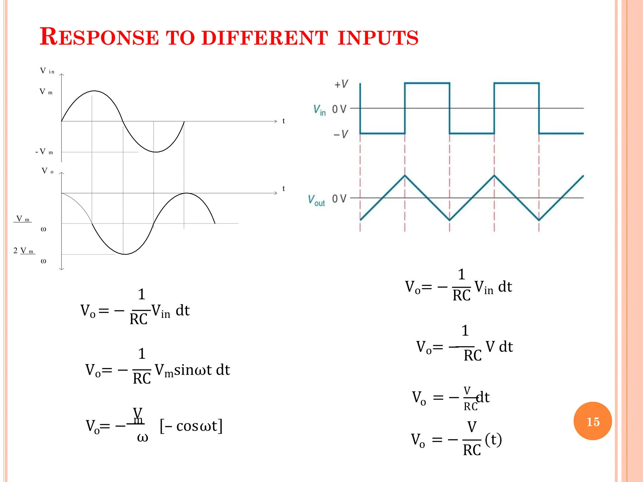
RESPONSE TO DIFFERENT INPUTS
t
t
V m
ω
2 V m
ω
V i n
V m
- V m
V o
1
Vo = −
RC
Vin dt
1
Vo= −
RC
Vmsinωt dt
o
V
V = − m
ω
– cosωt
1
Vo= −
RC
Vin dt
1
Vo= −
RC
V dt
Vo = − V
dt
o
V = −
RC
V
RC
t
15
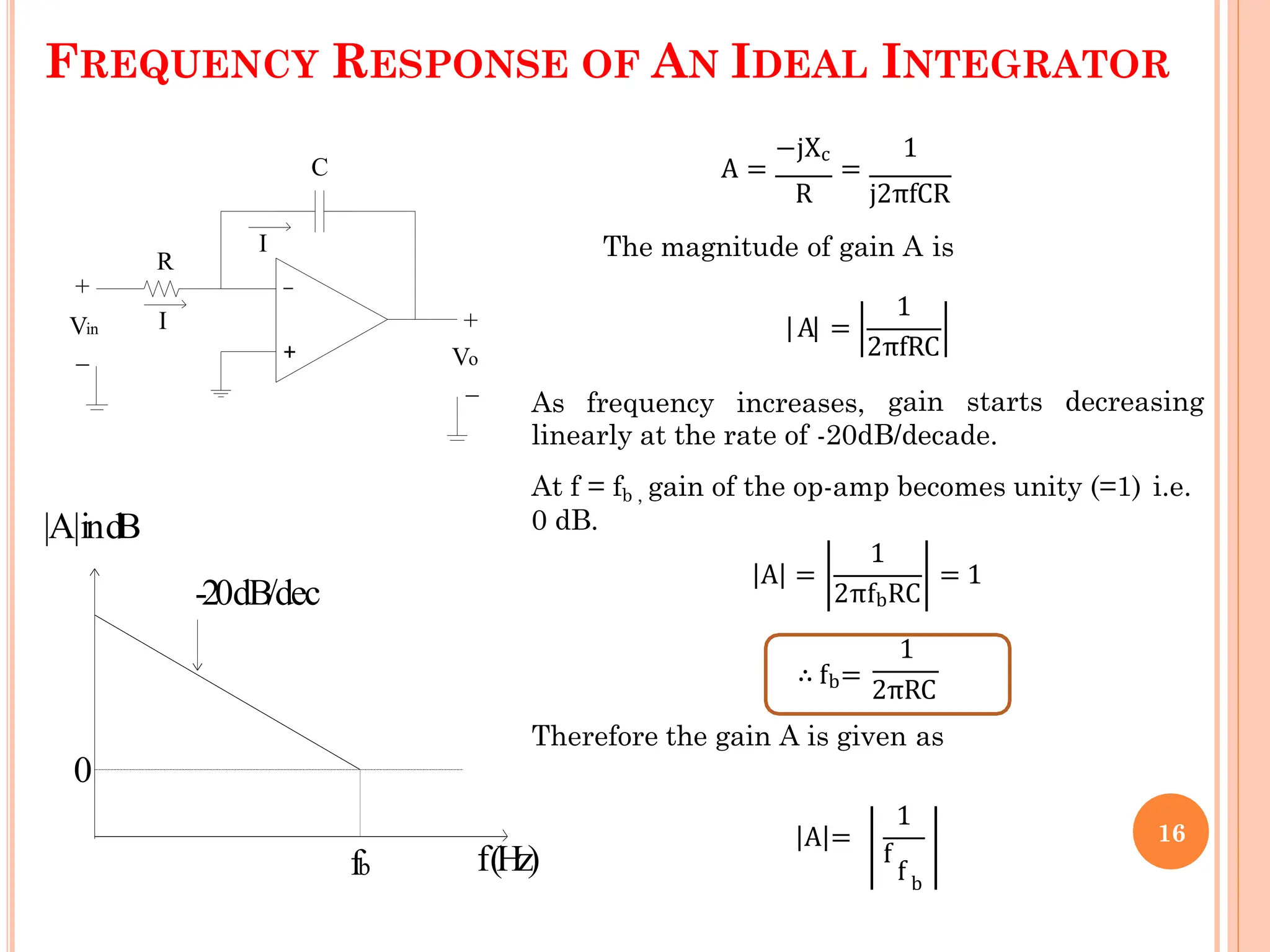
FREQUENCY RESPONSE OF AN IDEAL INTEGRATOR
+
_
Vin
+
+
_
_ Vo
C
R
I
I
−jXc 1
A = =
R j2πfCR
The magnitude of gain A is
1
A =
As frequency increases,
2πfRC
gain starts decreasing
linearly at the rate of -20dB/decade.
At f = fb , gain of the op-amp becomes unity (=1) i.e.
0 dB.
1
2πfbRC
A = = 1
1
∴ fb=
2πRC
Therefore the gain A is given as
A =
1
f
f b
f(Hz)
|A|indB
0
-20dB/dec
fb
16
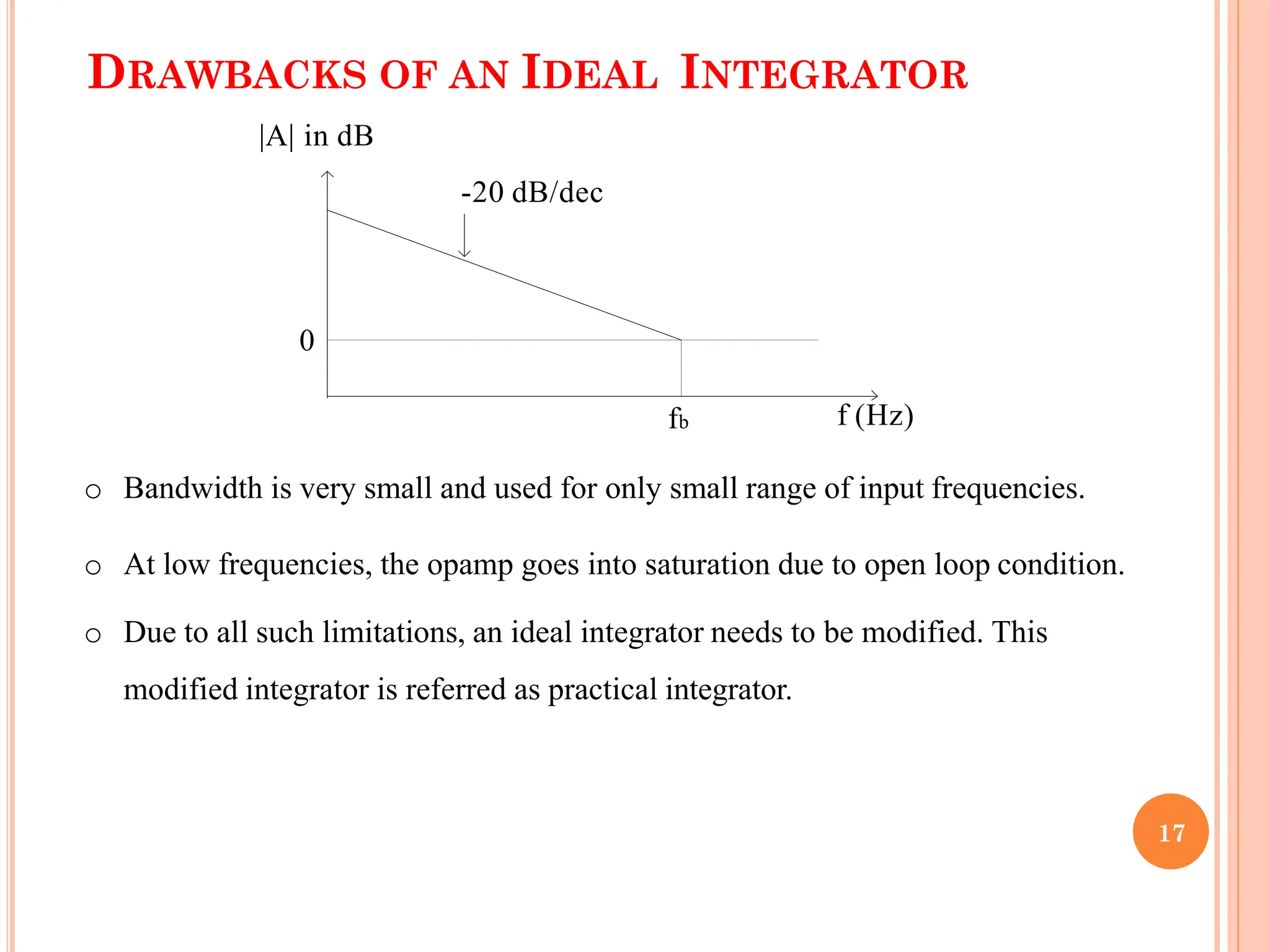
DRAWBACKS OF AN IDEAL INTEGRATOR
o Bandwidth is very small and used for only small range of input frequencies.
o At low frequencies, the opamp goes into saturation due to open loop condition.
o Due to all such limitations, an ideal integrator needs to be modified. This
modified integrator is referred as practical integrator.
f (Hz)
0
|A| in dB
-20 dB/dec
fb
17
LECTURE # 04
 Practical Integrator- Circuit Diagram
 Frequency Response and related observations.
 Design Considerations.
 How the Problems in ideal integrator are overcome
in practical integrator.
 Design equations and Problems.
18
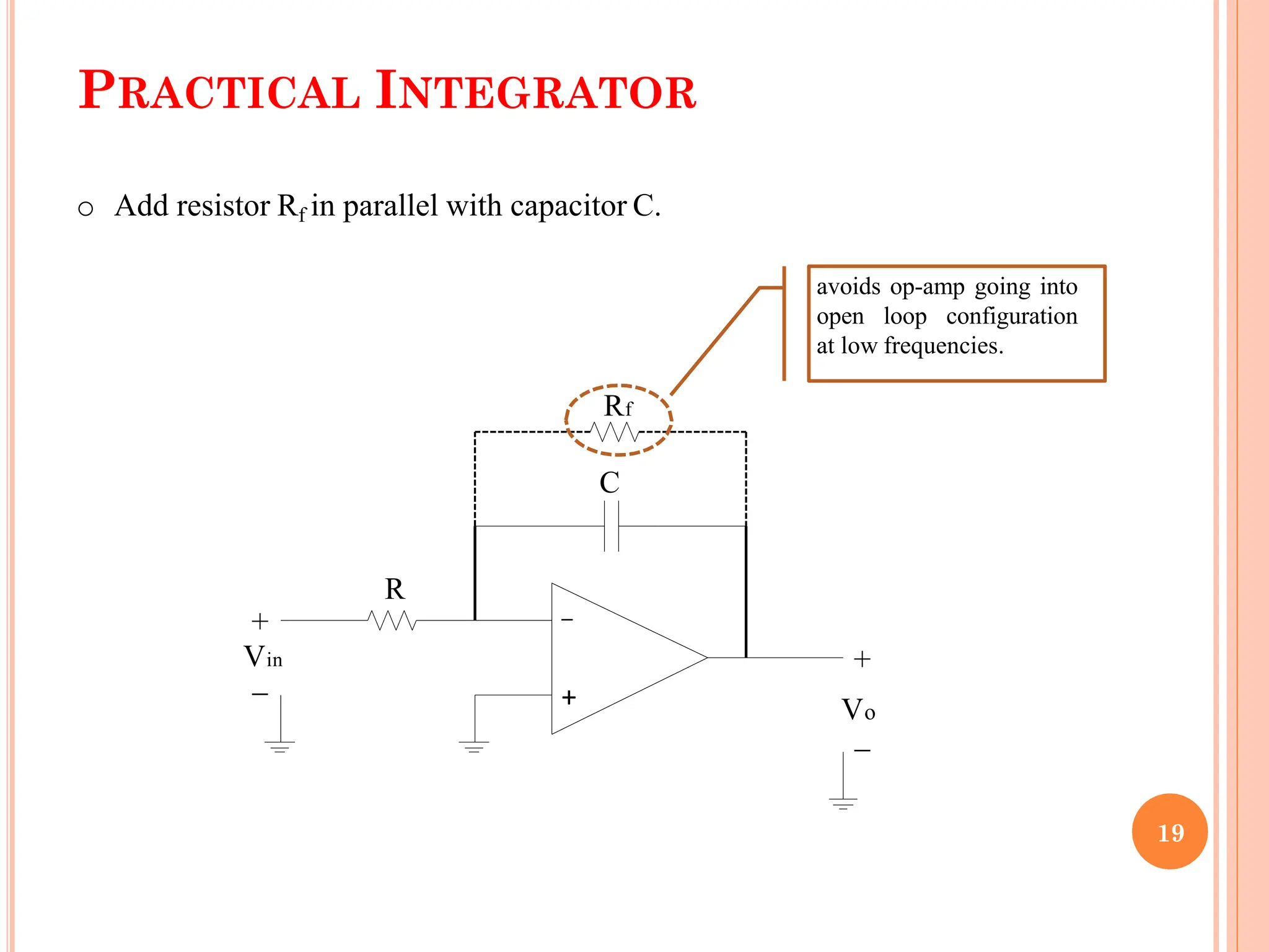
PRACTICAL INTEGRATOR
R
Vin
+
_
Vo
Rf
C
+
_
_
+
o Add resistor Rf in parallel with capacitor C.
avoids op-amp going into
open loop configuration
at low frequencies.
19
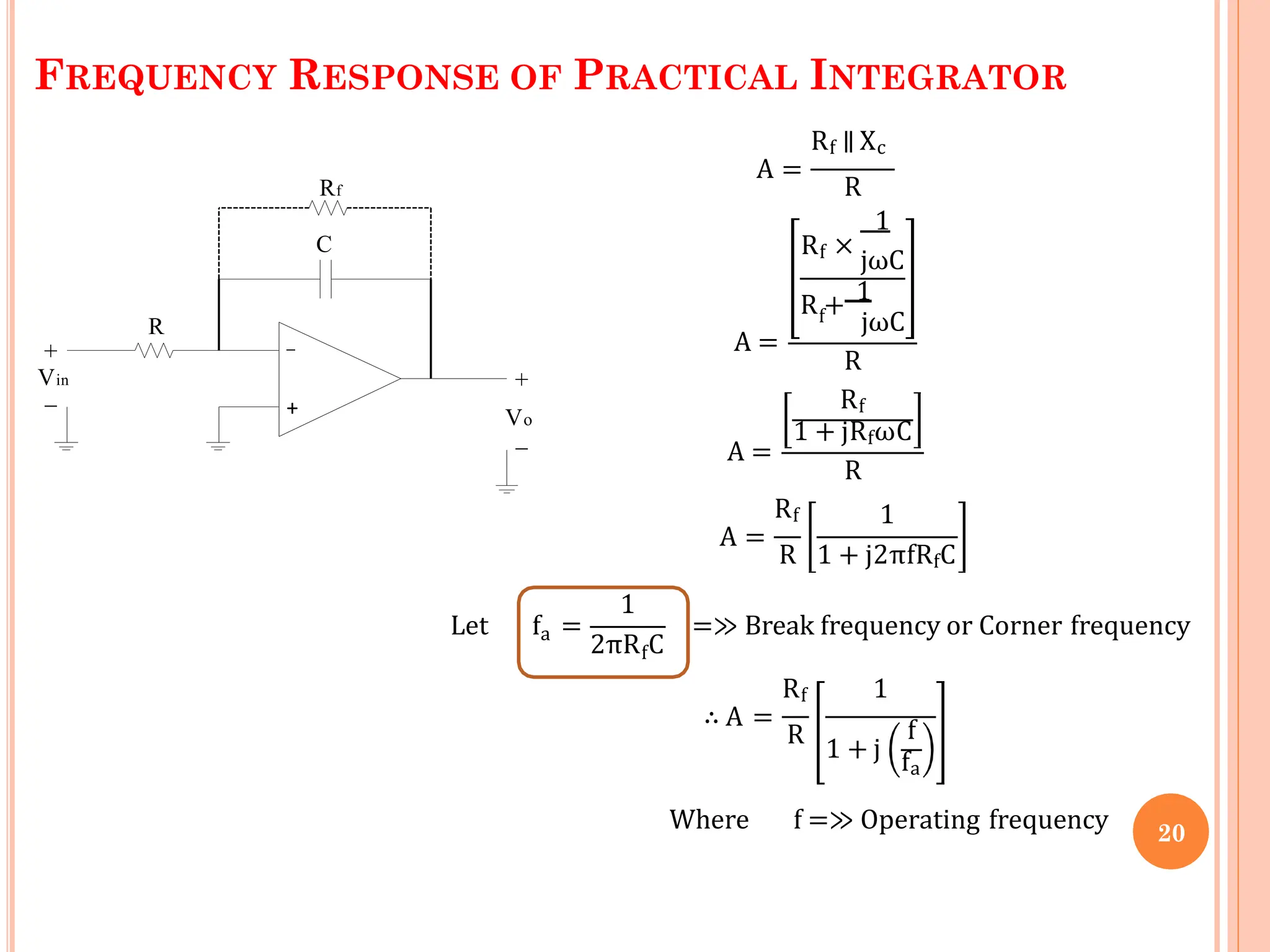
FREQUENCY RESPONSE OF PRACTICAL INTEGRATOR
Rf ∥ Xc
A =
R
A =
1
Rf ×
jωC
f
R + 1
jωC
A =
R
Rf
1 + jRfωC
R
Rf
A =
1
R 1 + j2πfRfC
a
Let f =
1
f
2πR C
=≫ Break frequency or Corner frequency
R
Rf 1
∴ A =
1 + j
f
fa
Where f =≫ Operating frequency
R
Rf
Vin
+
_
Vo
C
+
_
_
+
20
A =
Rf
R
1
1 +
f
fa
2
 Consider the following cases:
1. When f = 0 , the gain A =
Rf
R
−−−− −dc gain
2. When a
0 < 𝑓 < f , the gain A ≅
Rf
R
a
3. When f > f , the gain A ≪
Rf
R
a
4. When f = f , the gain A =
Rf 1
R 2
A = 0.707
Rf
R
fa
|A| in dB
0
-20 dB/dec
fb f (Hz)
Rf
R
-3 dB
[DC gain] 20 log10
True integration is possible over the range
fa < 𝑓 <fb
For better integration fb ≥ 10fa
21
Prob: Design a practical integrator using Op-Amp IC 741C to satisfy the following
specifications. Assume Vcc = +15V.
1) 3-dB cut-off frequency = 1.5 kHz 2) DC gain = 10
Sketch the frequency response of the circuit.
Sol:
Rf
Given: fa = 1.5 KHz , DC gain = R
= 10
a
f =
1
2πR C
Let
f
C = 0.1µf
∴ 𝐑𝐟 = 𝟏. 𝟎𝟔𝟏𝐤Ω
R
Rf
DC gain = = 10
DC gain = 20log 10
Rf
R
= 20dB
b
f =
fb = 10fa =15kHz
1
2πRC
∴ 𝐑 = 𝟏𝟎𝟔. 𝟏𝟎 Ω
𝐑𝐎𝐌 = 𝐑 ∥ 𝐑𝐟 = 96.4545 Ω
|A| in dB
0
-20 dB/dec
Rf
R
-3 dB
[DC gain] 20 log10
R
Vin
+
_
Rf
C
+
Vo
_
_
+
22
fa fb f (Hz)
LECTURE # 05
 Basic/Ideal Differentiator-
 Circuit Diagram, Output equation
 Response to Step, Square and Sinewave inputs
 Frequency Response.
 Drawbacks of Ideal Differentiator.
23
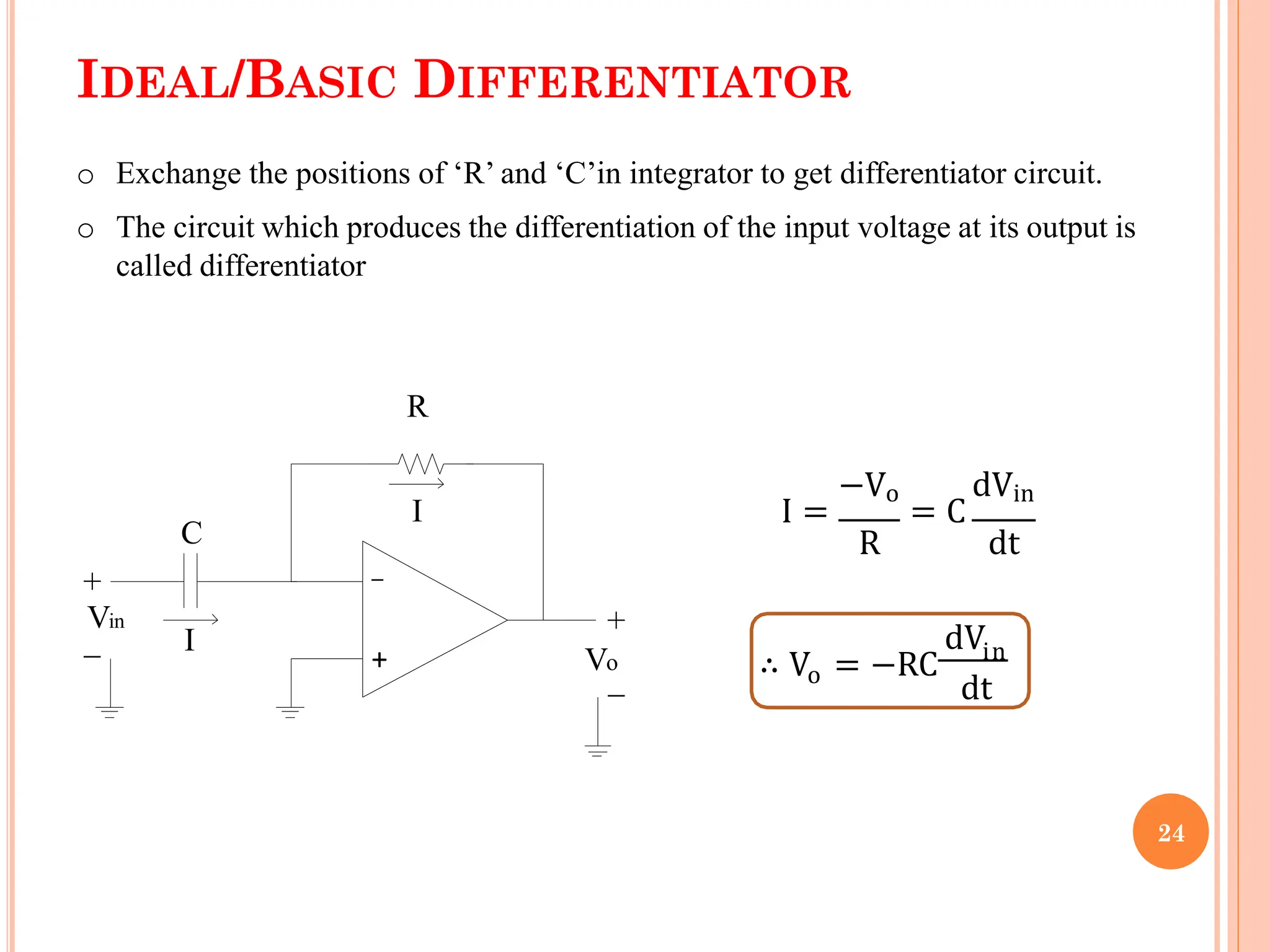
IDEAL/BASIC DIFFERENTIATOR
o Exchange the positions of ‘R’ and ‘C’in integrator to get differentiator circuit.
o The circuit which produces the differentiation of the input voltage at its output is
called differentiator
+
_
+
_
C
R
Vin
_
+
Vo
I
I
−Vo dVin
I = = C
R dt
o
dV
∴ V = −RC in
dt
24
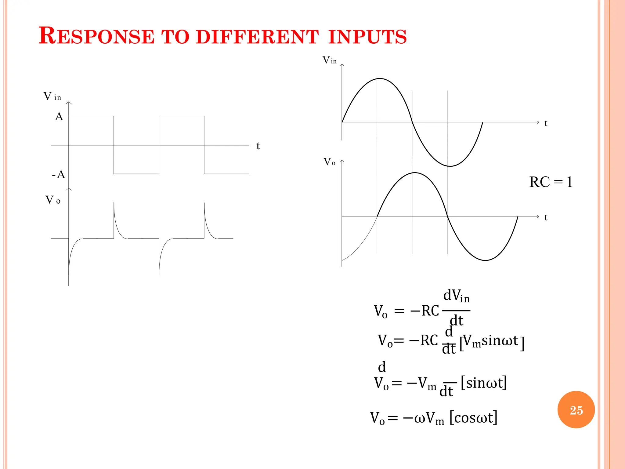
RESPONSE TO DIFFERENT INPUTS
t
V o
V in
A
-A
Vin
Vo
t
t
o
dVin
V = −RC
dt
d
Vo= −RC
dt
Vmsinωt
d
Vo = −Vm
dt
sinωt
Vo = −ωVm cosωt
RC = 1
25
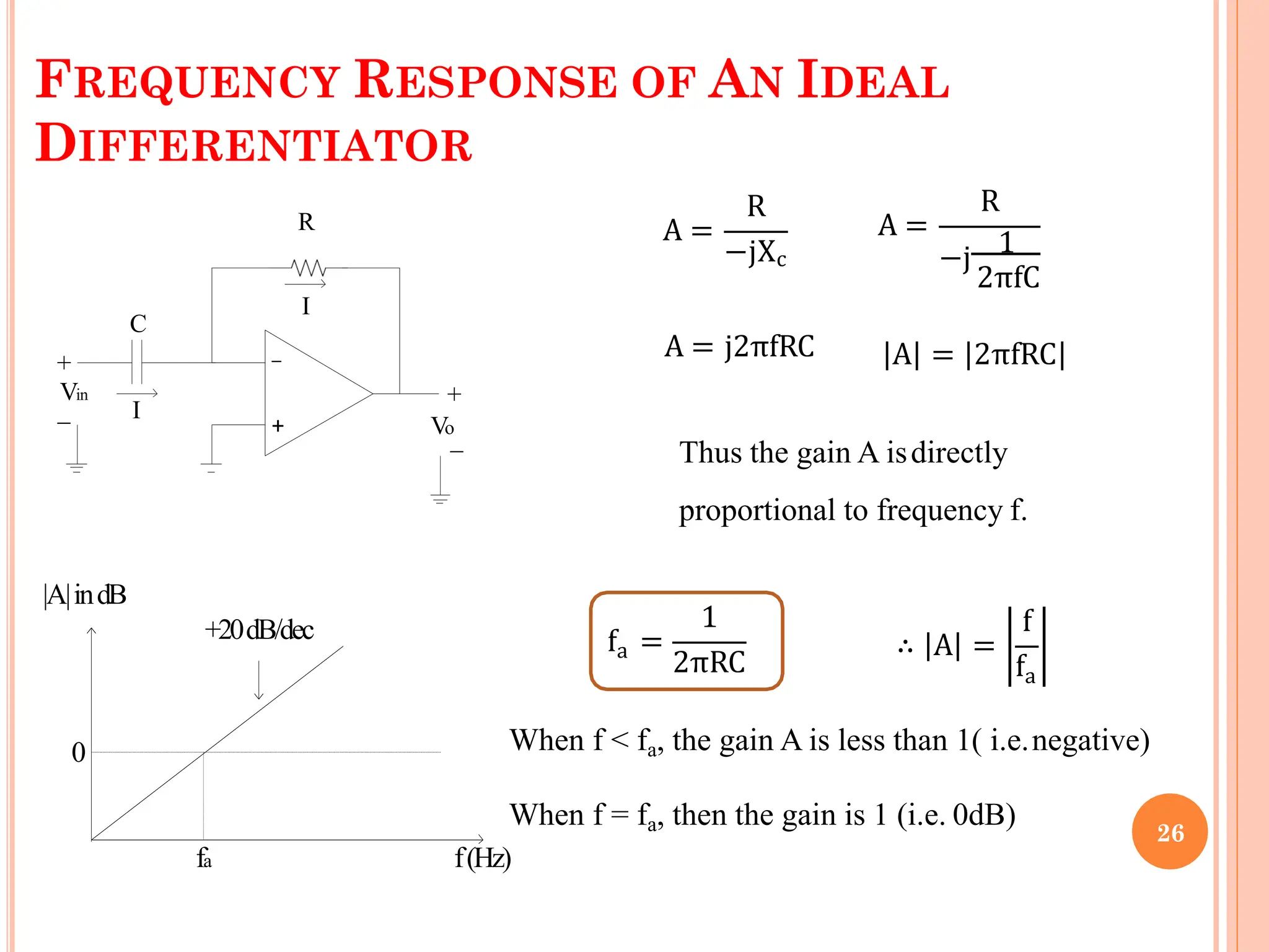
FREQUENCY RESPONSE OF AN IDEAL
DIFFERENTIATOR
+
_
+
_
C
R
Vin +
Vo
_
I
I
A =
R
−jXc
A =
R
−j 1
2πfC
A = j2πfRC A = 2πfRC
Thus the gain A isdirectly
proportional to frequency f.
fa f(Hz)
|A|indB
0
+20dB/dec
a
f =
1
2πRC
∴ A =
f
fa
When f < fa, the gain A is less than 1( i.e.negative)
When f = fa, then the gain is 1 (i.e. 0dB)
26
DRAWBACKS OF AN IDEAL DIFFERENTIATOR
o Unstable at high frequencies.[Op-Amp may go into saturation]
o Much Sensitive to noise at high frequencies leading to mis-
amplification of the signal..
The reactance of the capacitor Xc is givenas
1
Xc =
2πfC
As frequency increases, Xc reduces i.e. Capacitor draws more
current from input source.
27
LECTURE # 06
 Practical differentiator- Circuit Diagram
 Frequency Response and related observations.
 Design Considerations.
 How the Problems in ideal differentiator are overcome
in practical differentiator.
 Design equations and Problems.
28
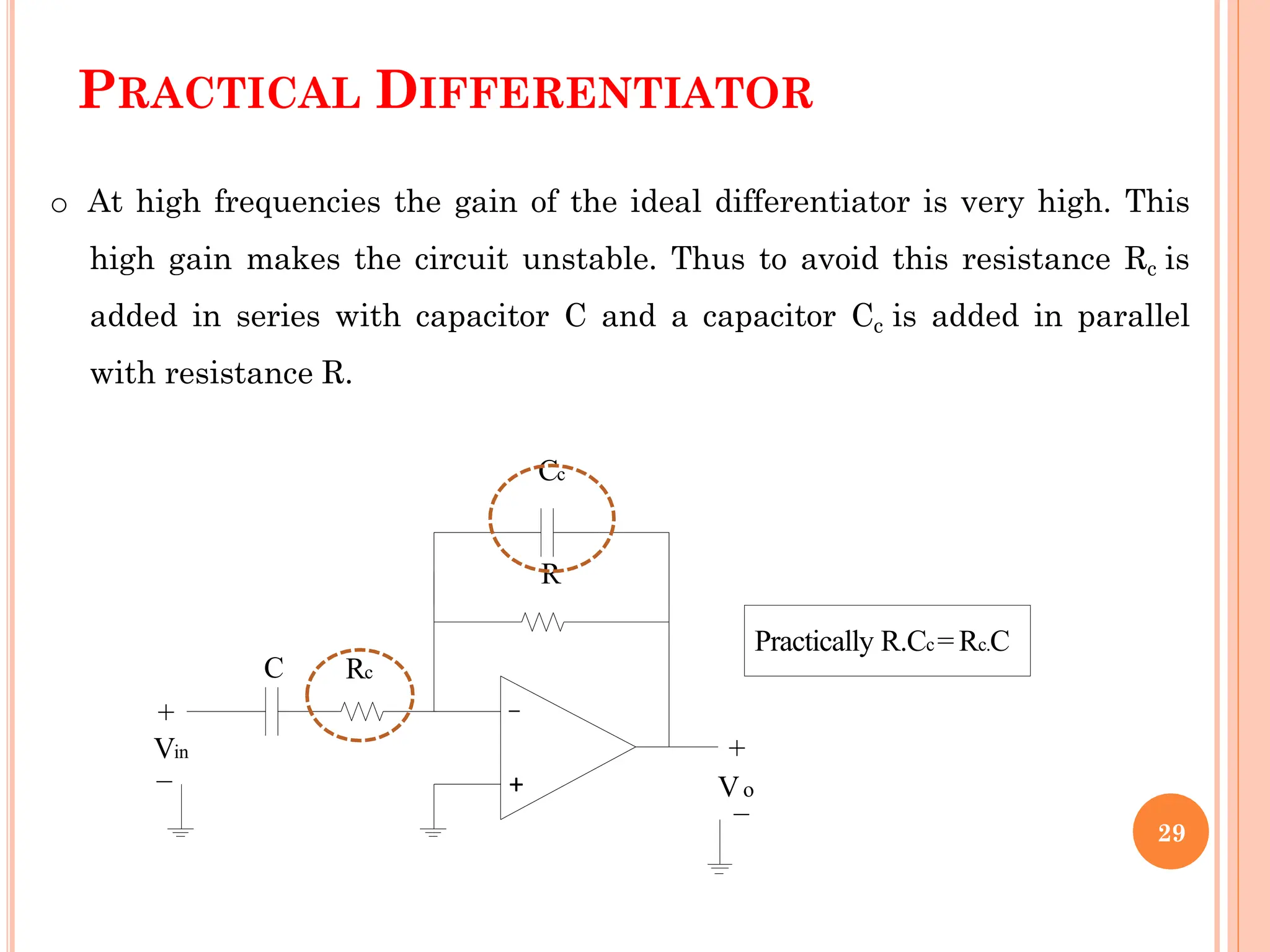
PRACTICAL DIFFERENTIATOR
+
_
+
V_o
C
o At high frequencies the gain of the ideal differentiator is very high. This
high gain makes the circuit unstable. Thus to avoid this resistance Rc is
added in series with capacitor C and a capacitor Cc is added in parallel
with resistance R.
Cc
R
Rc
Vin
+
_
Practically R.Cc= Rc.C
29
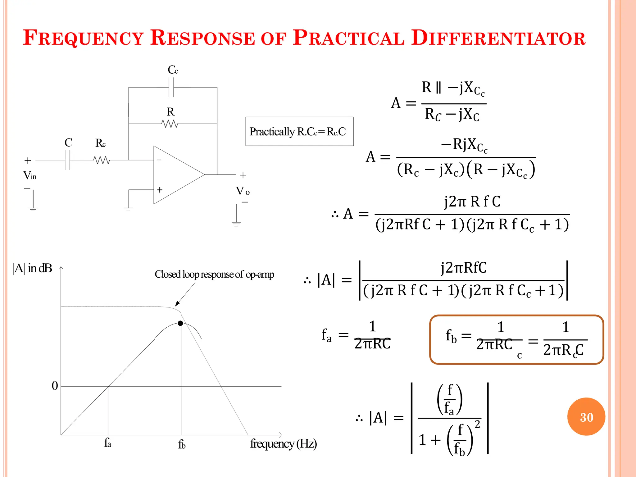
FREQUENCY RESPONSE OF PRACTICAL DIFFERENTIATOR
R ∥ −jXCc
A =
R𝐶 −jXC
+
_
+
V_o
Cc
R
C Rc
Vin
+
_
Practically R.Cc=Rc.C
A =
∴ A =
−RjXCc
Rc − jXc R − jXCc
j2π R f C
c
j2πRf C + 1 j2π R f C + 1
∴ A =
j2πRfC
j2π R f C + 1 j2π R f Cc +1
1 1
fa =
2πRC
fb =
2πRC
c
1
c
=
2πR C
∴ A =
f
fa
1 +
f
fb
2
fb
fa
0
|A| indB
frequency(Hz)
Closedloopresponseof op-amp
.
30
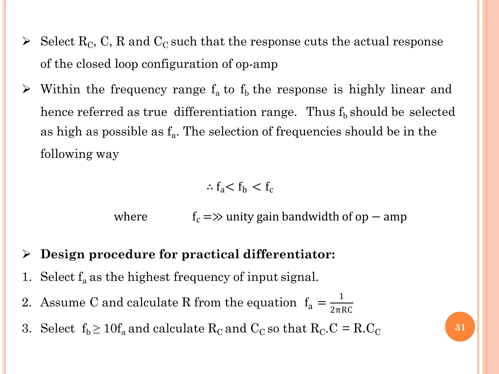
 Select RC, C, R and CC such that the response cuts the actual response
of the closed loop configuration of op-amp
 Within the frequency range fa to fb the response is highly linear and
hence referred as true differentiation range. Thus fb should be selected
as high as possible as fa. The selection of frequencies should be in the
following way
∴ fa< fb < fc
where fc =≫ unity gain bandwidth of op − amp
 Design procedure for practical differentiator:
1. Select fa as the highest frequency of input signal.
a
2. Assume C and calculate R from the equation f =
1
2πRC
3. Select fb ≥ 10fa and calculate RC and CC so that RC.C = R.CC
31
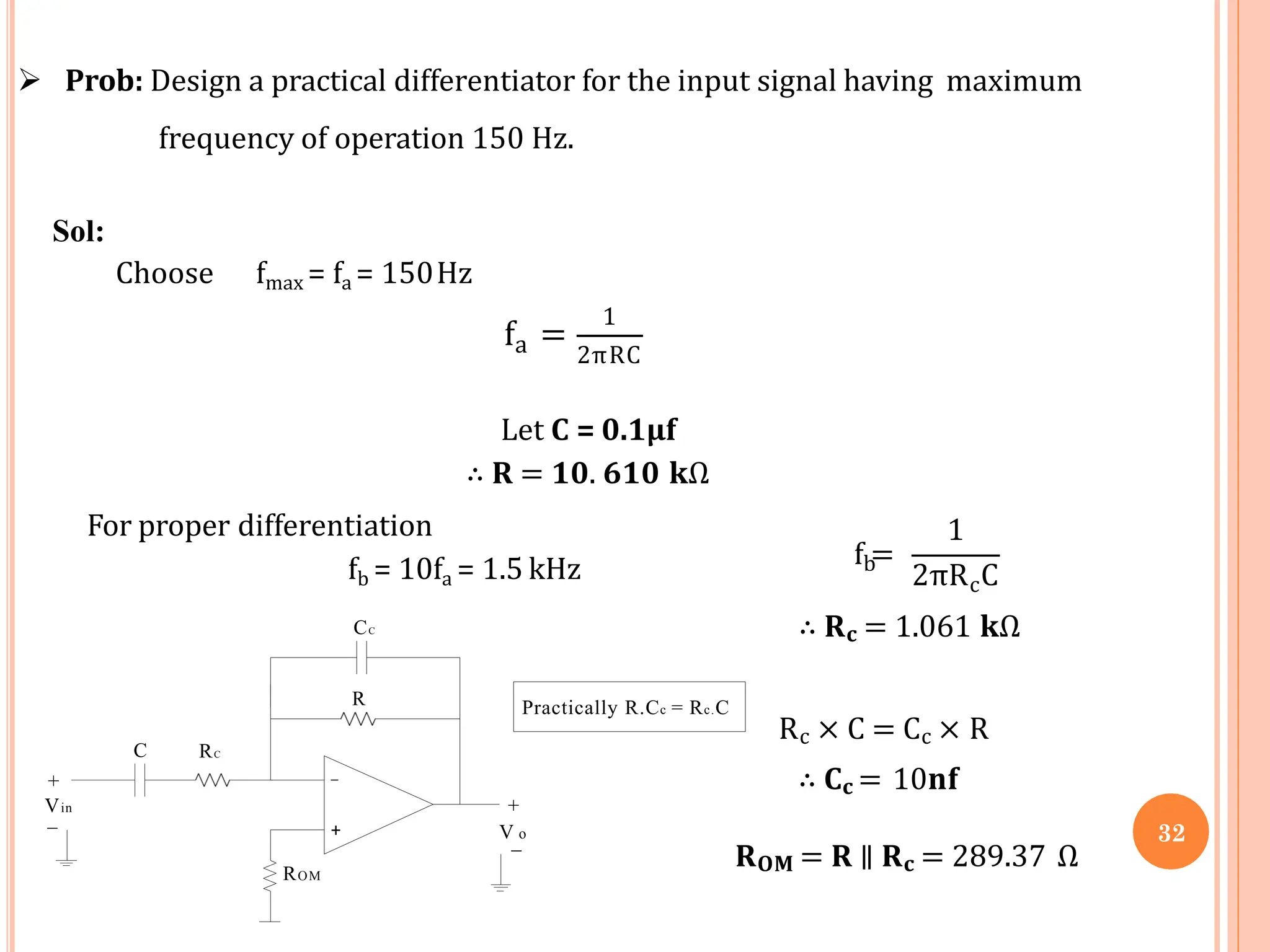
 Prob: Design a practical differentiator for the input signal having maximum
frequency of operation 150 Hz.
Sol:
Choose fmax = fa = 150Hz
a
f =
1
2πRC
Let C = 0.1µf
∴ 𝐑 = 𝟏𝟎. 𝟔𝟏𝟎 𝐤Ω
b
f =
1
c
2πR C
∴ 𝐑𝐜 = 1.061 𝐤Ω
Rc × C = Cc × R
∴ 𝐂𝐜 = 10𝐧𝐟
𝐑𝐎𝐌 = 𝐑 ∥ 𝐑𝐜 = 289.37 Ω
+
_
+
V_o
C
For proper differentiation
fb = 10fa = 1.5 kHz
CC
R
RC
Vin
+
_
ROM
Practically R.Cc = Rc.C
32
LECTURE # 07
 Introduction and Significance.
 Characteristics of Good Inst. Amplifier
 3 Op-Amp Instrumentation Amplifier
 Derivation of Output Voltage.
 Problems based on equation.
33
WHAT IS INSTRUMENTATION AMPLIFIER
o To amplify the low level output signal of a transducer so that it
can drive the indicator or display is a measure function of an
instrumentation amplifier.
o The instrumentation amplifier is used for precise low level
signal amplification where low noise, low thermal drift and
high input resistance are required.
o Besides this low power consumption, high CMRR and high
slew rate are desirable for superior performance.
34
REQUIREMENTS OF TYPICAL
INSTRUMENTATION AMPLIFIER SYSTEM
 Differential input arrangement.
 Single ended output.
 Adjustable gain.
 High Input Resistance
 High CMRR
 High Slew Rate
 Low Power Dissipation.
 Low offset & thermal drift.
35
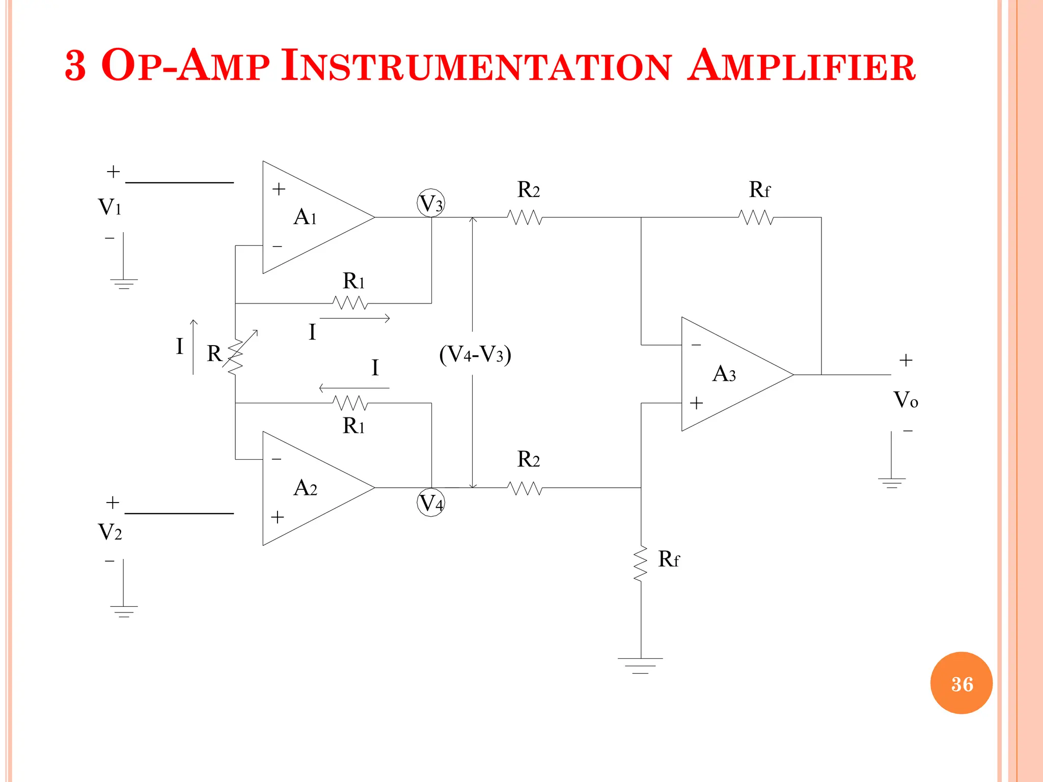
3 OP-AMP INSTRUMENTATION AMPLIFIER
+
+
+
_
_
_ _
_
R
R1
R1
R2
R2
Rf
Rf
+
Vo
_
+
V1
+
V2
V3
V4
A1
A3
A2
I
I
I
(V4-V3)
36
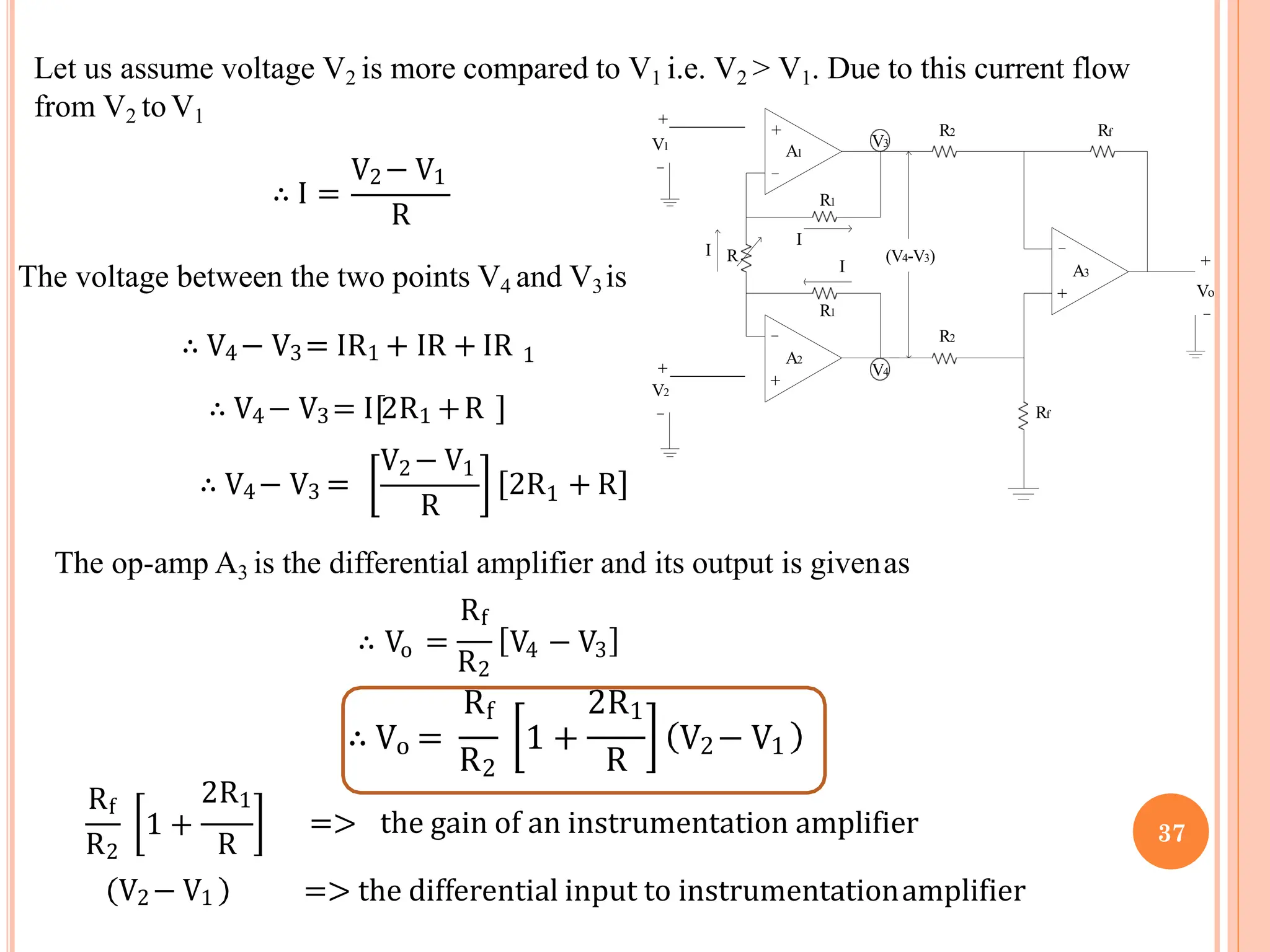
Let us assume voltage V2 is more compared to V1 i.e. V2 > V1. Due to this current flow
from V2 toV1
∴ I =
V2− V1
R
1
∴ V4− V3= IR1 + IR + IR
∴ V4− V3= I 2R1 +R
The voltage between the two points V4 and V3is
∴ V4− V3 =
V2− V1
R 1
2R + R
The op-amp A3 is the differential amplifier and its output is givenas
o
R2
Rf
∴ V = V − V
4 3
Rf
∴ Vo =
R2 R
2R1
1 + V2− V1
Rf
R2
2R1
1 +
R
V2− V1
=> the gain of an instrumentation amplifier
=> the differential input to instrumentationamplifier
+
+
+
_
_
_
_
R
R1
R1
R2
+ R2 Rf
Rf
+
Vo
_
V1
_
+
V2
V3
V4
A1
A3
A2
I
I
I
(V4-V3)
37
LECTURE # 08
 Concept of Bridge type Measurements.
 Balanced and Unbalanced Bridge and related outputs.
 Typical Setup of Inst. Amplifier (Using Bridge and
Diff. Amplifier)
 Applications – Analog Weighing Machine, Temp.
Detector, Light Intensity Meter
38
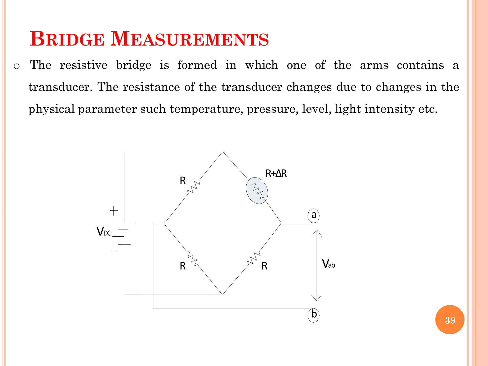
BRIDGE MEASUREMENTS
o The resistive bridge is formed in which one of the arms contains a
transducer. The resistance of the transducer changes due to changes in the
physical parameter such temperature, pressure, level, light intensity etc.
R
VDC
R
R
R+ΔR
a
b
Vab
39
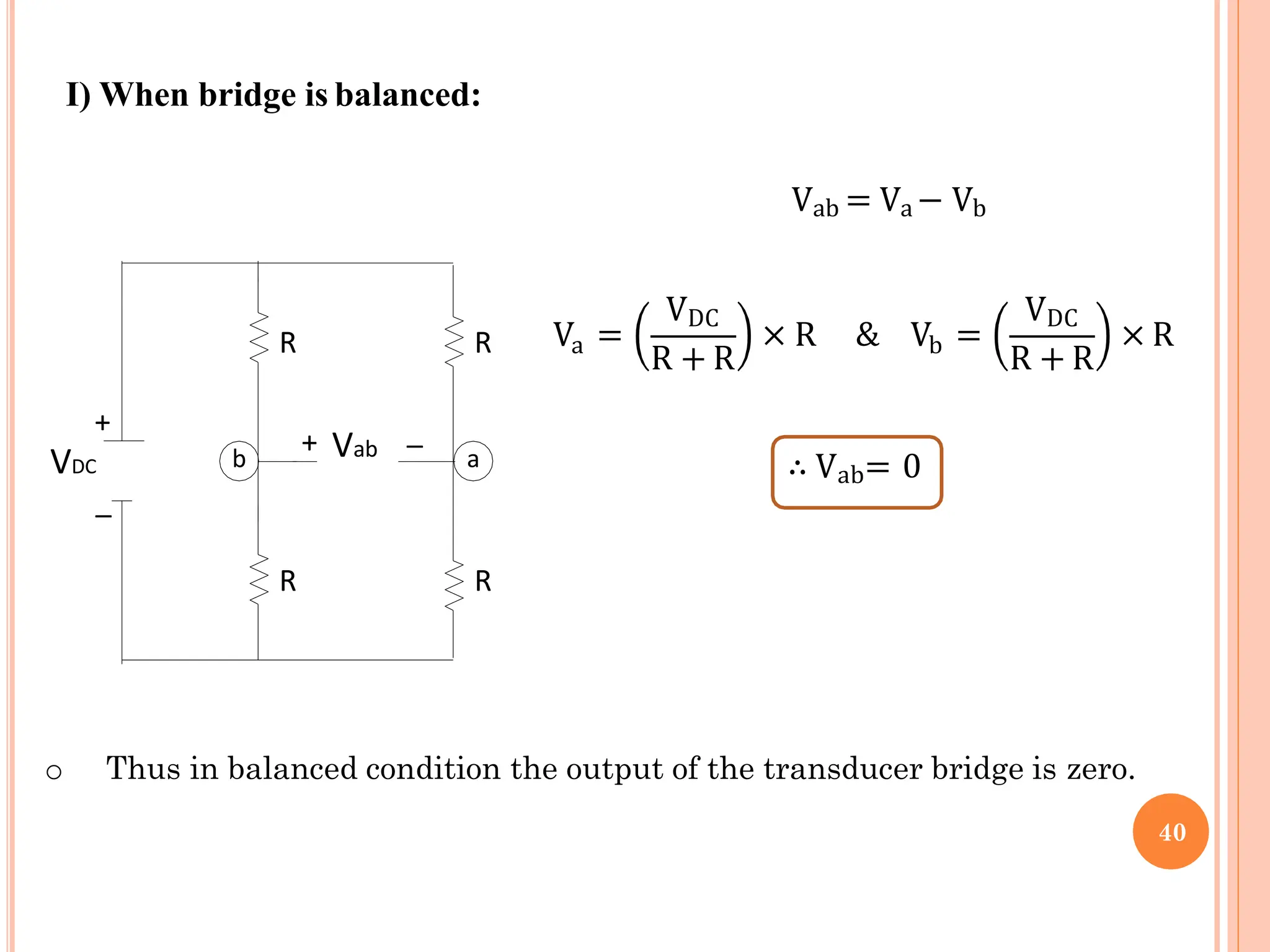
I) When bridge is balanced:
R
R
R
R
+
VDC
_
_
b a
+ Vab
Vab = Va − Vb
a
V =
VDC
R + R b
× R & V =
VDC
R + R
× R
∴ Vab= 0
o Thus in balanced condition the output of the transducer bridge is zero.
40
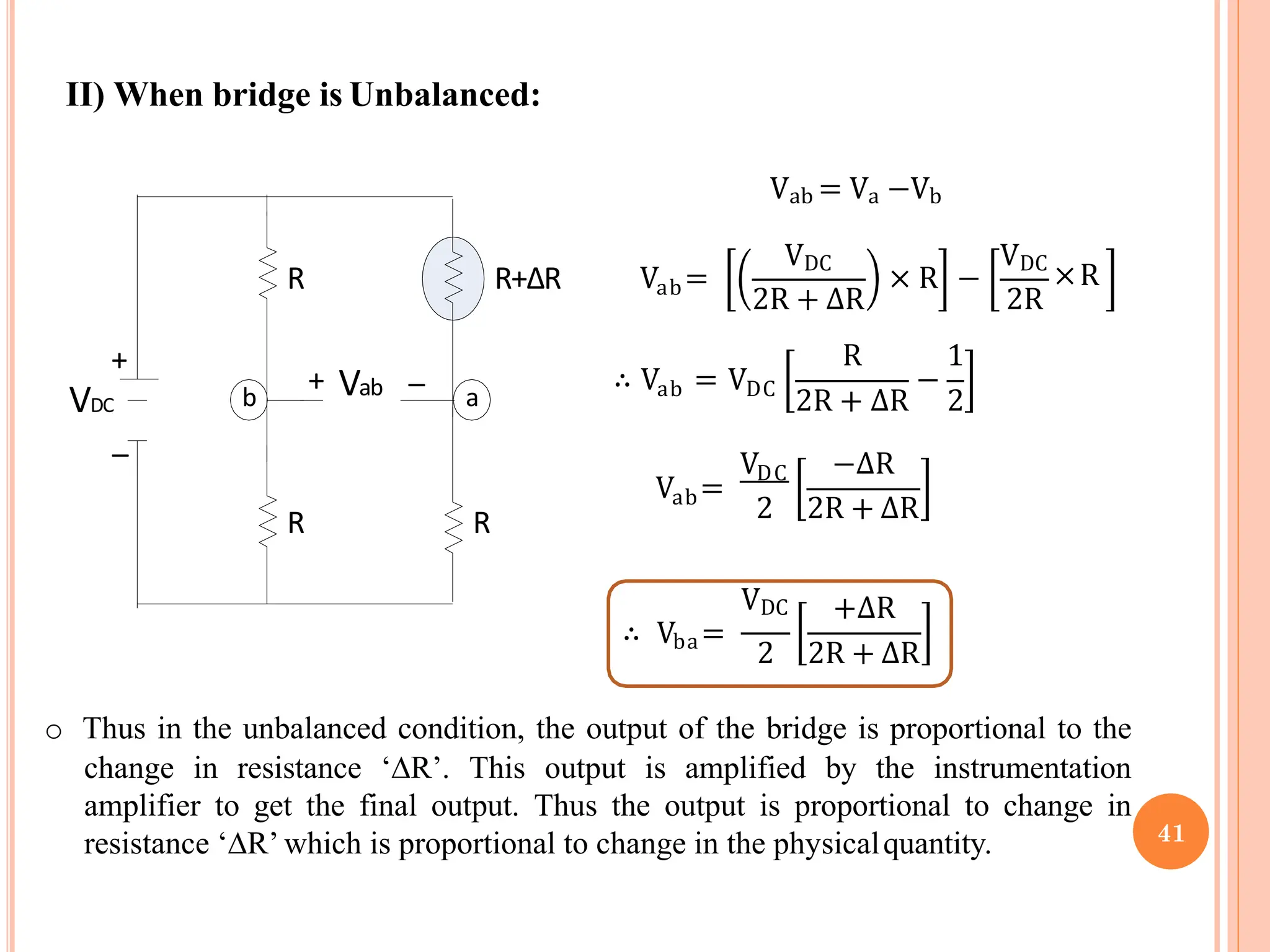
II) When bridge is Unbalanced:
R+ΔR
R
R
R
+
+
VDC
_
_
b a
Vab
Vab = Va −Vb
Vab=
VDC
2R + ∆R
× R −
2R
VDC
×R
ab
∴ V = VDC −
R 1
2R + ∆R 2
ab
V =
V −∆R
DC
2 2R + ∆R
ba
VDC
∴ V =
+∆R
2 2R + ∆R
o Thus in the unbalanced condition, the output of the bridge is proportional to the
change in resistance ‘∆R’. This output is amplified by the instrumentation
amplifier to get the final output. Thus the output is proportional to change in
resistance ‘∆R’ which is proportional to change in the physicalquantity. 41
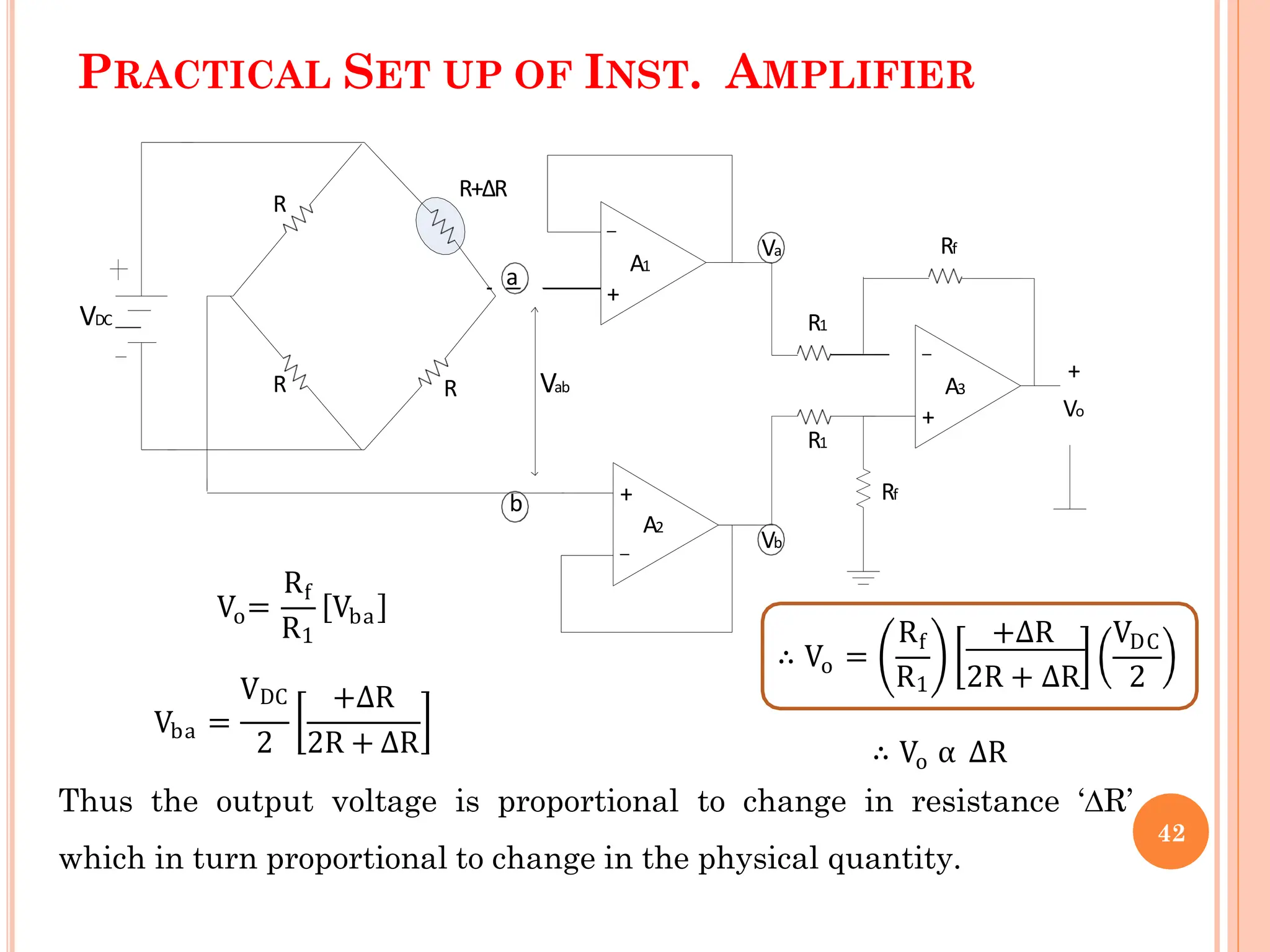
PRACTICAL SET UP OF INST. AMPLIFIER
R
VDC
R
R
R+ΔR
a
b
Vab
+
Vo
Rf
Rf
R1
R1
+
_
+
_
+
_
A1
A2
A3
Vb
Va
o
V =
Rf
R1
Vba
ba
VDC
V =
+∆R
2 2R + ∆R
o
∴ V =
R +∆R V
f DC
R1 2R + ∆R 2
o
∴ V α ∆R
Thus the output voltage is proportional to change in resistance ‘∆R’
which in turn proportional to change in the physical quantity.
42
APPLICATIONS OF INSTRUMENTATION AMPLIFIER
1. Analog Weighing Machine/Scale
2. Temperature Indicator:
3. Light Intensity Meter:
43
LECTURE # 09
 Basic Concept of Open Loop Comparator
 Input-Output Waveforms,
 Transfer Characteristics,
 Comparator Characteristics.
 Drawbacks of Open loop Comparator.
44
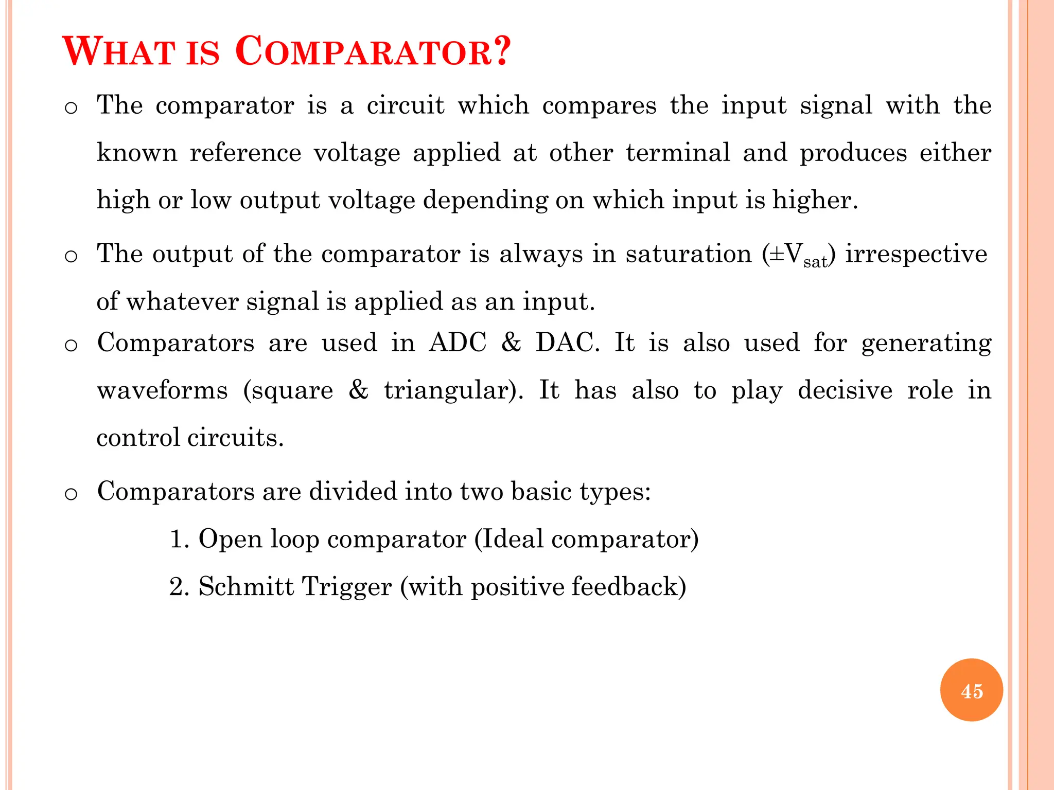
WHAT IS COMPARATOR?
o The comparator is a circuit which compares the input signal with the
known reference voltage applied at other terminal and produces either
high or low output voltage depending on which input is higher.
o The output of the comparator is always in saturation (±Vsat) irrespective
of whatever signal is applied as an input.
o Comparators are used in ADC & DAC. It is also used for generating
waveforms (square & triangular). It has also to play decisive role in
control circuits.
o Comparators are divided into two basic types:
1. Open loop comparator (Ideal comparator)
2. Schmitt Trigger (with positive feedback)
45
OPEN LOOP COMPARATOR
Operation :
1. If Vin > Vref, then Vo = +Vsat
2. If Vin < Vref, then Vo = -Vsat
+
_
Vo
+
Vin
_
Vref=0
+
_
V o
V in
NINV Comparator:
Vr e f = 0
+ V sat
-V sat
t
t
+ V sat
V o
V in
Vr e f = 0
-Vs a t
Vout = A (V+ - V-)
46
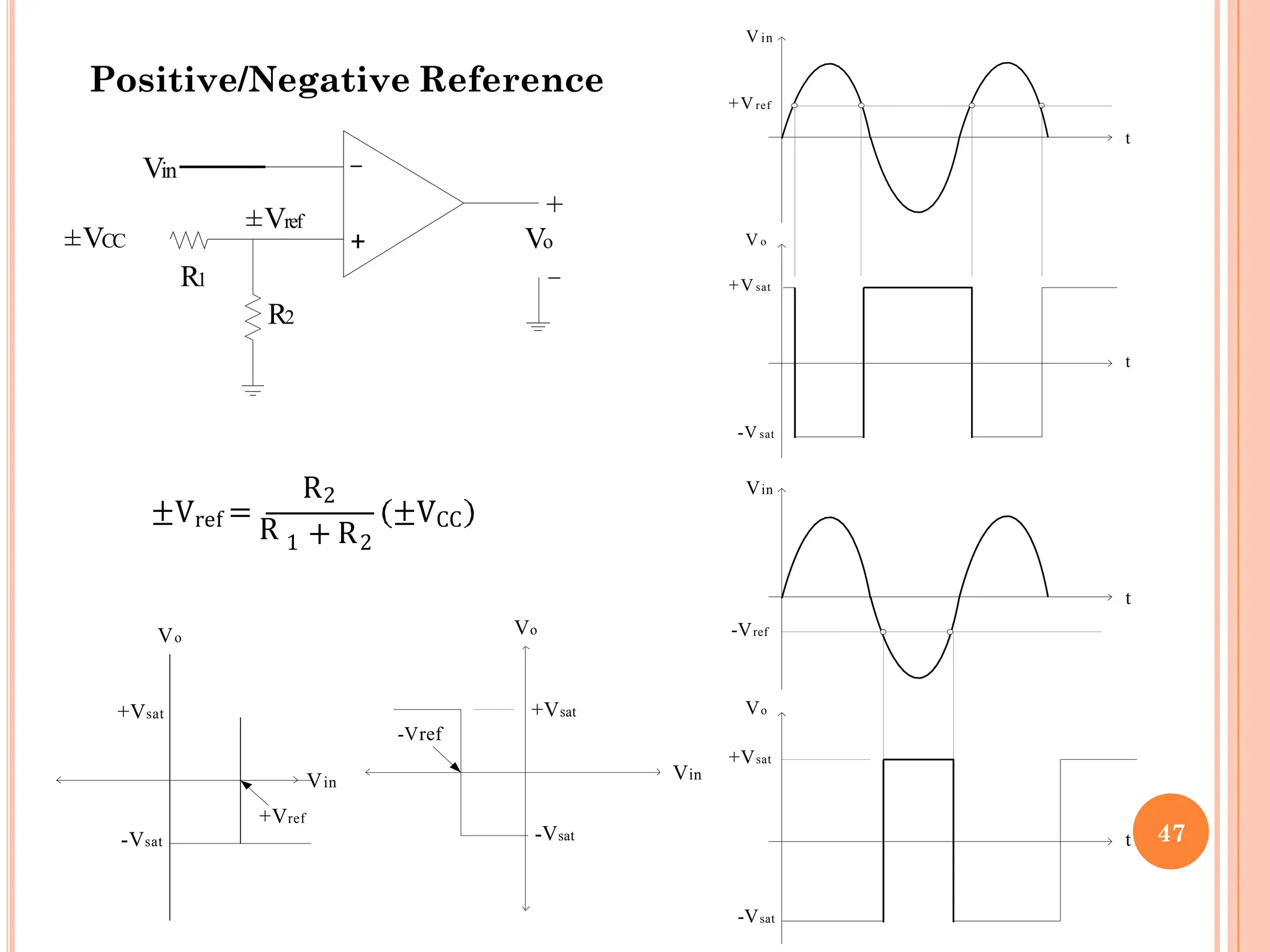
+
_
+
_
Vin
R1
R2
±VCC
±Vref
Vo
R2
±Vref =
R 1 + R2
±VCC
Vo
Vin
+Vref
+Vsat
-Vsat
t
t
Vo
Vin
-Vref
+Vsat
-Vsat
t
t
Vo
Vin
+Vsat
-Vsat
Vo
Vin
-Vref
+Vsat
-Vsat
+Vref
Positive/Negative Reference
47
COMPARATOR CHARACTERISTICS
1. Speed of operation:
The switching between the two output states should be as fast as
possible. Thus the output should respond the input changes quickly.
2. Accuracy:
It is the smallest amount of input difference voltage required to make
the output to change its state
3. Strobe function:
To enable/disable the device, certain comparators are having a strobe
terminal. When it is enable, output will respond to input. If it is
disabled, output will not respond to input signal.
4. Latch: some of the comparators are having latching facility. The
required output state is frozen in a latch flip flop. 48
5. Logic threshold:
It is the voltage level at the output of the comparator at
which the connected digital device changes its state. For
TTL it is approximately 1.2V and for CMOS it is 2.5V
6. Saturation Voltage:
The saturation voltage is the low output voltage level
with the input drive equal to or greater than the specified
value.
49
APPLICATIONS OF COMPARATOR
1. Duty Cycle Controller
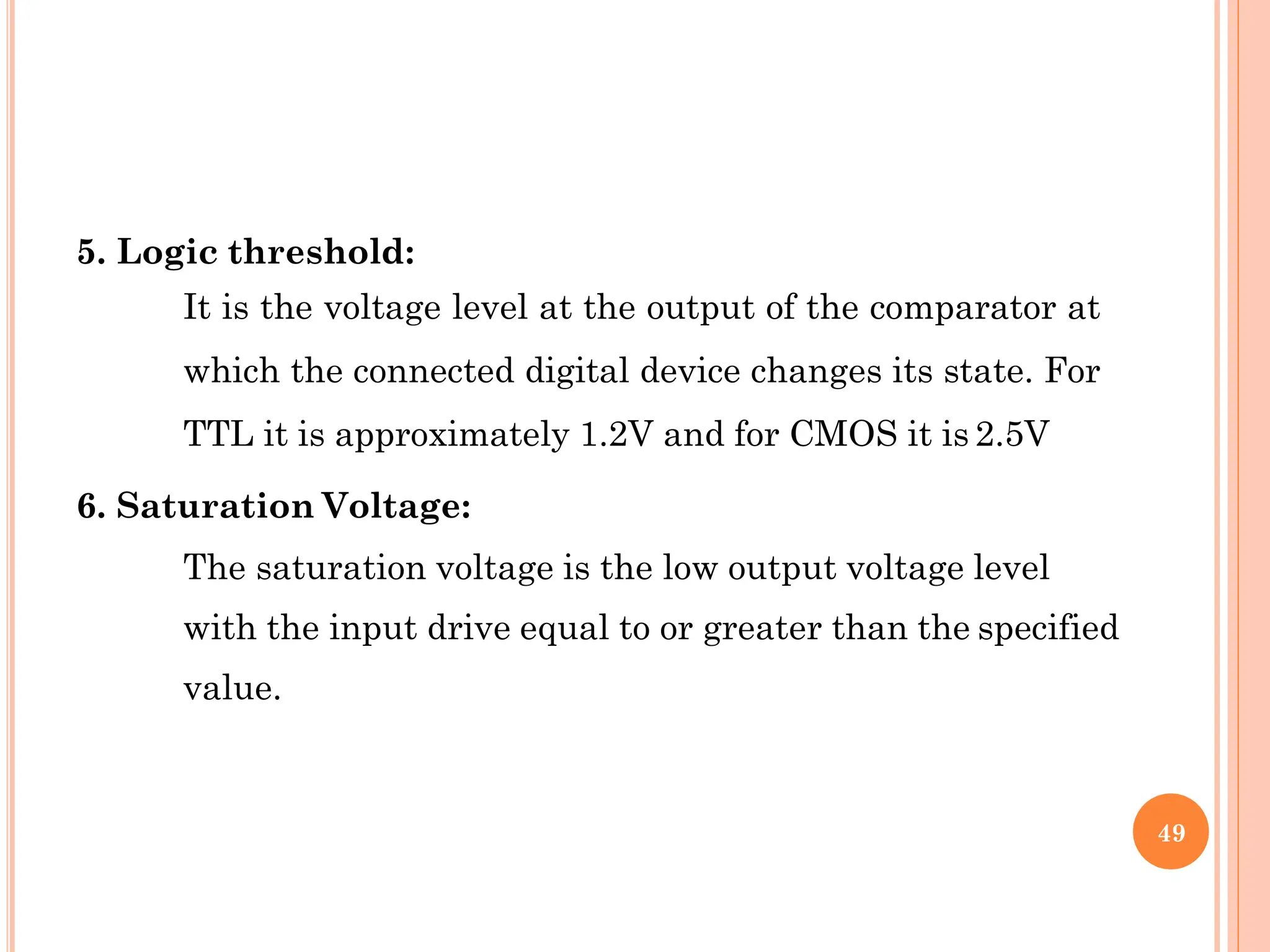
2. Window Comparator
3. Zero Crossing Detector
50
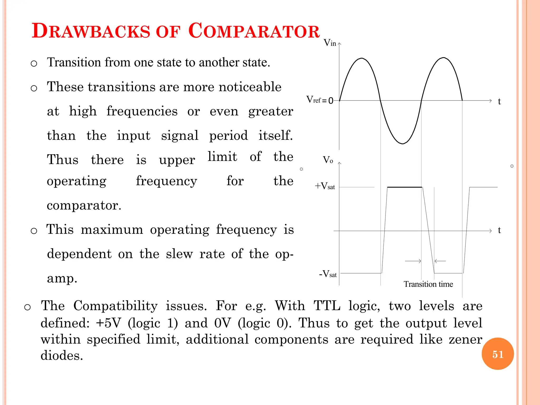
DRAWBACKS OF COMPARATOR
at high frequencies or even greater
than the input signal period itself.
Thus there is upper limit of the
for the
operating frequency
comparator.
o This maximum operating frequency is
dependent on the slew rate of the op-
amp.
Vo
Vin
o Transition from one state to another state.
o These transitions are more noticeable
Vref =0
+Vsat
-Vsat
t
t
Transition time
51
o The Compatibility issues. For e.g. With TTL logic, two levels are
defined: +5V (logic 1) and 0V (logic 0). Thus to get the output level
within specified limit, additional components are required like zener
diodes.
LECTURE # 10
 Inverting Symmetrical Schmitt Trigger.
 Derive threshold point equations.
 Input-Output Waveforms,
 Transfer Characteristics / Hysteresis Loop.
 Problems based on Inverting ST only.
52
INVERTING SCHMITT TRIGGER[SYMMETRICAL]
To avoid the false triggering apply a positive feedback and the circuit is
called as Schmitt trigger.
The triggering point VT is calculatedas
T
V =
R2
Vout
When Vin> VT ∴ Vo = −Vsat
When Vin< VT ∴ Vo = +Vsat
Vin
Vo
+Vsat
-Vsat
VUT
VLT
t
t
T
±V =
R1 +R2
R2
R1 +R2
±Vsat 53
+
_
Vin
Vo
+
_
R1
R2
±VT
HYSTERESIS LOOP
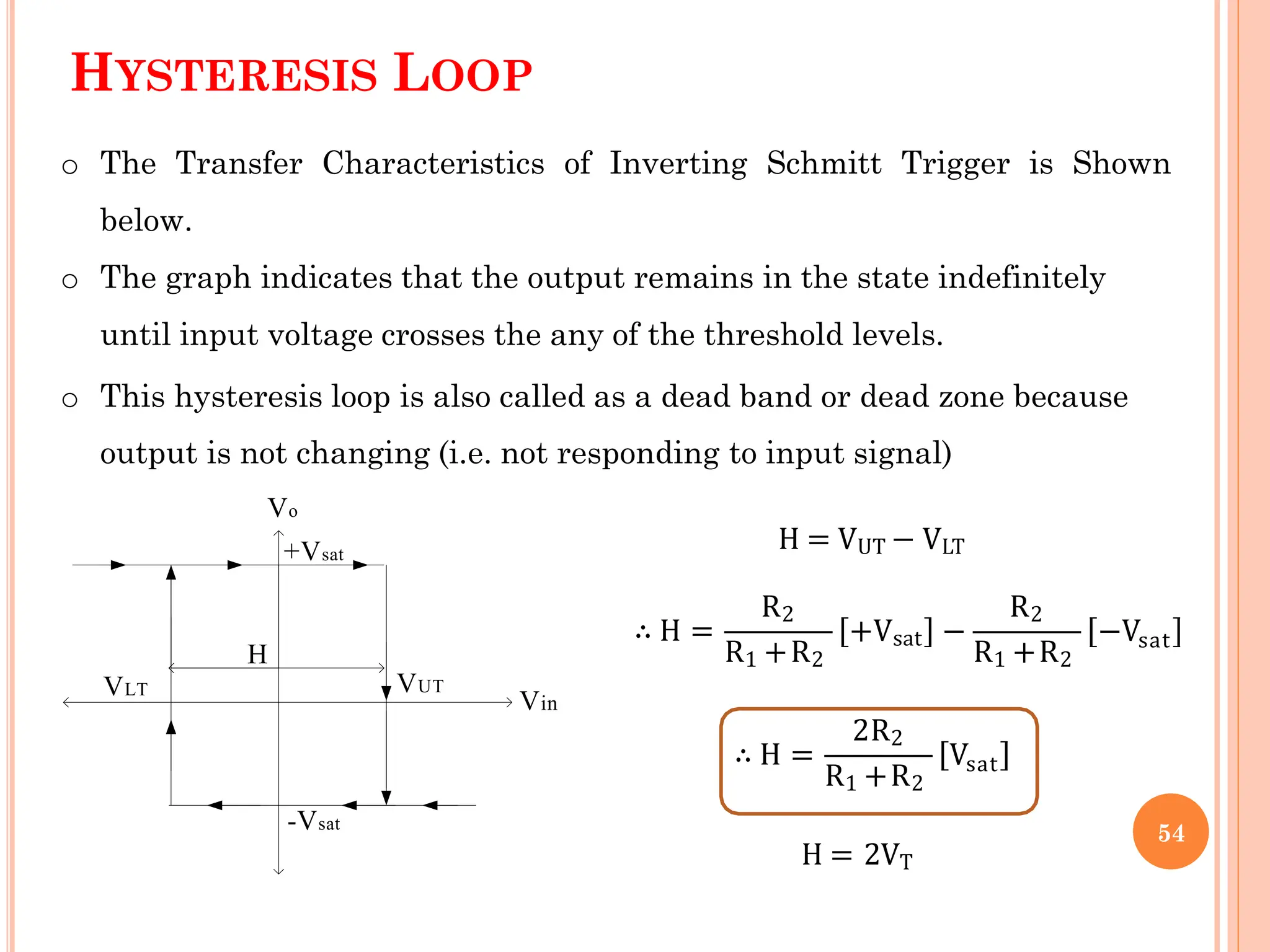
H = VUT − VLT
∴ H =
R2
R1 +R2
+Vsat −
R2
R1 +R2
−Vsat
∴ H =
2R2
R1 +R2
Vsat
H = 2VT
54
VLT VUT
+Vsat
-Vsat
o The Transfer Characteristics of Inverting Schmitt Trigger is Shown
below.
o The graph indicates that the output remains in the state indefinitely
until input voltage crosses the any of the threshold levels.
o This hysteresis loop is also called as a dead band or dead zone because
output is not changing (i.e. not responding to input signal)
Vo
Vin
H
LECTURE # 11
 Non-Inverting Symmetrical Schmitt Trigger.
 Derive threshold point equations.
 Inverting Asymmetrical Schmitt Trigger.
 Derive threshold point equations.
 Input-Output Waveforms,
 Transfer Characteristics / Hysteresis loop.
55
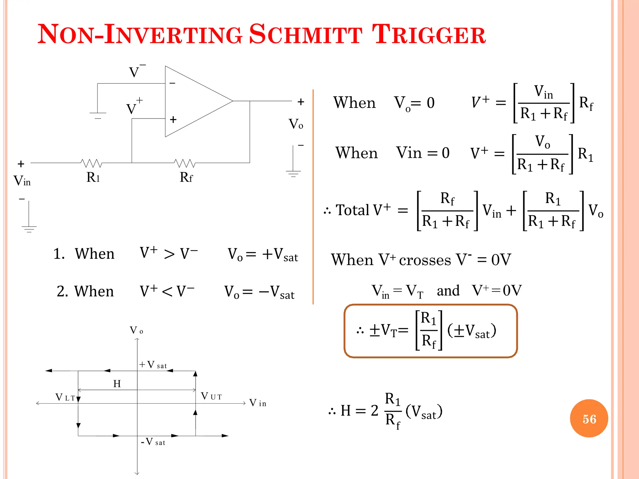
NON-INVERTING SCHMITT TRIGGER
+
_
Rf
R1
Vo
+
_
+
Vin
_
V
+
V
_
1. When V+
> V− Vo = +Vsat
2. When V+ < V− Vo = −Vsat
𝑉+ =
Vin
Rf
o
When V = 0
V+ =
R1 +Rf
Vo
R1 +Rf
R1
When Vin = 0
∴ Total V+ =
Rf
R1 +Rf
Vin +
R1
R1 +Rf
Vo
When V+ crosses V- = 0V
Vin = VT and V+ =0V
∴ ±VT=
R1
Rf
±Vsat
V L T V U T
+ V sat
-V sat
V o
V in
H
R1
∴ H = 2
Rf
Vsat 56
INVERTING SCHMITT TRIGGER[ASYMMETRICAL]
+
_
R1
Vin
+
_
_
Vo
+
_
V
VT
I R2
+
I
Vo = IR1 + IR2 +V
∴ I =
o
V − V
R + R
1 2
VT = IR2 + V
VT
R1 +R2
o
R R
R1 +R2
= 2
V + 1
V
Vin
Vo
+Vsat
-Vsat
VUT
VLT
t
t
VLT VUT
+Vsat
-Vsat
Vin
H
When
When
Vout = +Vsat
Vout = −Vsat
Vo
, VT = +ve
, VT= − ve
57
LECTURE # 12
 Waveform/Function Generator
 Circuit Diagram and Operation.
 Related Waveforms
 Derivation of output frequency.
 Problems based on it.
58
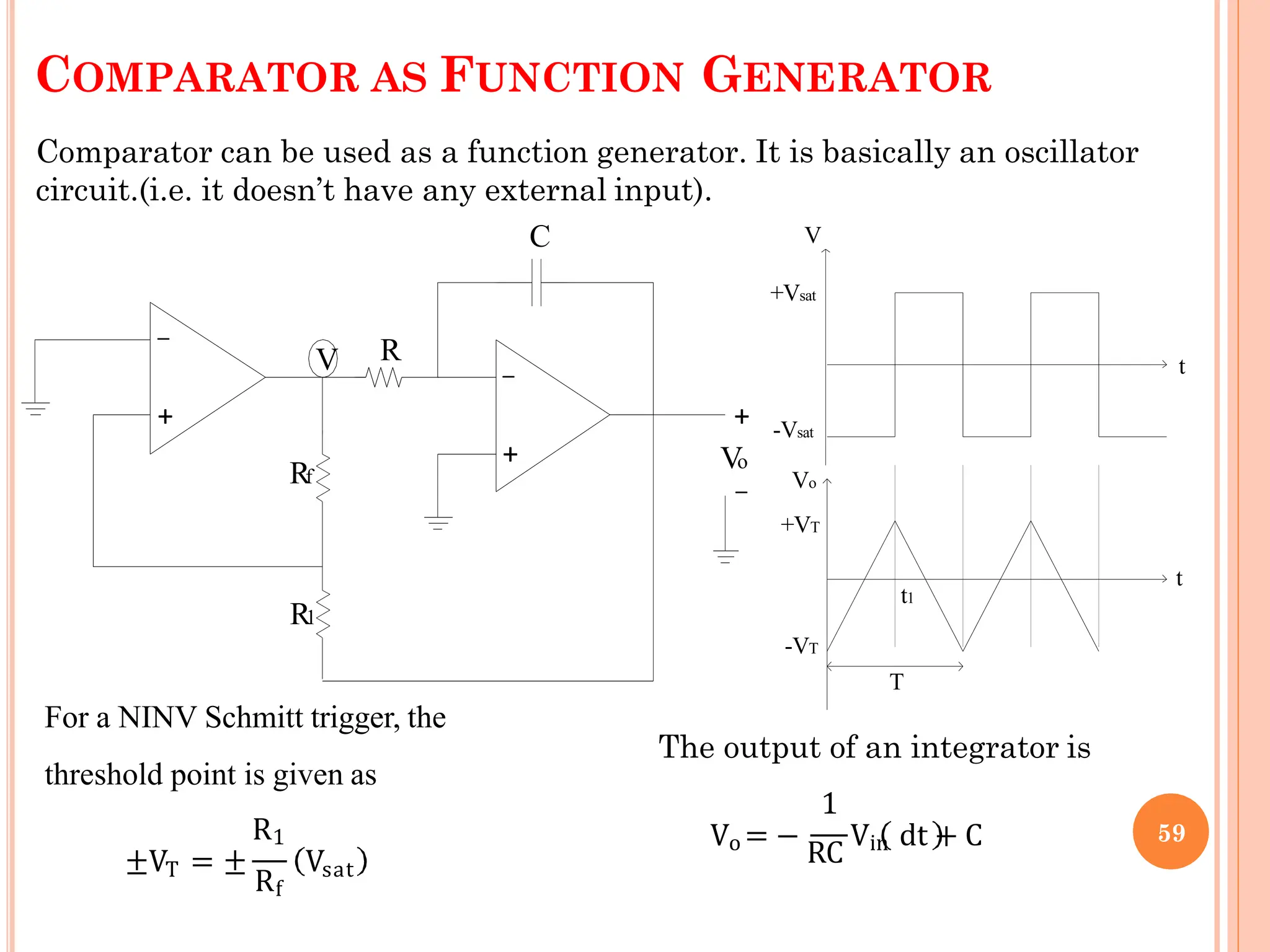
COMPARATOR AS FUNCTION GENERATOR
+
_
+
_
R1
Rf
R
C
Vo
+
_
V
-VT
+Vsat
-Vsat
Vo
+VT
V
T
t1
t
t
Comparator can be used as a function generator. It is basically an oscillator
circuit.(i.e. it doesn’t have any external input).
For a NINV Schmitt trigger, the
threshold point is given as
T
Rf
R1
±V = ± Vsat
1
Vo = −
RC
Vin dt + C
The output of an integrator is
59
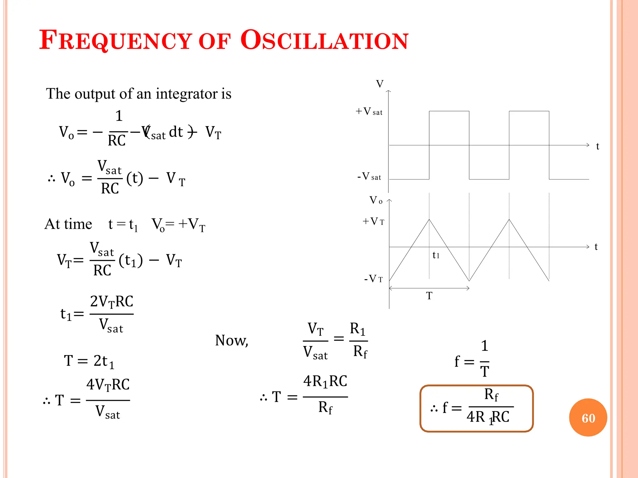
FREQUENCY OF OSCILLATION
The output of an integrator is
1
Vo = −
RC
−Vsat dt − VT
o
∴ V =
Vsat
RC
(t) − V T
At time t = t1 Vo= +VT
-VT
+Vsat
-Vsat
Vo
+VT
V
T
t1
t
t
T
V =
Vsat
RC
(t1) − VT
t1=
2VTRC
Vsat
T = 2t1
4VTRC
∴ T =
Vsat
Now,
Vsat
VT
=
R1
Rf
4R1RC
∴ T =
Rf
1
f =
T
Rf
1
∴ f =
4R RC 60
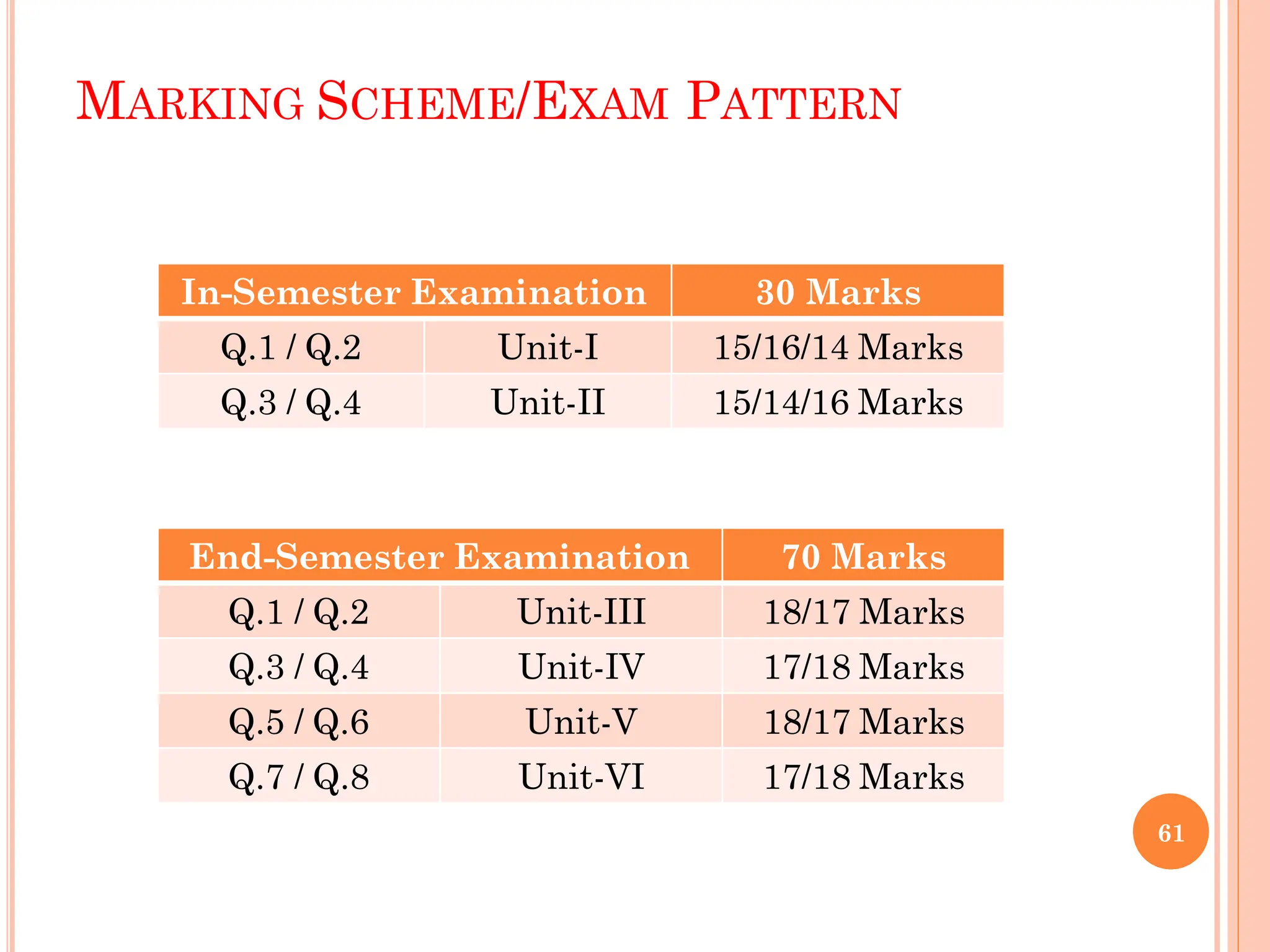
MARKING SCHEME/EXAM PATTERN
End-Semester Examination 70 Marks
Q.1 / Q.2 Unit-III 18/17 Marks
Q.3 / Q.4 Unit-IV 17/18 Marks
Q.5 / Q.6 Unit-V 18/17 Marks
Q.7 / Q.8 Unit-VI 17/18 Marks
In-Semester Examination 30 Marks
Q.1 / Q.2 Unit-I 15/16/14 Marks
Q.3 / Q.4 Unit-II 15/14/16 Marks
61
Thank You..!!
62

UNIT-V_Op-Amp Applications_Final sppu university

  • 1.
  • 2.
    SYLLABUS CONTENTS…  Inverting& Non inverting amplifier  Voltage follower,  Summing amplifier,  Differential amplifier,  Practical integrator,  Practical differentiator,  Instrumentation amplifier,  Comparator,  Schmitt trigger,  Square & triangular wave generator,  Precision rectifiers. CO5: Design, Build and test Op-amp based analog signal processing and Conditioning circuits towards various real time applications. 2
  • 3.
    TEXT BOOK/ REFERENCEBOOK  T2: Ramakant A. Gaikwad, “Op Amps and Linear Integrated Circuits”, Pearson Education 2000. and Kanchana Circuits”, Tata Bhaskaran, “Linear McGraw Hill, India  R3: Salivahanan Integrated 2008 3
  • 4.
    4 TOPIC REFERENCES Inverting &Non inverting amplifier R3 : 201 - 203 Voltage follower R3 : 186 - 187 Summing amplifier R3 : 193 - 194 Difference amplifier R3 : 194 - 195 Practical integrator R3 : 203 - 205 Practical differentiator R3 : 209 - 214 Instrumentation amplifier R3 : 196 - 200 Comparator R3 : 231 - 235 Schmitt trigger R3 : 237 - 239 Square & triangular wave generator R3 : 332 - 334
  • 5.
    LECTURE # 01 Virtual Ground/ Virtual Short.  Inverting amplifier.  Non inverting amplifier.  Voltage follower. 5
  • 6.
    VIRTUAL SHORT &VIRTUAL GROUND : non-inverting input : inverting input V+ V- Vout : output AOL : Open loop gain Vout = AOL (V+ - V-)= AOL Vid Ideally, Open loop gain AOL = infinite id AOL VOut V = V+ − V− = = 0 ∴ V+= V− V+ and V- are virtually short & not physically. 6
  • 7.
    INVERTING AMPLIFIER + _ Vin Rf R1 Vo + _ _ + I Vin Vo II = = − R R 1 f o ∴ V = − Rf R1 Vin Vin Vo t t 180° Phase shift Important points: 1. The phase shift between input and output is 180.̊ 2. The voltage gain is dependent on the two resistances R1 and Rf. 3. The circuit is also called as scale changer. If the gain is 1 it is called as phase inverter. 7
  • 8.
    NON-INVERTING AMPLIFIER Vin Vo −Vin I = R = R 1 f ∴ Vo = Vin 1 + Rf R1 Important points: 1. The phase shift between input and output is 0̊ i.e. input and output are in phase. 2. The voltage gain is always greater than 1 3. The circuit is also called as scale changer. + _ Rf R1 Vo + _ _ + I I Vin Vin Vo t t 0° Phase shift 8
  • 9.
    VOLTAGE FOLLOWER + _ Vo + _ _ + Vin ∴ Vo=Vin The gain of the circuit is 1; hence it is also called as unity gain amplifier. It is also called as buffer amplifier or source follower. Vin Vo t t Advantages: without 1. High input impedance. 2. Low output impedance. 3. High bandwidth. 4. The output follows input phase shift. 9
  • 10.
    LECTURE # 02 Summing Amplifier [2 Input] Inverting & Noninverting Type  Difference Amplifier [ Subtractor] 10
  • 11.
    ADDER/SUMMING AMPLIFIER Inverting adder: + _ Rf R1 Vo + _ I V1 V2 R2 I1 I2 I= I1 + I2 R = 0 − Vo V1− 0 R f 1 + V2− 0 R2 1 Rf Rf 2 ∴ Vo = − R V1 + R V2 If R1 = R2 = R o R Rf ∴ V = − V1+ V2 If Rf = R ∴ Vo = − V1+ V2 If R = 2Rf o V1+ V2 ∴ V = − 2 …. . 𝐴𝑉𝐸𝑅𝐴𝐺𝐸𝑅 11
  • 12.
    SUBTRACTOR/DIFFERENCE AMPLIFIER + + _ Rf Rf R2 V1 V2 Vo R1 I1 I1 I2 I2 V V Thesubtraction of the two input voltages is possible with the help of subtractor. 2 V2 − V V − 0 I = R = R 2 f ∴ V = V2 Rf R2 + Rf …. . (1) I1 = V1− V R1 = V − Vo Rf Rf Vo = V R1 + Rf − V1 … . (2) R1 Vo Rf = V2 R2 + Rf R1Rf R1Rf Rf R1 + Rf − V1 R1 If R1 = R2 o ∴ V = Rf R1 V2− V1 If R1 = R2 = Rf ∴ Vo= V2− V1 12
  • 13.
    LECTURE # 03 Basic/Ideal Integrator-  Circuit Diagram, Output equation  Response to Step, Square and Sinewave inputs  Frequency Response.  Drawbacks of Ideal Integrator. 13
  • 14.
    IDEAL/BASIC INTEGRATOR  Acircuit in which output voltage waveform is the time integral of the input voltage waveform is called integrator or integrating amplifier. + _ Vin + _ + _ Vo C R I I I = Vin −0 R d = C dt 0 − V0 ∴ dVo = − 1 RC Vindt 1 ∴ Vo = − RC Vin dt 14
  • 15.
    RESPONSE TO DIFFERENTINPUTS t t V m ω 2 V m ω V i n V m - V m V o 1 Vo = − RC Vin dt 1 Vo= − RC Vmsinωt dt o V V = − m ω – cosωt 1 Vo= − RC Vin dt 1 Vo= − RC V dt Vo = − V dt o V = − RC V RC t 15
  • 16.
    FREQUENCY RESPONSE OFAN IDEAL INTEGRATOR + _ Vin + + _ _ Vo C R I I −jXc 1 A = = R j2πfCR The magnitude of gain A is 1 A = As frequency increases, 2πfRC gain starts decreasing linearly at the rate of -20dB/decade. At f = fb , gain of the op-amp becomes unity (=1) i.e. 0 dB. 1 2πfbRC A = = 1 1 ∴ fb= 2πRC Therefore the gain A is given as A = 1 f f b f(Hz) |A|indB 0 -20dB/dec fb 16
  • 17.
    DRAWBACKS OF ANIDEAL INTEGRATOR o Bandwidth is very small and used for only small range of input frequencies. o At low frequencies, the opamp goes into saturation due to open loop condition. o Due to all such limitations, an ideal integrator needs to be modified. This modified integrator is referred as practical integrator. f (Hz) 0 |A| in dB -20 dB/dec fb 17
  • 18.
    LECTURE # 04 Practical Integrator- Circuit Diagram  Frequency Response and related observations.  Design Considerations.  How the Problems in ideal integrator are overcome in practical integrator.  Design equations and Problems. 18
  • 19.
    PRACTICAL INTEGRATOR R Vin + _ Vo Rf C + _ _ + o Addresistor Rf in parallel with capacitor C. avoids op-amp going into open loop configuration at low frequencies. 19
  • 20.
    FREQUENCY RESPONSE OFPRACTICAL INTEGRATOR Rf ∥ Xc A = R A = 1 Rf × jωC f R + 1 jωC A = R Rf 1 + jRfωC R Rf A = 1 R 1 + j2πfRfC a Let f = 1 f 2πR C =≫ Break frequency or Corner frequency R Rf 1 ∴ A = 1 + j f fa Where f =≫ Operating frequency R Rf Vin + _ Vo C + _ _ + 20
  • 21.
    A = Rf R 1 1 + f fa 2 Consider the following cases: 1. When f = 0 , the gain A = Rf R −−−− −dc gain 2. When a 0 < 𝑓 < f , the gain A ≅ Rf R a 3. When f > f , the gain A ≪ Rf R a 4. When f = f , the gain A = Rf 1 R 2 A = 0.707 Rf R fa |A| in dB 0 -20 dB/dec fb f (Hz) Rf R -3 dB [DC gain] 20 log10 True integration is possible over the range fa < 𝑓 <fb For better integration fb ≥ 10fa 21
  • 22.
    Prob: Design apractical integrator using Op-Amp IC 741C to satisfy the following specifications. Assume Vcc = +15V. 1) 3-dB cut-off frequency = 1.5 kHz 2) DC gain = 10 Sketch the frequency response of the circuit. Sol: Rf Given: fa = 1.5 KHz , DC gain = R = 10 a f = 1 2πR C Let f C = 0.1µf ∴ 𝐑𝐟 = 𝟏. 𝟎𝟔𝟏𝐤Ω R Rf DC gain = = 10 DC gain = 20log 10 Rf R = 20dB b f = fb = 10fa =15kHz 1 2πRC ∴ 𝐑 = 𝟏𝟎𝟔. 𝟏𝟎 Ω 𝐑𝐎𝐌 = 𝐑 ∥ 𝐑𝐟 = 96.4545 Ω |A| in dB 0 -20 dB/dec Rf R -3 dB [DC gain] 20 log10 R Vin + _ Rf C + Vo _ _ + 22 fa fb f (Hz)
  • 23.
    LECTURE # 05 Basic/Ideal Differentiator-  Circuit Diagram, Output equation  Response to Step, Square and Sinewave inputs  Frequency Response.  Drawbacks of Ideal Differentiator. 23
  • 24.
    IDEAL/BASIC DIFFERENTIATOR o Exchangethe positions of ‘R’ and ‘C’in integrator to get differentiator circuit. o The circuit which produces the differentiation of the input voltage at its output is called differentiator + _ + _ C R Vin _ + Vo I I −Vo dVin I = = C R dt o dV ∴ V = −RC in dt 24
  • 25.
    RESPONSE TO DIFFERENTINPUTS t V o V in A -A Vin Vo t t o dVin V = −RC dt d Vo= −RC dt Vmsinωt d Vo = −Vm dt sinωt Vo = −ωVm cosωt RC = 1 25
  • 26.
    FREQUENCY RESPONSE OFAN IDEAL DIFFERENTIATOR + _ + _ C R Vin + Vo _ I I A = R −jXc A = R −j 1 2πfC A = j2πfRC A = 2πfRC Thus the gain A isdirectly proportional to frequency f. fa f(Hz) |A|indB 0 +20dB/dec a f = 1 2πRC ∴ A = f fa When f < fa, the gain A is less than 1( i.e.negative) When f = fa, then the gain is 1 (i.e. 0dB) 26
  • 27.
    DRAWBACKS OF ANIDEAL DIFFERENTIATOR o Unstable at high frequencies.[Op-Amp may go into saturation] o Much Sensitive to noise at high frequencies leading to mis- amplification of the signal.. The reactance of the capacitor Xc is givenas 1 Xc = 2πfC As frequency increases, Xc reduces i.e. Capacitor draws more current from input source. 27
  • 28.
    LECTURE # 06 Practical differentiator- Circuit Diagram  Frequency Response and related observations.  Design Considerations.  How the Problems in ideal differentiator are overcome in practical differentiator.  Design equations and Problems. 28
  • 29.
    PRACTICAL DIFFERENTIATOR + _ + V_o C o Athigh frequencies the gain of the ideal differentiator is very high. This high gain makes the circuit unstable. Thus to avoid this resistance Rc is added in series with capacitor C and a capacitor Cc is added in parallel with resistance R. Cc R Rc Vin + _ Practically R.Cc= Rc.C 29
  • 30.
    FREQUENCY RESPONSE OFPRACTICAL DIFFERENTIATOR R ∥ −jXCc A = R𝐶 −jXC + _ + V_o Cc R C Rc Vin + _ Practically R.Cc=Rc.C A = ∴ A = −RjXCc Rc − jXc R − jXCc j2π R f C c j2πRf C + 1 j2π R f C + 1 ∴ A = j2πRfC j2π R f C + 1 j2π R f Cc +1 1 1 fa = 2πRC fb = 2πRC c 1 c = 2πR C ∴ A = f fa 1 + f fb 2 fb fa 0 |A| indB frequency(Hz) Closedloopresponseof op-amp . 30
  • 31.
     Select RC,C, R and CC such that the response cuts the actual response of the closed loop configuration of op-amp  Within the frequency range fa to fb the response is highly linear and hence referred as true differentiation range. Thus fb should be selected as high as possible as fa. The selection of frequencies should be in the following way ∴ fa< fb < fc where fc =≫ unity gain bandwidth of op − amp  Design procedure for practical differentiator: 1. Select fa as the highest frequency of input signal. a 2. Assume C and calculate R from the equation f = 1 2πRC 3. Select fb ≥ 10fa and calculate RC and CC so that RC.C = R.CC 31
  • 32.
     Prob: Designa practical differentiator for the input signal having maximum frequency of operation 150 Hz. Sol: Choose fmax = fa = 150Hz a f = 1 2πRC Let C = 0.1µf ∴ 𝐑 = 𝟏𝟎. 𝟔𝟏𝟎 𝐤Ω b f = 1 c 2πR C ∴ 𝐑𝐜 = 1.061 𝐤Ω Rc × C = Cc × R ∴ 𝐂𝐜 = 10𝐧𝐟 𝐑𝐎𝐌 = 𝐑 ∥ 𝐑𝐜 = 289.37 Ω + _ + V_o C For proper differentiation fb = 10fa = 1.5 kHz CC R RC Vin + _ ROM Practically R.Cc = Rc.C 32
  • 33.
    LECTURE # 07 Introduction and Significance.  Characteristics of Good Inst. Amplifier  3 Op-Amp Instrumentation Amplifier  Derivation of Output Voltage.  Problems based on equation. 33
  • 34.
    WHAT IS INSTRUMENTATIONAMPLIFIER o To amplify the low level output signal of a transducer so that it can drive the indicator or display is a measure function of an instrumentation amplifier. o The instrumentation amplifier is used for precise low level signal amplification where low noise, low thermal drift and high input resistance are required. o Besides this low power consumption, high CMRR and high slew rate are desirable for superior performance. 34
  • 35.
    REQUIREMENTS OF TYPICAL INSTRUMENTATIONAMPLIFIER SYSTEM  Differential input arrangement.  Single ended output.  Adjustable gain.  High Input Resistance  High CMRR  High Slew Rate  Low Power Dissipation.  Low offset & thermal drift. 35
  • 36.
    3 OP-AMP INSTRUMENTATIONAMPLIFIER + + + _ _ _ _ _ R R1 R1 R2 R2 Rf Rf + Vo _ + V1 + V2 V3 V4 A1 A3 A2 I I I (V4-V3) 36
  • 37.
    Let us assumevoltage V2 is more compared to V1 i.e. V2 > V1. Due to this current flow from V2 toV1 ∴ I = V2− V1 R 1 ∴ V4− V3= IR1 + IR + IR ∴ V4− V3= I 2R1 +R The voltage between the two points V4 and V3is ∴ V4− V3 = V2− V1 R 1 2R + R The op-amp A3 is the differential amplifier and its output is givenas o R2 Rf ∴ V = V − V 4 3 Rf ∴ Vo = R2 R 2R1 1 + V2− V1 Rf R2 2R1 1 + R V2− V1 => the gain of an instrumentation amplifier => the differential input to instrumentationamplifier + + + _ _ _ _ R R1 R1 R2 + R2 Rf Rf + Vo _ V1 _ + V2 V3 V4 A1 A3 A2 I I I (V4-V3) 37
  • 38.
    LECTURE # 08 Concept of Bridge type Measurements.  Balanced and Unbalanced Bridge and related outputs.  Typical Setup of Inst. Amplifier (Using Bridge and Diff. Amplifier)  Applications – Analog Weighing Machine, Temp. Detector, Light Intensity Meter 38
  • 39.
    BRIDGE MEASUREMENTS o Theresistive bridge is formed in which one of the arms contains a transducer. The resistance of the transducer changes due to changes in the physical parameter such temperature, pressure, level, light intensity etc. R VDC R R R+ΔR a b Vab 39
  • 40.
    I) When bridgeis balanced: R R R R + VDC _ _ b a + Vab Vab = Va − Vb a V = VDC R + R b × R & V = VDC R + R × R ∴ Vab= 0 o Thus in balanced condition the output of the transducer bridge is zero. 40
  • 41.
    II) When bridgeis Unbalanced: R+ΔR R R R + + VDC _ _ b a Vab Vab = Va −Vb Vab= VDC 2R + ∆R × R − 2R VDC ×R ab ∴ V = VDC − R 1 2R + ∆R 2 ab V = V −∆R DC 2 2R + ∆R ba VDC ∴ V = +∆R 2 2R + ∆R o Thus in the unbalanced condition, the output of the bridge is proportional to the change in resistance ‘∆R’. This output is amplified by the instrumentation amplifier to get the final output. Thus the output is proportional to change in resistance ‘∆R’ which is proportional to change in the physicalquantity. 41
  • 42.
    PRACTICAL SET UPOF INST. AMPLIFIER R VDC R R R+ΔR a b Vab + Vo Rf Rf R1 R1 + _ + _ + _ A1 A2 A3 Vb Va o V = Rf R1 Vba ba VDC V = +∆R 2 2R + ∆R o ∴ V = R +∆R V f DC R1 2R + ∆R 2 o ∴ V α ∆R Thus the output voltage is proportional to change in resistance ‘∆R’ which in turn proportional to change in the physical quantity. 42
  • 43.
    APPLICATIONS OF INSTRUMENTATIONAMPLIFIER 1. Analog Weighing Machine/Scale 2. Temperature Indicator: 3. Light Intensity Meter: 43
  • 44.
    LECTURE # 09 Basic Concept of Open Loop Comparator  Input-Output Waveforms,  Transfer Characteristics,  Comparator Characteristics.  Drawbacks of Open loop Comparator. 44
  • 45.
    WHAT IS COMPARATOR? oThe comparator is a circuit which compares the input signal with the known reference voltage applied at other terminal and produces either high or low output voltage depending on which input is higher. o The output of the comparator is always in saturation (±Vsat) irrespective of whatever signal is applied as an input. o Comparators are used in ADC & DAC. It is also used for generating waveforms (square & triangular). It has also to play decisive role in control circuits. o Comparators are divided into two basic types: 1. Open loop comparator (Ideal comparator) 2. Schmitt Trigger (with positive feedback) 45
  • 46.
    OPEN LOOP COMPARATOR Operation: 1. If Vin > Vref, then Vo = +Vsat 2. If Vin < Vref, then Vo = -Vsat + _ Vo + Vin _ Vref=0 + _ V o V in NINV Comparator: Vr e f = 0 + V sat -V sat t t + V sat V o V in Vr e f = 0 -Vs a t Vout = A (V+ - V-) 46
  • 47.
    + _ + _ Vin R1 R2 ±VCC ±Vref Vo R2 ±Vref = R 1+ R2 ±VCC Vo Vin +Vref +Vsat -Vsat t t Vo Vin -Vref +Vsat -Vsat t t Vo Vin +Vsat -Vsat Vo Vin -Vref +Vsat -Vsat +Vref Positive/Negative Reference 47
  • 48.
    COMPARATOR CHARACTERISTICS 1. Speedof operation: The switching between the two output states should be as fast as possible. Thus the output should respond the input changes quickly. 2. Accuracy: It is the smallest amount of input difference voltage required to make the output to change its state 3. Strobe function: To enable/disable the device, certain comparators are having a strobe terminal. When it is enable, output will respond to input. If it is disabled, output will not respond to input signal. 4. Latch: some of the comparators are having latching facility. The required output state is frozen in a latch flip flop. 48
  • 49.
    5. Logic threshold: Itis the voltage level at the output of the comparator at which the connected digital device changes its state. For TTL it is approximately 1.2V and for CMOS it is 2.5V 6. Saturation Voltage: The saturation voltage is the low output voltage level with the input drive equal to or greater than the specified value. 49
  • 50.
    APPLICATIONS OF COMPARATOR 1.Duty Cycle Controller 2. Window Comparator 3. Zero Crossing Detector 50
  • 51.
    DRAWBACKS OF COMPARATOR athigh frequencies or even greater than the input signal period itself. Thus there is upper limit of the for the operating frequency comparator. o This maximum operating frequency is dependent on the slew rate of the op- amp. Vo Vin o Transition from one state to another state. o These transitions are more noticeable Vref =0 +Vsat -Vsat t t Transition time 51 o The Compatibility issues. For e.g. With TTL logic, two levels are defined: +5V (logic 1) and 0V (logic 0). Thus to get the output level within specified limit, additional components are required like zener diodes.
  • 52.
    LECTURE # 10 Inverting Symmetrical Schmitt Trigger.  Derive threshold point equations.  Input-Output Waveforms,  Transfer Characteristics / Hysteresis Loop.  Problems based on Inverting ST only. 52
  • 53.
    INVERTING SCHMITT TRIGGER[SYMMETRICAL] Toavoid the false triggering apply a positive feedback and the circuit is called as Schmitt trigger. The triggering point VT is calculatedas T V = R2 Vout When Vin> VT ∴ Vo = −Vsat When Vin< VT ∴ Vo = +Vsat Vin Vo +Vsat -Vsat VUT VLT t t T ±V = R1 +R2 R2 R1 +R2 ±Vsat 53 + _ Vin Vo + _ R1 R2 ±VT
  • 54.
    HYSTERESIS LOOP H =VUT − VLT ∴ H = R2 R1 +R2 +Vsat − R2 R1 +R2 −Vsat ∴ H = 2R2 R1 +R2 Vsat H = 2VT 54 VLT VUT +Vsat -Vsat o The Transfer Characteristics of Inverting Schmitt Trigger is Shown below. o The graph indicates that the output remains in the state indefinitely until input voltage crosses the any of the threshold levels. o This hysteresis loop is also called as a dead band or dead zone because output is not changing (i.e. not responding to input signal) Vo Vin H
  • 55.
    LECTURE # 11 Non-Inverting Symmetrical Schmitt Trigger.  Derive threshold point equations.  Inverting Asymmetrical Schmitt Trigger.  Derive threshold point equations.  Input-Output Waveforms,  Transfer Characteristics / Hysteresis loop. 55
  • 56.
    NON-INVERTING SCHMITT TRIGGER + _ Rf R1 Vo + _ + Vin _ V + V _ 1.When V+ > V− Vo = +Vsat 2. When V+ < V− Vo = −Vsat 𝑉+ = Vin Rf o When V = 0 V+ = R1 +Rf Vo R1 +Rf R1 When Vin = 0 ∴ Total V+ = Rf R1 +Rf Vin + R1 R1 +Rf Vo When V+ crosses V- = 0V Vin = VT and V+ =0V ∴ ±VT= R1 Rf ±Vsat V L T V U T + V sat -V sat V o V in H R1 ∴ H = 2 Rf Vsat 56
  • 57.
    INVERTING SCHMITT TRIGGER[ASYMMETRICAL] + _ R1 Vin + _ _ Vo + _ V VT IR2 + I Vo = IR1 + IR2 +V ∴ I = o V − V R + R 1 2 VT = IR2 + V VT R1 +R2 o R R R1 +R2 = 2 V + 1 V Vin Vo +Vsat -Vsat VUT VLT t t VLT VUT +Vsat -Vsat Vin H When When Vout = +Vsat Vout = −Vsat Vo , VT = +ve , VT= − ve 57
  • 58.
    LECTURE # 12 Waveform/Function Generator  Circuit Diagram and Operation.  Related Waveforms  Derivation of output frequency.  Problems based on it. 58
  • 59.
    COMPARATOR AS FUNCTIONGENERATOR + _ + _ R1 Rf R C Vo + _ V -VT +Vsat -Vsat Vo +VT V T t1 t t Comparator can be used as a function generator. It is basically an oscillator circuit.(i.e. it doesn’t have any external input). For a NINV Schmitt trigger, the threshold point is given as T Rf R1 ±V = ± Vsat 1 Vo = − RC Vin dt + C The output of an integrator is 59
  • 60.
    FREQUENCY OF OSCILLATION Theoutput of an integrator is 1 Vo = − RC −Vsat dt − VT o ∴ V = Vsat RC (t) − V T At time t = t1 Vo= +VT -VT +Vsat -Vsat Vo +VT V T t1 t t T V = Vsat RC (t1) − VT t1= 2VTRC Vsat T = 2t1 4VTRC ∴ T = Vsat Now, Vsat VT = R1 Rf 4R1RC ∴ T = Rf 1 f = T Rf 1 ∴ f = 4R RC 60
  • 61.
    MARKING SCHEME/EXAM PATTERN End-SemesterExamination 70 Marks Q.1 / Q.2 Unit-III 18/17 Marks Q.3 / Q.4 Unit-IV 17/18 Marks Q.5 / Q.6 Unit-V 18/17 Marks Q.7 / Q.8 Unit-VI 17/18 Marks In-Semester Examination 30 Marks Q.1 / Q.2 Unit-I 15/16/14 Marks Q.3 / Q.4 Unit-II 15/14/16 Marks 61
  • 62.