PHOTONIC MATERIALS Rakesh Kumar Sinha
Photonics "Photonics"  comes from "photon" which is the smallest unit of light just as an electron is the smallest unit of electricity. "Photonics is the generation, process and manipulation of photon to achieve a certain function.
Why Do We Need Photonics instead of Electronics? An “All - Pervasive” Technology  1) Uninhibited light travels thousands of times faster than electrons in computer chips.   Optical computers will compute thousand of times faster than any electronic computer can ever achieve due to the physical limitation differences between light and electricity.  Can  pack more wavelengths  (that is information channels) into a optical fibre so that the  transmission bandwidth is increased  than conventional copper wires. Light  encounters  no electromagnetic interference  than that of electron in copper wires.
Photonic Crystals Principles and Applications
SO WHAT ARE PHOTONIC CRYSTALS ?   Photonic crystals are a new type of materials displaying unusual and attractive properties in the  interaction with light  Due to periodic modulation of the refractive index of a material, it is possible to  create tailored dispersion  relations and  stop bands of  light propagating through the material.
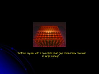
Photonic crystal with a complete band gap when index contrast is large enough
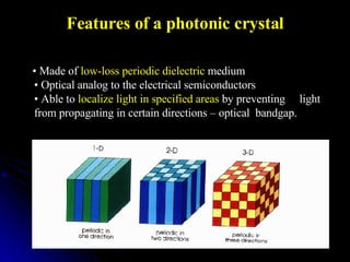
Features of a photonic crystal •  Made of  low-loss periodic dielectric  medium • Optical analog to the electrical semiconductors • Able to  localize light in specified areas  by preventing  light from propagating in certain directions – optical  bandgap.
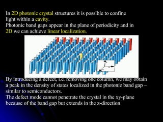
In  2D photonic crystal  structures it is possible to confine light within a  cavity . Photonic band gaps appear in the plane of periodicity and in 2D  we can achieve  linear localization . By introducing a defect, i.e. removing one column, we may obtain a peak in the density of states localized in the photonic band gap – similar to semiconductors. The defect mode cannot penetrate the crystal in the xy-plane because of the band gap but extends in the z-direction
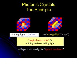
Photonic Crystals The Principle with photonic band gaps: “ optical insulators ” “ magical oven mitts”  for holding and controlling light can trap light in  cavities and  waveguides  (“wires”)
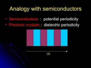
Photonic Crystals The Principle Periodic arrangement of ions  on a lattice gives rise to  energy band structure  in semiconductors ,which control motion of charge carriers through crystal. Similarly  ,in photonic crystals ,the  periodic arrangement of refractive index variation  ,controls how photons are able to move through crystal.
Analogy with semiconductors Semiconductors   :  potential periodicity Photonic crystals  :  dielectric periodicity 1D
Photonic band gap crystals -- a history   Idea of " photonic band gap structure " was first advanced in 1987 by  Eli Yablonovitch , now a professor at the University of California at Los Angeles.   In 1990, he built the  first photonic crystal , baseball-sized to channel microwaves useful in antennae applications
Photonic Band Gaps Photons with a certain range of wavelengths  do not have an energy state to occupy in a structure These photons are  forbidden  in the structure and cannot propagate Analogous  to  forbidden energy gaps  in semiconductors
Carefully engineered  line defects  could act as  waveguides  connecting photonic devices in all-optical microchips, and infiltration of the photonic material with suitable liquid crystals might produce photonic bandgap structures (and hence light-flow patterns) fully tunable by an externally applied voltage
Properties of Photonic Crystals
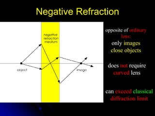
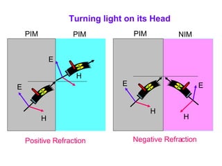
Negative Refraction opposite of   ordinary lens: only   images close objects does   not   require curved   lens can   exceed   classical diffraction limit
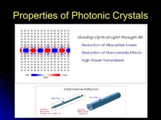
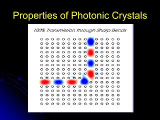
Properties of Photonic Crystals
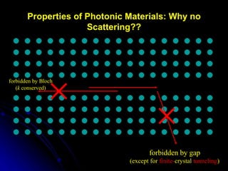
Properties of Photonic Materials: Why no Scattering?? forbidden by gap (except for   finite- crystal   tunneling ) forbidden by Bloch ( k  conserved)
Properties of Photonic Crystals
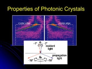
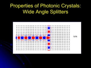
Properties of Photonic Crystals: Wide Angle Splitters
Applications Of Photonic Crystals Perfect mirror  :There are materials that reflect the  frequency range  of interest, with essentialy  no loss  at all. Such materials are widely available all the way from the ultraviolet regime to the microwave.   Nonlinear effects   : Using non-linear properties of materials for construction of photonic crystal lattices open new  possibilities for molding the flow of light. In this case the dielectric constant is additionally  depend on intensity of incident electromagnetic radiation and any non-linear optics phenomena can appeared.
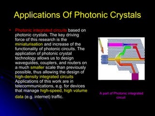
Applications Of Photonic Crystals Photonic integrated circuits   based on photonic crystals. The key driving force of this research is the  miniaturisation  and increase of the functionality of photonic circuits. The application of photonic crystal technology allows us to design waveguides, couplers, and routers on a much  smaller  scale than previously possible, thus allowing the design of  high-density integrated circuits  Applications of this work are in telecommunications, e.g. for devices that manage  high-speed, high volume data  (e.g. internet) traffic.   A part of Photonic integrated circuit
Applications Of Photonic Crystals Novel Semiconductor lasers and light emitters   : Efficient  light sources  (e.g. for lighting ,displays) and novel types of  optical sensors  ,e.g. for biomedical applications.
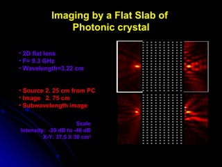
Imaging by a Flat Slab of  Photonic crystal Source 2. 25 cm from PC Image  2. 75 cm  Subwavelength image 2D flat lens F= 9.3 GHz Wavelength=3.22 cm Scale Intensity:  -20 dB to -40 dB X-Y: 37.5 X 30 cm 2
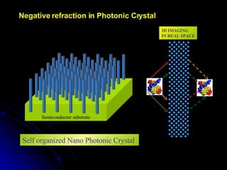
Self organized Nano Photonic Crystal  Negative refraction in Photonic Crystal 3D IMAGING IN REAL SPACE Semiconductor substrate
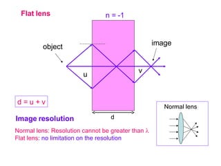
Flat lens n = -1 d d = u + v v u object image Normal lens: Resolution cannot be greater than   Flat lens : no limitation on the resolution Image resolution Normal lens
E H H E PIM PIM Turning light on its Head Positive Refraction PIM NIM E H E H Negative Refraction
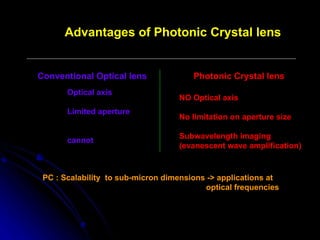
Conventional Optical lens   Photonic Crystal lens Advantages of Photonic Crystal lens Optical axis Limited aperture cannot NO Optical axis No limitation on aperture size Subwavelength imaging (evanescent wave amplification) PC : Scalability  to sub-micron dimensions -> applications at  optical frequencies
Applications Of Photonic Crystals Photonic transistor A transistor is a switch that is turned on and off by signals from other switches. They perform logic, store information and are the work horses of digital computing.  Photonic transistors  use light to perform the switching functions that are performed by electronic transistors in conventional computers.
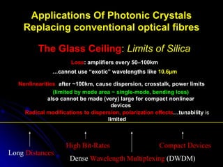
Applications Of Photonic Crystals Replacing conventional optical fibres The Glass Ceiling :  Limits of Silica Loss : amplifiers every 50–100km … cannot use “exotic” wavelengths like  10.6µm Nonlinearities :  after ~100km, cause dispersion, crosstalk, power limits (limited by mode area ~ single-mode, bending loss) also cannot be made (very) large for compact nonlinear devices Radical modifications to dispersion, polarization effects …tunability  is  limited Long  Distances High Bit-Rates Dense  Wavelength Multiplexing   (DWDM) Compact Devices
Future Applications Highly efficient photonic crystal lasers High resolution spectral filters Photonic crystal diodes and transistors High efficiency light bulbs Optical computers Telecommunication & computer networks Photonic clothes and candy bars??
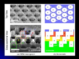
Fabrication Of Photonic Crystals An example of a two-dimensional photonic crystal. The distance between the 200 nm wide pillars is about 500 nm and the pillars are 1500 nm long.
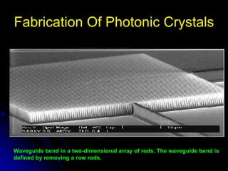
Fabrication Of Photonic Crystals Waveguide bend in a two-dimensional array of rods. The waveguide bend is defined by removing a row rods.
Fabrication Of Photonic Crystals Microfabrication :  By layer by layer lithography. Colloidal self-assembly.
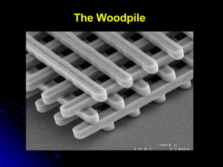
Fabrication Of Photonic Crystals The Biological Option  Layer-by-Layer Lithography •  Fabrication of   2d patterns in Si or GaAs is very advanced (think: Pentium IV, 50 million transistors) So, make 3d structure one layer at a time
 
The Woodpile
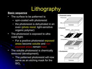
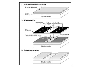
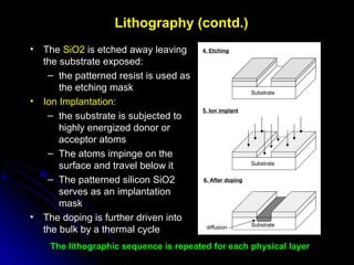
Lithography Basic sequence The surface to be patterned is: spin-coated with photoresist the photoresist is dehydrated in an oven ( photo resist : light-sensitive organic polymer) The photoresist is exposed to ultra violet light: For a positive photoresist  exposed areas  become  soluble  and  non exposed areas  remain  hard The soluble photoresist is chemically removed (development). The patterned photoresist will now serve as an etching mask for the SiO 2
 
The  SiO2  is etched away leaving the substrate exposed: the patterned resist is used as the etching mask Ion Implantation : the substrate is subjected to highly energized donor or acceptor atoms The atoms impinge on the surface and travel below it The patterned silicon SiO2 serves as an implantation mask The doping is further driven into the bulk by a thermal cycle Lithography (contd.) The lithographic sequence is repeated for each physical layer
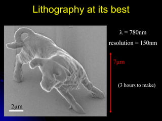
2µm Lithography at its best    = 780nm resolution = 150nm 7µm (3 hours to make)
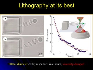
Lithography at its best 2µm ( 300nm diameter   coils, suspended in ethanol,   viscosity-damped )
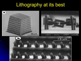
Lithography at its best
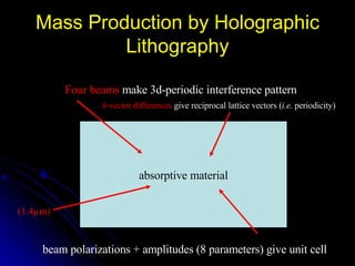
Mass Production by Holographic Lithography absorptive material Four beams   make 3d-periodic interference pattern (1.4µm) k -vector differences   give reciprocal lattice vectors ( i.e.  periodicity) beam polarizations + amplitudes (8 parameters) give unit cell
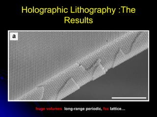
Holographic Lithography :The Results huge volumes ,  long-range periodic,   fcc   lattice…
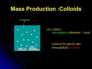
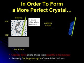
Mass Production :Colloids microspheres  (diameter < 1µm) silica   (SiO 2 ) sediment  by gravity into close-packed   fcc lattice ! (evaporate)
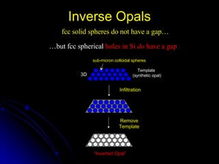
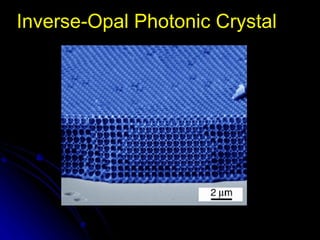
Inverse Opals fcc solid spheres do not have a gap…   … but fcc spherical   holes in Si  do  have a gap [ figs courtesy D. Norris, UMN ] Infiltration sub-micron colloidal spheres Template (synthetic opal) 3D Remove Template “ Inverted Opal”
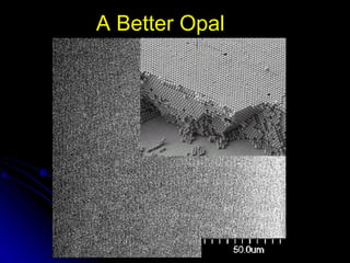
In Order To Form a More Perfect Crystal… meniscus silica 250nm Capillary forces   during drying cause   assembly in the meniscus Extremely   flat, large-area opals   of controllable thickness Heat Source 80C 65C 1 micron  silica spheres in ethanol evaporate  solvent
A Better Opal
Inverse-Opal Photonic Crystal
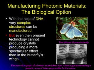
Manufacturing Photonic Materials: The Biological Option   With the help of  DNA  very  complex structures  can be  manufactured .   But  even then present technology cannot produce crystals producing a more spectacular effect than in the butterfly’s wings. The  Mitoura Grynea   butterfly   Electron micrograph of a broken scale taken from  mitoura grynea  revealing a periodic array of holes responsible for the colour
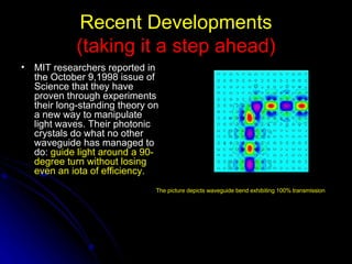
Recent Developments (taking it a step ahead) MIT researchers reported in the October 9,1998 issue of Science that they have proven through experiments their long-standing theory on a new way to manipulate light waves. Their photonic crystals do what no other waveguide has managed to do:  guide light around a 90-degree turn without losing even an iota of efficiency. The picture depicts waveguide bend exhibiting 100% transmission
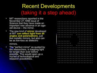
Recent Developments (taking it a step ahead) MIT researchers reported in the November 27,1998 issue of Science that they have made an important new advance in an age-old device -- the mirror.   The new kind of  mirror  developed at MIT  can reflect light from all angles and polarizations , just like metallic mirrors, but also can be as low-loss as dielectric mirrors.   The &quot;perfect mirror&quot; as quoted by the researchers, is trapping light for longer than ever before possible. This would open up a myriad of technological and research possibilities.
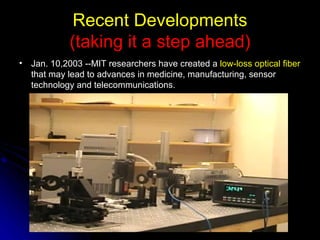
Recent Developments (taking it a step ahead) Jan. 10,2003 --MIT researchers have created a  low-loss optical fiber  that may lead to advances in medicine, manufacturing, sensor technology and telecommunications.
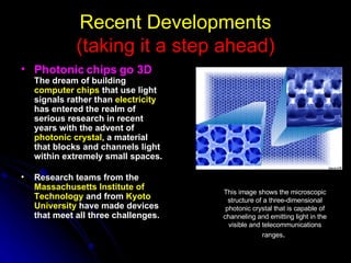
Recent Developments (taking it a step ahead) Photonic chips go 3D   The dream of building  computer chips  that use light signals rather than  electricity  has entered the realm of serious research in recent years with the advent of  photonic crystal , a material that blocks and channels light within extremely small spaces.   Research teams from the  Massachusetts Institute of Technology  and from  Kyoto University  have made devices that meet all three challenges.   This image shows the microscopic structure of a three-dimensional photonic crystal that is capable of channeling and emitting light in the visible and telecommunications ranges .
THANK  YOU !!!