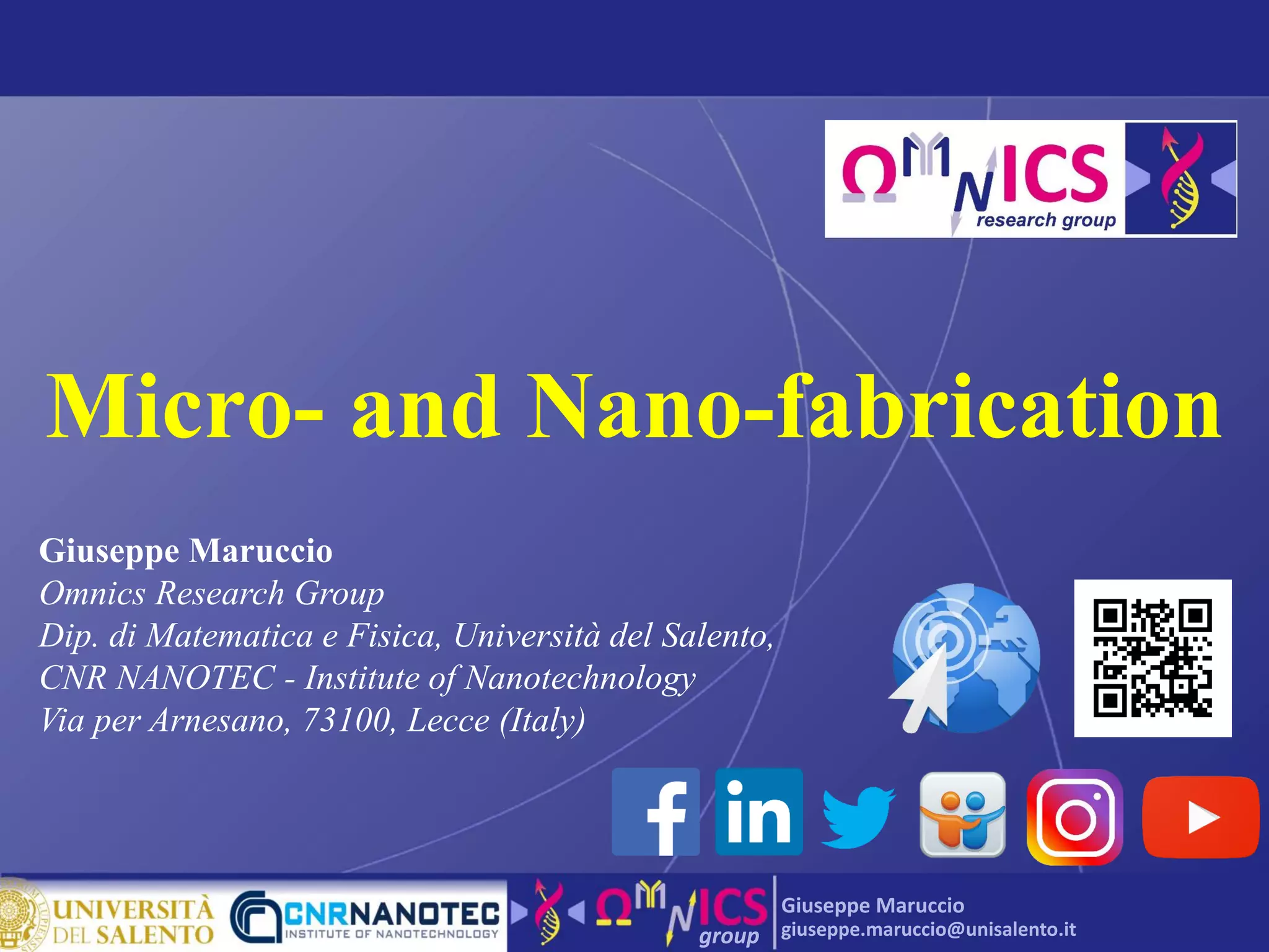


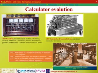
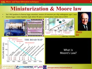

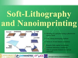
![giuseppe.maruccio@unisalento.it
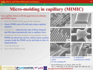
VIII. Micro- and Nano-fabrication techniques
└ Miniaturization & Tech.Nodes └ Semiconductor growth └ Lithography: λ, e, i, X, h/i, Altern., Soft
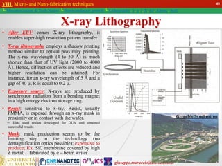
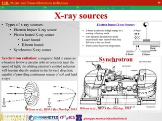
X-rays
Wilhelm Conrad
Roentgen (1845-1923)
x-rays are light (l = 10 nm to 0.01 nm)
Roentgen discovered an unknown ray in 1895 (X-ray) experimenting with
evacuated tubes that he would fill with specific gases and then pass electricity
through.
Roentgen found that despite shrouding the tube in black paper (as it let off a
glow similar to our incandescent bulbs) it somehow caused a barium
platinocyanide-coated screen to glow.
He won the first Nobel prize in physics in 1901
X-ray interactions
x-rays interact with matter through the excitation or ionization of
atomic electrons
absorption of high energy x-rays causes the creation of
photoelectrons (core shell holes) but does not lead directly to
resist modification [Cerrina, J Phys D, 2000]
relaxation is what leads to material modifications
• energy release of a higher lying electron via x-ray
fluorescence
• Auger effect – higher lying electron transfers energy to
another atomic electron, which is then ejected[eds. Suzuki, et
al., “Sub-Half-Micron Lithography for ULSIs”, 2000 ]
photoelectrons and auger electrons are responsible for
modification of resists
47](https://image.slidesharecdn.com/08micro-nano-fabrication-210217235022/85/08-Micro-Nano-Fabrication-47-320.jpg)

![giuseppe.maruccio@unisalento.it
VIII. Micro- and Nano-fabrication techniques
└ Miniaturization & Tech.Nodes └ Semiconductor growth └ Lithography: λ, e, i, X, h/i, Altern., Soft
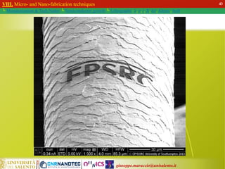
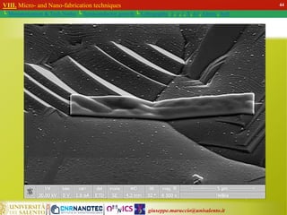
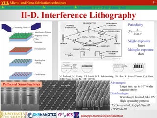
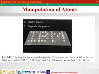
Nanofabrication. Scale bars: 2 m
[Kawata et al., Nature, 2001, 412, 697-698 ]
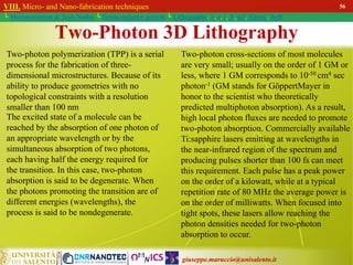
Two-Photon 3D Lithography
Satoshi Katawa and colleagues at Osaka University used two
laser beams to sculpt the micro-beast from resin, which
solidifies only where the lasers cross. The team refined this
'two-photon micropolymerization' to a resolution of 120
nanometres (120 billionths of a meter).
55](https://image.slidesharecdn.com/08micro-nano-fabrication-210217235022/85/08-Micro-Nano-Fabrication-55-320.jpg)


The document discusses micro- and nano-fabrication techniques, including various lithography methods and semiconductor growth processes. It emphasizes the evolution of technology in miniaturization, particularly Moore's Law, and the transition to advanced lithography methods such as extreme ultraviolet (EUV) lithography. Additionally, the author provides notes on the sources of presentation material and invites collaboration and feedback.


![Thin_Film_Technology_introduction[1]](https://cdn.slidesharecdn.com/ss_thumbnails/1b4496c8-2102-411b-8465-a3dd3f398327-150205034538-conversion-gate02-thumbnail.jpg?width=640&height=640&fit=bounds)


