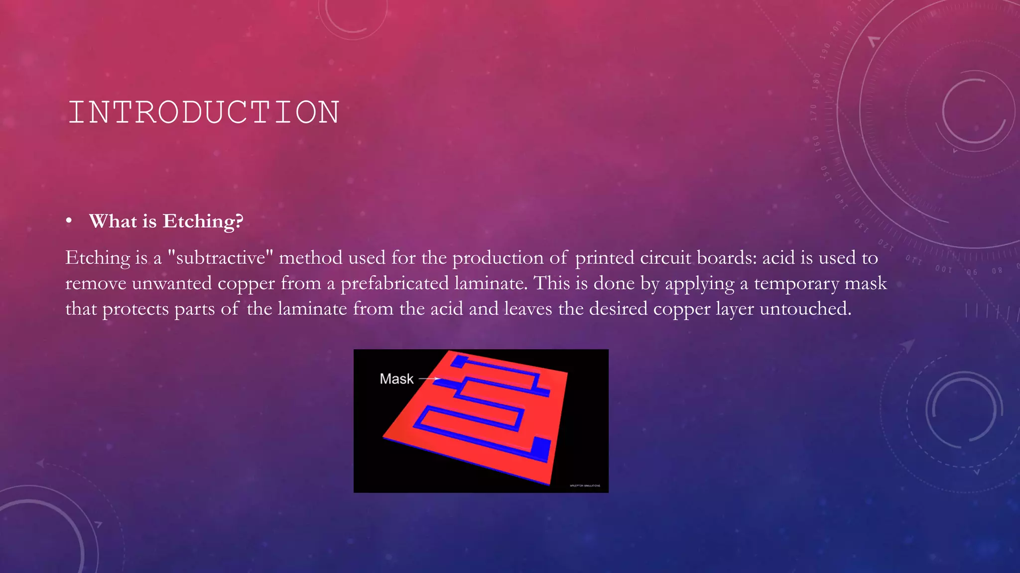
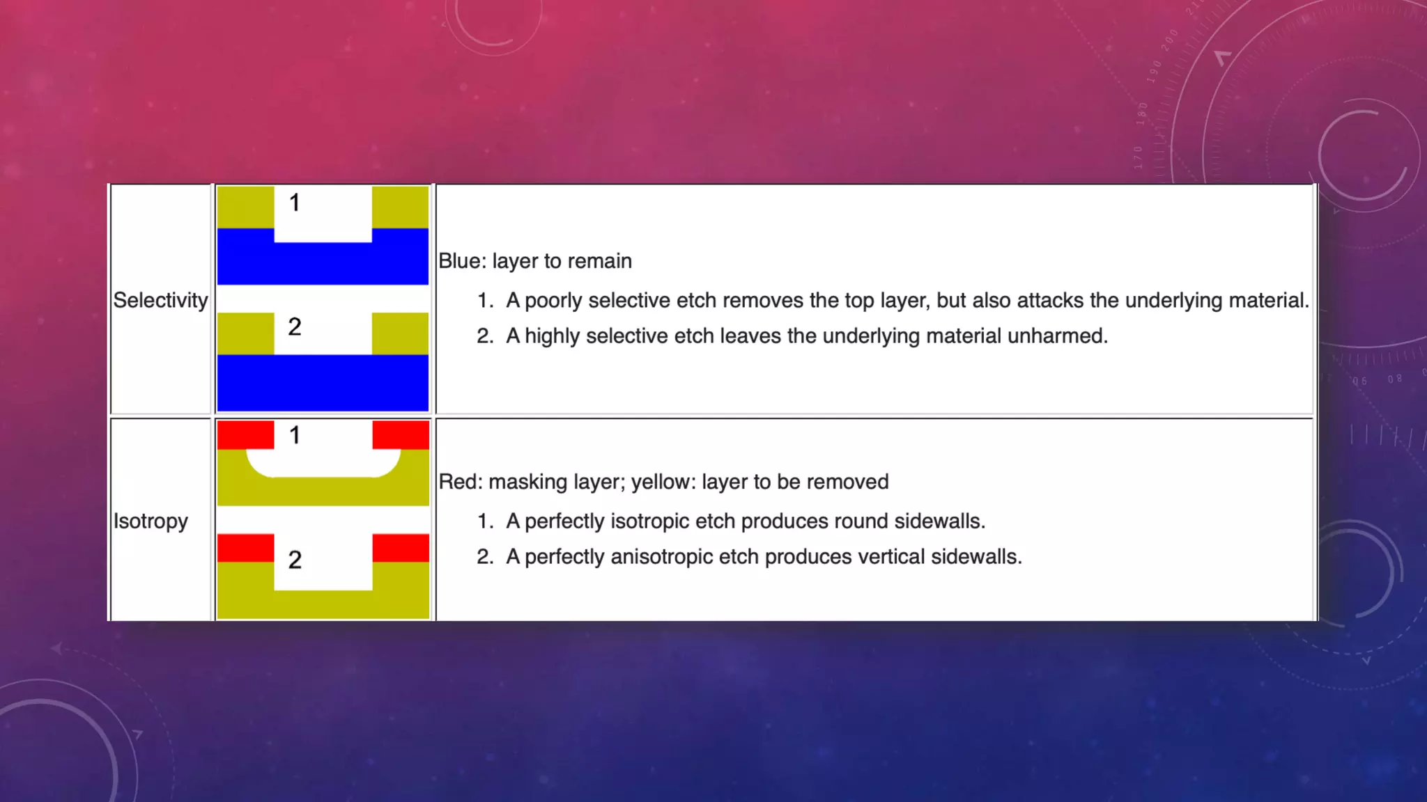
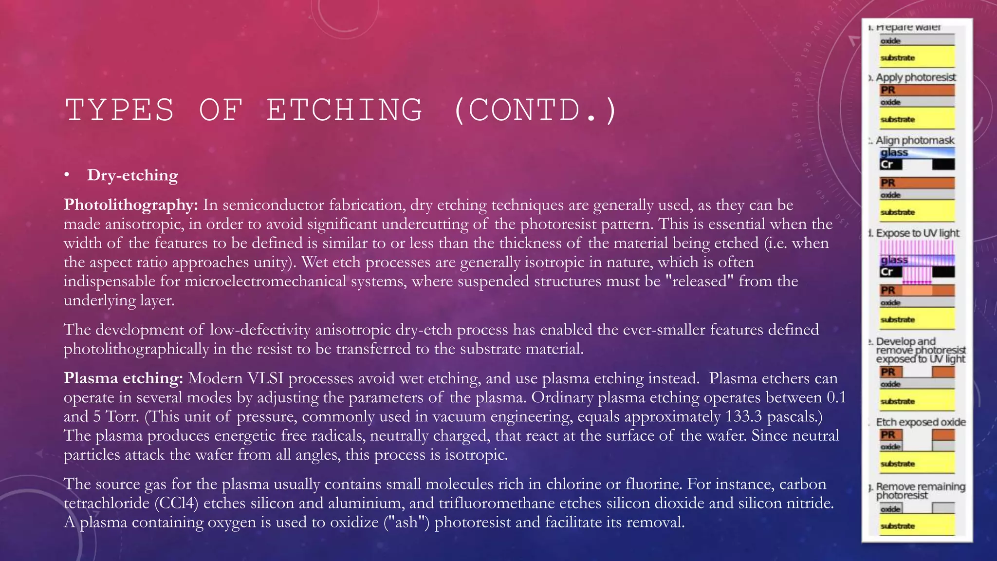
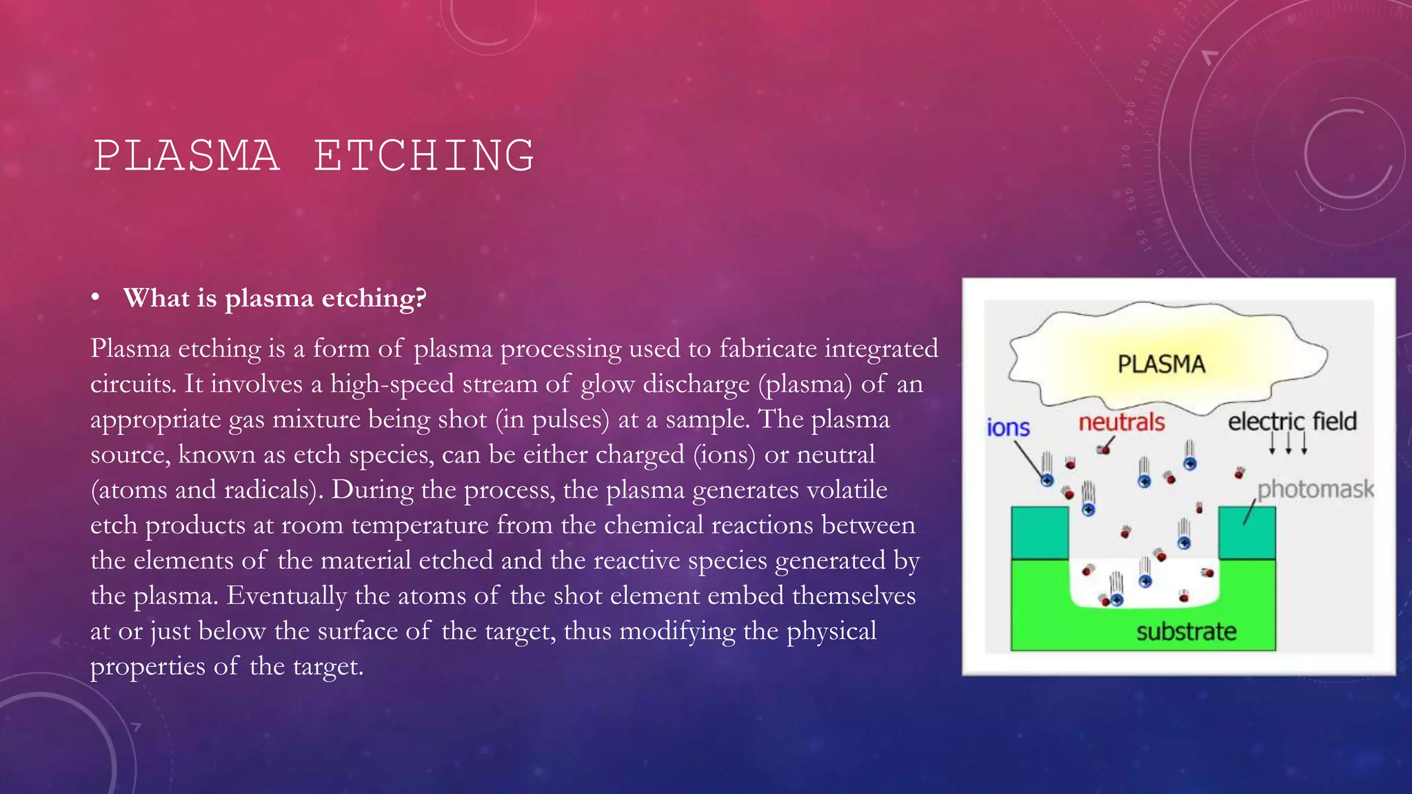
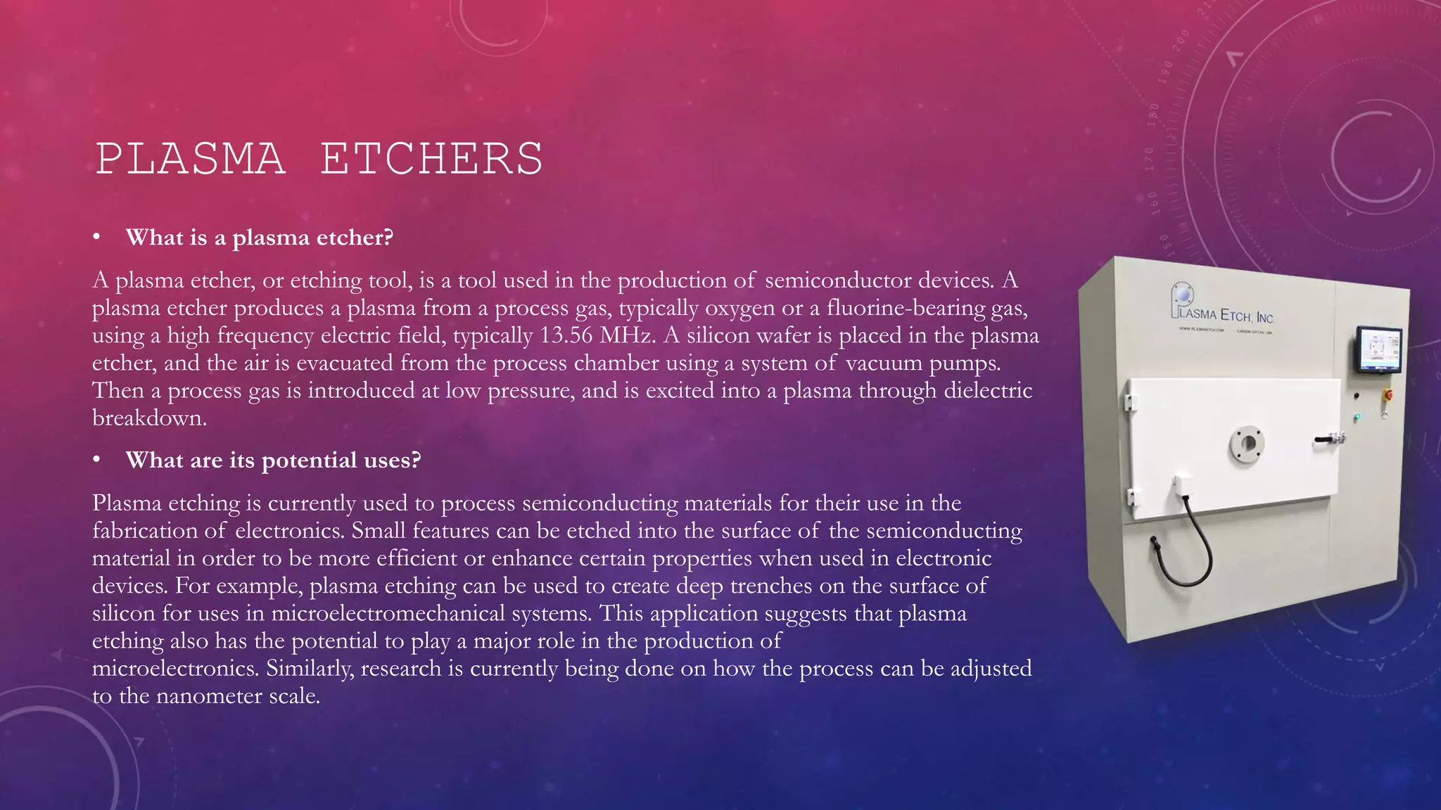
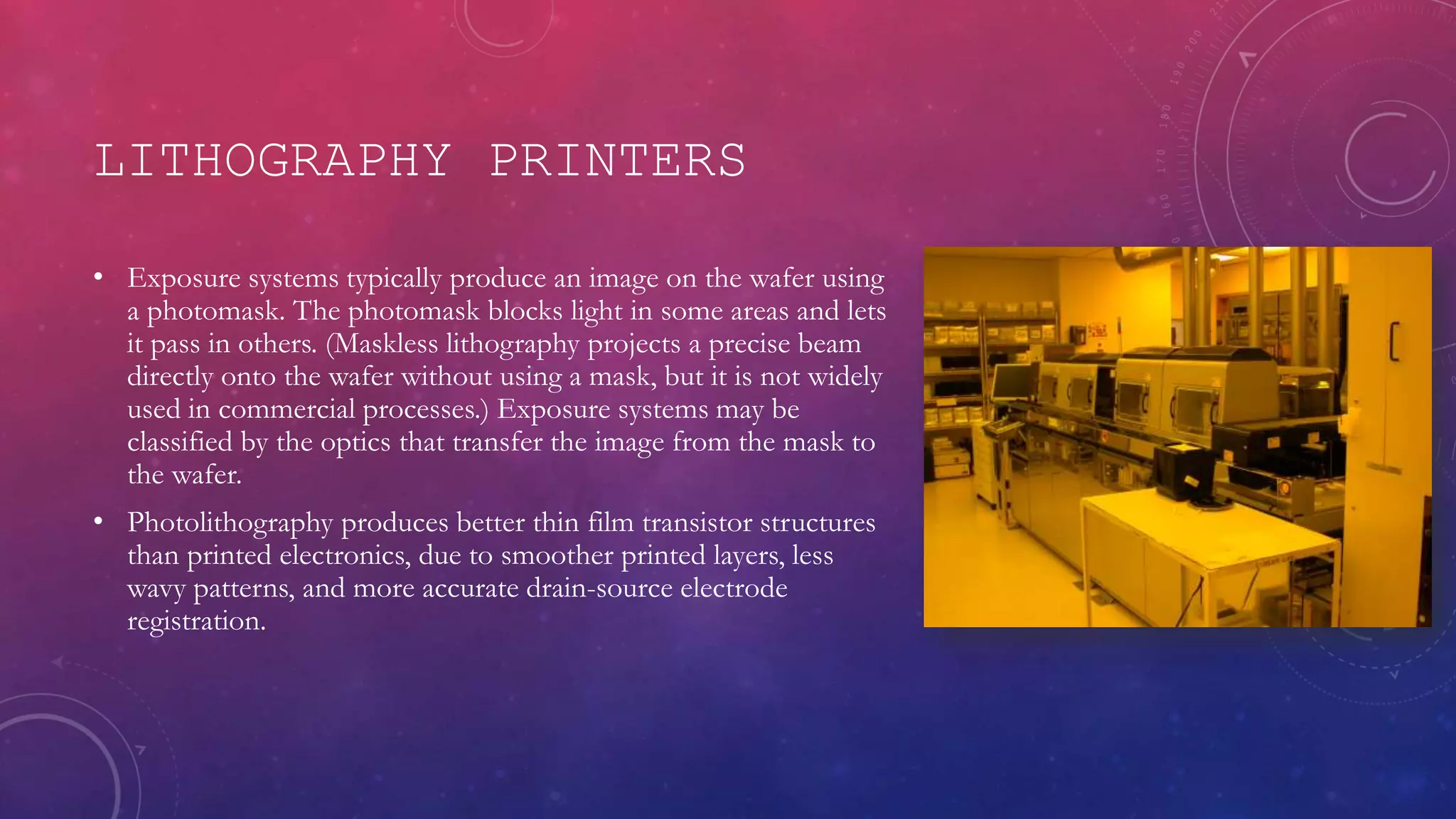
2. CONTENTS
• Introduction
• Figures of merit
• Basics of additive and subtractive processes
• Types of etching
• Types of etching (contd.)
• Plasma etching
• Plasma etchers
• Lithography printers
• References
3. INTRODUCTION
• What is Etching?
Etching is a "subtractive" method used for the production of printed circuit boards: acid is used to
remove unwanted copper from a prefabricated laminate. This is done by applying a temporary mask
that protects parts of the laminate from the acid and leaves the desired copper layer untouched.
5. FIGURES OF MERIT
• If the etch is intended to make a cavity in a material, the depth of the cavity may be controlled
approximately using the etching time and the known etch rate. More often, though, etching must
entirely remove the top layer of a multilayer structure, without damaging the underlying or
masking layers. The etching system's ability to do this depends on the ratio of etch rates in the
two materials (selectivity).
• Some etches undercut the masking layer and form cavities with sloping sidewalls. The distance of
undercutting is called bias. Etchants with large bias are called isotropic, because they erode the
substrate equally in all directions. Modern processes greatly prefer anisotropic etches, because
they produce sharp, well-controlled features.
6.
7. BASICS OF ADDITIVE AND SUBTRACTIVE
PROCESSES
• Subtractive methods remove copper from an entirely copper-coated board to leave only the desired copper pattern.
In additive methods the pattern is electroplated onto a bare substrate using a complex process. The advantage of
the additive method is that less material is needed and less waste is produced. In the full additive process the bare
laminate is covered with a photosensitive film which is imaged (exposed to light through a mask and then
developed which removes the unexposed film). The exposed areas are sensitized in a chemical bath, usually
containing palladium and similar to that used for through hole plating which makes the exposed area capable of
bonding metal ions. The laminate is then plated with copper in the sensitized areas. When the mask is stripped, the
PCB is finished.
• Semi-additive is the most common process: The unpatterned board has a thin layer of copper already on it. A
reverse mask is then applied. (Unlike a subtractive process mask, this mask exposes those parts of the substrate
that will eventually become the traces.) Additional copper is then plated onto the board in the unmasked areas;
copper may be plated to any desired weight. Tin-lead or other surface platings are then applied. The mask is
stripped away and a brief etching step removes the now-exposed bare original copper laminate from the board,
isolating the individual traces. Some single-sided boards which have plated-through holes are made in this way. The
(semi-)additive process is commonly used for multi-layer boards as it facilitates the plating-through of the holes to
produce conductive vias in the circuit board.
8. TYPES OF ETCHING
• Wet-etching
The first etching processes used liquid-phase ("wet") etchants. The wafer
can be immersed in a bath of etchant, which must be agitated to achieve
good process control. For instance, buffered hydrofluoric acid (BHF) is
used commonly to etch silicon dioxide over a silicon substrate.
Different specialised etchants can be used to characterise the surface
etched.
Wet etchants are usually isotropic, which leads to large bias when etching
thick films. They also require the disposal of large amounts of toxic waste.
For these reasons, they are seldom used in state-of-the-art processes.
However, the photographic developer used for photoresist resembles wet
etching.
9. TYPES OF ETCHING (CONTD.)
• Dry-etching
Photolithography: In semiconductor fabrication, dry etching techniques are generally used, as they can be
made anisotropic, in order to avoid significant undercutting of the photoresist pattern. This is essential when the
width of the features to be defined is similar to or less than the thickness of the material being etched (i.e. when
the aspect ratio approaches unity). Wet etch processes are generally isotropic in nature, which is often
indispensable for microelectromechanical systems, where suspended structures must be "released" from the
underlying layer.
The development of low-defectivity anisotropic dry-etch process has enabled the ever-smaller features defined
photolithographically in the resist to be transferred to the substrate material.
Plasma etching: Modern VLSI processes avoid wet etching, and use plasma etching instead. Plasma etchers can
operate in several modes by adjusting the parameters of the plasma. Ordinary plasma etching operates between 0.1
and 5 Torr. (This unit of pressure, commonly used in vacuum engineering, equals approximately 133.3 pascals.)
The plasma produces energetic free radicals, neutrally charged, that react at the surface of the wafer. Since neutral
particles attack the wafer from all angles, this process is isotropic.
The source gas for the plasma usually contains small molecules rich in chlorine or fluorine. For instance, carbon
tetrachloride (CCl4) etches silicon and aluminium, and trifluoromethane etches silicon dioxide and silicon nitride.
A plasma containing oxygen is used to oxidize ("ash") photoresist and facilitate its removal.
10. PLASMA ETCHING
• What is plasma etching?
Plasma etching is a form of plasma processing used to fabricate integrated
circuits. It involves a high-speed stream of glow discharge (plasma) of an
appropriate gas mixture being shot (in pulses) at a sample. The plasma
source, known as etch species, can be either charged (ions) or neutral
(atoms and radicals). During the process, the plasma generates volatile
etch products at room temperature from the chemical reactions between
the elements of the material etched and the reactive species generated by
the plasma. Eventually the atoms of the shot element embed themselves
at or just below the surface of the target, thus modifying the physical
properties of the target.
12. PLASMA ETCHERS
• What is a plasma etcher?
A plasma etcher, or etching tool, is a tool used in the production of semiconductor devices. A
plasma etcher produces a plasma from a process gas, typically oxygen or a fluorine-bearing gas,
using a high frequency electric field, typically 13.56 MHz. A silicon wafer is placed in the plasma
etcher, and the air is evacuated from the process chamber using a system of vacuum pumps.
Then a process gas is introduced at low pressure, and is excited into a plasma through dielectric
breakdown.
• What are its potential uses?
Plasma etching is currently used to process semiconducting materials for their use in the
fabrication of electronics. Small features can be etched into the surface of the semiconducting
material in order to be more efficient or enhance certain properties when used in electronic
devices. For example, plasma etching can be used to create deep trenches on the surface of
silicon for uses in microelectromechanical systems. This application suggests that plasma
etching also has the potential to play a major role in the production of
microelectronics. Similarly, research is currently being done on how the process can be adjusted
to the nanometer scale.
13. LITHOGRAPHY PRINTERS
• Exposure systems typically produce an image on the wafer using
a photomask. The photomask blocks light in some areas and lets
it pass in others. (Maskless lithography projects a precise beam
directly onto the wafer without using a mask, but it is not widely
used in commercial processes.) Exposure systems may be
classified by the optics that transfer the image from the mask to
the wafer.
• Photolithography produces better thin film transistor structures
than printed electronics, due to smoother printed layers, less
wavy patterns, and more accurate drain-source electrode
registration.
14. REFERENCES
• Books
Jaeger, Richard C. (2002). "Lithography". Introduction to Microelectronic Fabrication (2nd ed.).
Bunshah, Rointan F. (2001). Deposition Technologies for Films and Coatings.
Kohler, Michael (1999). Etching in Microsystem Technology.
• Websites
https://en.wikipedia.org/wiki/Plasma_etching
https://www.oxinst.com/products/etching-deposition-growth/processes-techniques/plasma-etch/Pages/plasma-
etch.aspx
http://www.lib.udel.edu/ud/spec/exhibits/color/lithogr.htm
https://en.wikipedia.org/wiki/Etching_(microfabrication)
http://www.dupont.com/products-and-services/electronic-electrical-materials/flexible-rigidflex-circuit-
materials/brands/pyralux-flexible-circuit.html
https://en.wikipedia.org/wiki/Printed_circuit_board