Download to read offline
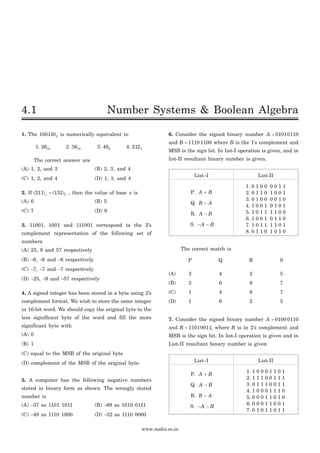
![Statement for Q.39–40:
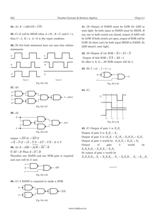
A Boolean function Z ABC= is to be implement
using NAND and NOR gate. Each gate has unit cost.
Only A, B and C are available.
39. If both gate are available then minimum cost is
(A) 2 units (B) 3 units
(C) 4 units (D) 6 units
40. If NAND gate are available then minimum cost is
(A) 2 units (B) 3 units
(C) 5 units (D) 6 units
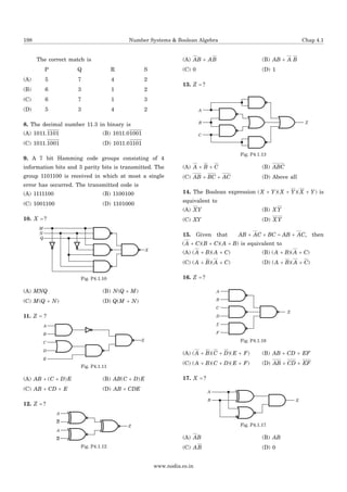
41. In fig. P4.1.41 the LED emits light when
(A) both switch are closed
(B) both switch are open
(C) only one switch is closed
(D) LED does not emit light irrespective of the
switch positions
42. If the input to the digital circuit shown in fig.
P.4.1.42 consisting of a cascade of 20 XOR gates is X,
then the output Y is equal to
(A) X (B) X
(C) 0 (D) 1
43. A Boolean function of two variables x and y is
defined as follows :
f f f( , ) ( , ) ( , )0 0 0 1 1 1 1= = = ; f ( , )1 0 0=
Assuming complements of x and y are not
available, a minimum cost solution for realizing f
using 2-input NOR gates and 2-input OR gates (each
having unit cost) would have a total cost of
(A) 1 units (B) 2 units
(C) 3 units (D) 4 units
44. The gates G1 and G2 in Fig. P.4.2.44 have
propagation delays of 10 ns and 20 ns respectively.
If the input Vi makes an abrupt change from logic
0 to 1 at t t= 0 then the output waveform Vo is
[t t1 0 10= + ns, t t2 1 10= + ns, t t3 2 10= + ns]
45. In the network of fig. P4.1.45 f can be written as
(A) X X X X X X X X X Xn n n0 1 3 5 2 4 5 1 1+ +- -.... ....
(B) X X X X X X X X X Xn n n0 1 3 5 2 3 4 1+ + -.... ....
(C) X X X X X X X X X X Xn n n n0 1 3 5 2 3 5 1.... ....+ + + -K
(D) X X X X X X X X X X X Xn n n n n0 1 3 5 1 2 3 5 1 2... ..- - -+ + + +K
*******
www.nodia.co.in
Chap 4.1 Number Systems & Boolean Algebra 201
t0 t1 t2 t3 t0 t1 t2 t3
t0 t1 t2 t3 t0 t1 t2 t3
(A)
(C)
(B)
(D)
VCC = 5 V
1 kW 1 kW 1 kW
1 kW
Fig. P4.1.41
1
X
Y
Fig. P4.1.42
1
Vi
0 Vi
G1
G2 Vo
to
Fig. P4.1.44
F
1
2
3
n
X1
X2
X3
Xn-1
Xn
X0
n-1
Fig. P4.1.45](https://image.slidesharecdn.com/numbersystems-180209133233/85/Number-systems-and-Boolean-Reduction-5-320.jpg)
![10. (D) X MNQ M NQ M NQ= + +
= +MQ M NQ = + = +Q M M N Q M N( ) ( )
11. (A) The logic circuit can be modified as shown in
fig. S. 4.1.11
Now Z AB C D E= + +( )
12. (D) You can see that input to last XNOR gate is
same. So output will be HIGH.
13. (D) Z A AB BC C= + + +( )
= + + + + +A A B B C C( ) = + +A B C
ABC A B C= + +
AB BC AC A B B C A C A B C+ + = + + + + + = + +
14. (C) ( )( )X Y X Y XY X Y+ + = +
( )( )( ) ( )( )X Y X Y X Y X Y XY X Y+ + + = + +
= + =XY XY XY
15. (B) Using duality
( )( )( ) ( )( )A B A C B C A B A C+ + + = + +
Thus (B) is correct option.
16. (B) Z AB CD EF= ( )( )( ) = + +AB CD EF
17. (A) X A B AB A B= + +( )( ) = + =( )( )AB A B AB AB
18. (B) Y A B C= Å ×( ) = + ×( )AB AC C
= + +( )AB AB C = + +A B AB C
19. (C) Z A A A BC ABC= + =( )
20. (A) Z AB B C ABC= + =( )
21. (A) Z A B BC AB BC ABC= + × = × =( ) ( )
22. (A) A A B A B C( )( )+ + +
= + + + = + + =( )( ) ( )AA AB A B C A A B C A
Therefore No gate is required to implement this
function.
23. (A)
A B C ( )A BC+ ( )( )A B A C+ +
0 0 0 0 0
0 0 1 0 0
0 1 0 0 0
0 1 1 1 1
1 0 0 1 1
1 0 1 1 1
1 1 0 1 1
1 1 1 1 1
Fig. S 4.1.23
24. (B) X ABC ABC ABC= + + = +BC ABC
25. (B) ( )( ) ( )( )A B B C AB BC ABC+ + = =
( )( ) ( ) ( )A B B C A B B C A B C+ + = + + + = + +
( )( ) ( ) ( )A B B C A B B C+ + = + + +
= + + = + +AB B C A B C
From truth table Z A B C= + +
Thus (B) is correct.
26. (D) AC BC AC B B A A BC+ = + + +( ) ( )
= + + +ABC ABC ABC ABC
27. (D) F A AB A BC A B C D DE= + + + +( )
= + + + +A AB A B C C D E( ( ))
= + + + +A A B B C D E( ( )) = + + + +A B C D E
28. (B) A B C AB AC AB AC AB AC( ( )) ( )+ + = + ×
= + + +AB AC A B A C[( )( )]
= + + + + =AB AC A AC AB B C AB( )
29. (C) ( ) ( )AB AB AB AB AB AB× = + = +
30. (B) X Z XZ X XY XY X X Y XY+ = + + +( ) ( )
= + + = + =X XY X Y XY XY XY Y( )
31. (A) X Y X Y XYÅ = + = + = = +( ) ( )XY XY XY X Y
32. (C) There are 2 164
= different input condition.
Only one of these (0 0 0 0) produces a LOW output.
33. (A) X A B C= + Å
www.nodia.co.in
Chap 4.1 Number Systems & Boolean Algebra 203
B
C D+
A
E
Z
Fig. S4.1.11](https://image.slidesharecdn.com/numbersystems-180209133233/85/Number-systems-and-Boolean-Reduction-7-320.jpg)

This document contains 27 multiple choice questions regarding number systems, Boolean algebra, logic gates and digital circuits. The questions cover topics such as binary, hexadecimal and decimal conversions; Boolean expressions and logic functions; logic gates; and basic digital circuits. Sample questions include the decimal equivalent of a binary number, Boolean expressions for logic functions, minimum number of gates needed for an implementation, and output waveforms of simple circuits.