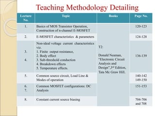
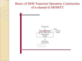
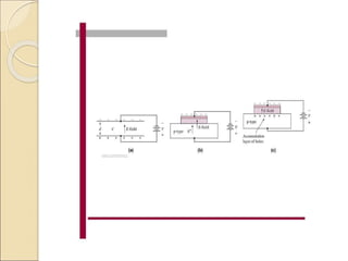
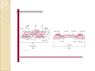
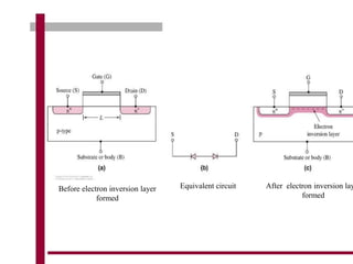
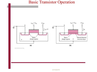
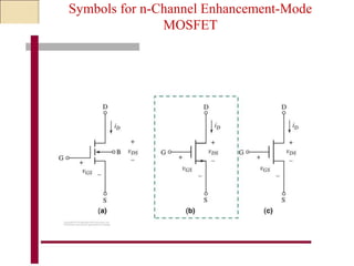
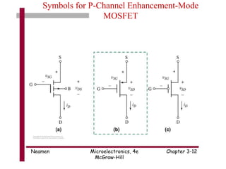
The document discusses MOSFETs and their DC analysis. It covers the basics of MOSFET operation and construction of n-channel enhancement mode MOSFETs. It describes the ideal and non-ideal voltage-current characteristics of MOSFETs including finite output resistance, body effect, subthreshold conduction, and temperature effects. It also discusses common MOSFET configurations like common source circuits and their load lines and modes of operation as well as constant current source biasing.
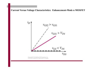
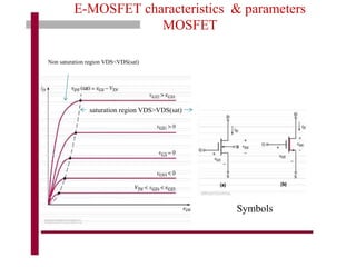
![ Non Saturation or triode region:
VDS< VDS(sat)
Saturation or triode region:
VDS> VDS (sat)
E-MOSFET characteristics & parameters
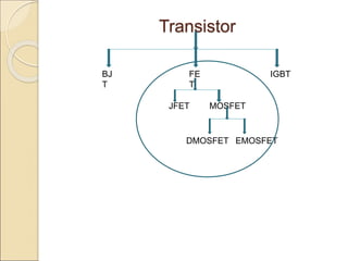
MOSFET
2
2
TNgs
oxn
D VV
C
L
W
i
22
'' TNgsnTNgsnD VVKVVk
L
W
i
])(2[
2
DSGSTNGSnD VVVVKi
L
Wk
ParameterConductionK
n
n
2
,
ox
ox
ox
t
C
](https://image.slidesharecdn.com/mosfetunit2-191128105934/85/Mosfet-unit-2-13-320.jpg)
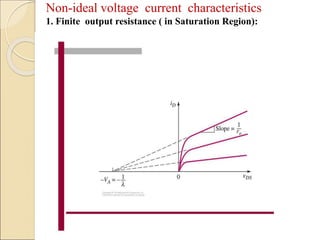
![Non-ideal voltage current characteristics
1. Finite output resistance ( in Saturation Region):
)1...().........1(
2
DSTNGSQnD VVVKi
= Channel Length Modulation Parameter
From above graph the : For ID=0; 0)1( DSV
VDS= - 1/
VDS=-VA
tConsVDS
V
i
ro
DS
D
tan|)( 1
12
][
TNGSQn VVKro
By diff. of equation 1 w.r.to VDS
)2.......(..........
1
][ 1
DQ
A
DQ
DQ
I
V
I
Iro
](https://image.slidesharecdn.com/mosfetunit2-191128105934/85/Mosfet-unit-2-16-320.jpg)


![ppt on IC [Integrated Circuit]](https://cdn.slidesharecdn.com/ss_thumbnails/1-171227170055-thumbnail.jpg?width=640&height=640&fit=bounds)


