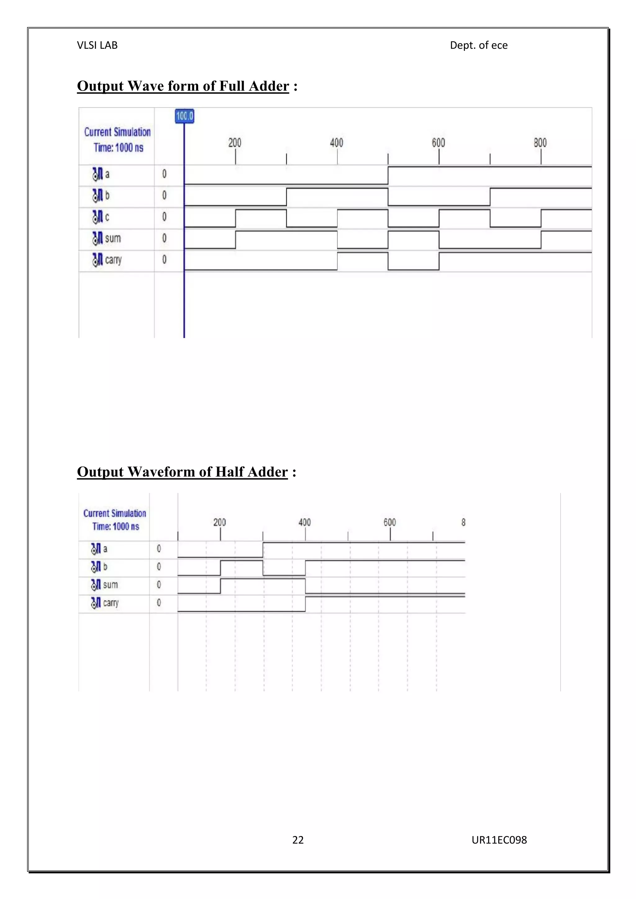
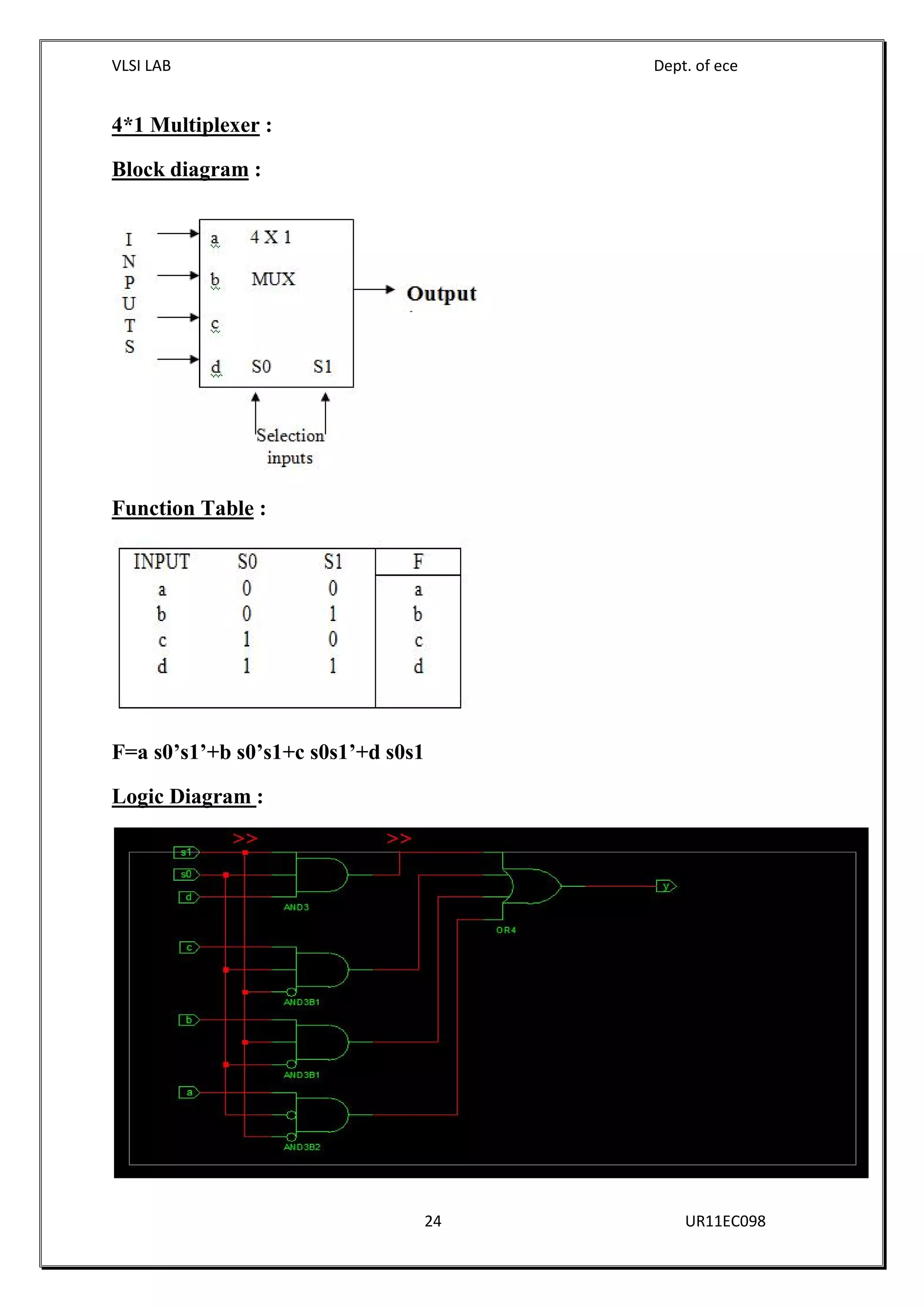
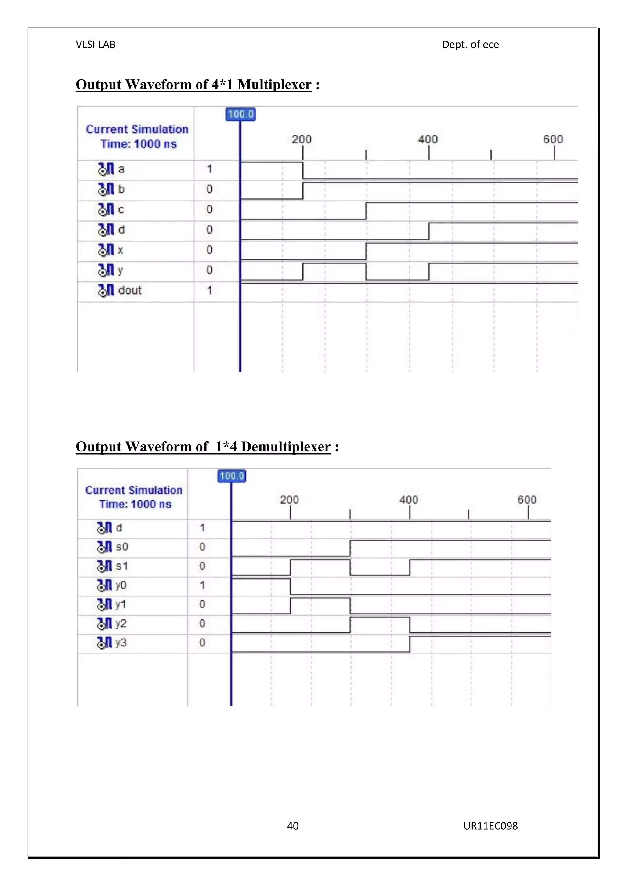
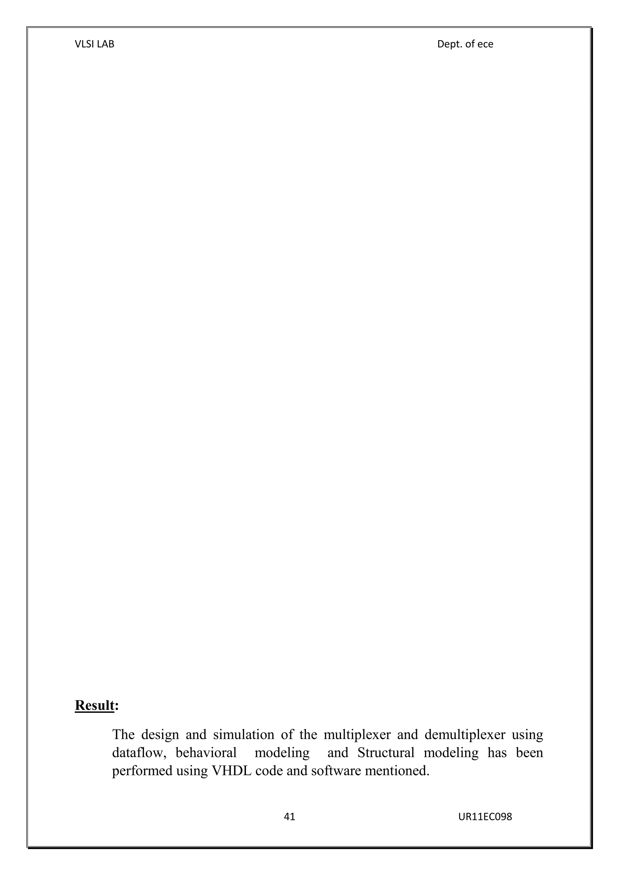
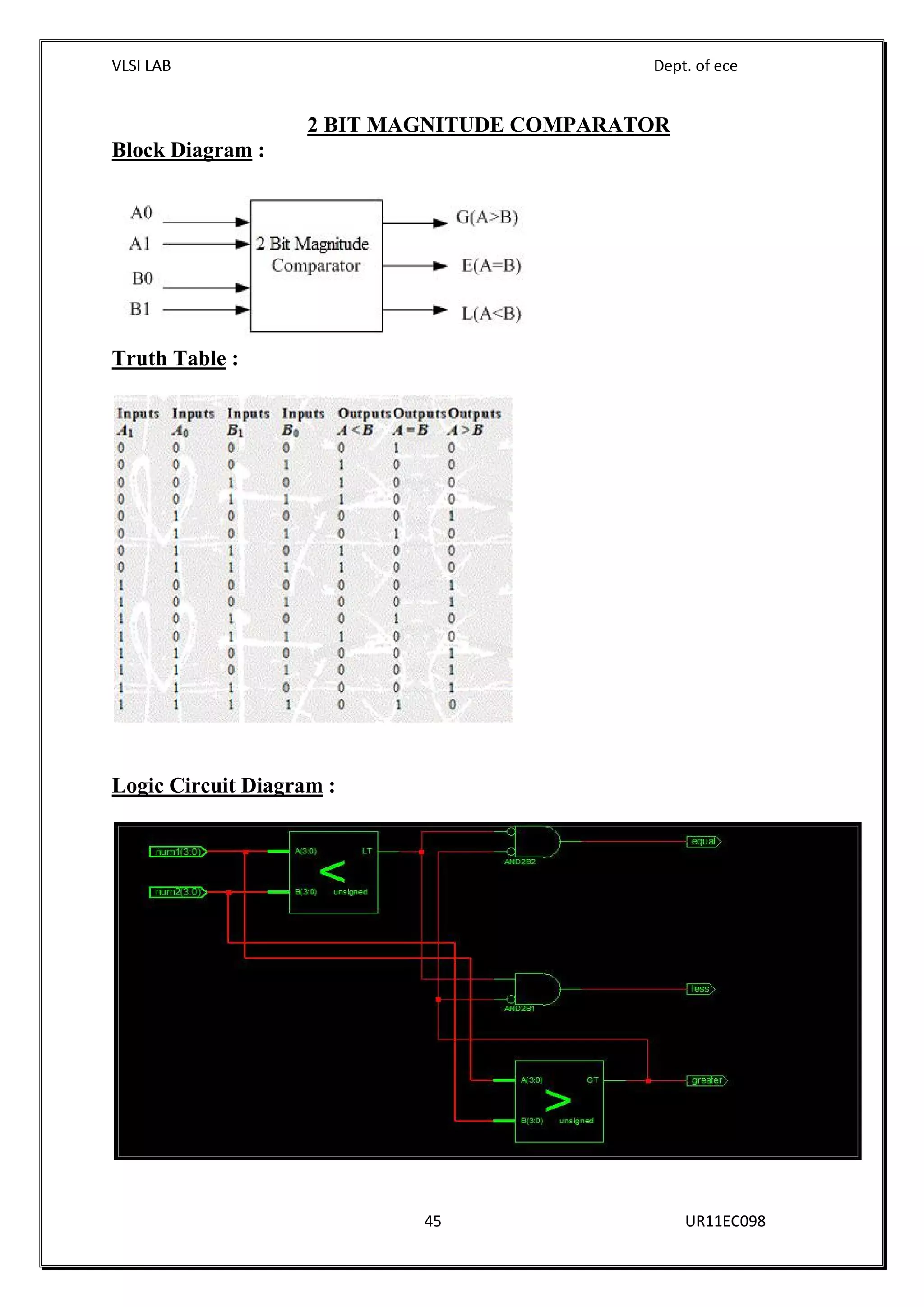
The document describes the design and simulation of half adders, full adders, multiplexers, and demultiplexers using VHDL. It includes block diagrams, truth tables, and VHDL code for implementing these circuits using dataflow, behavioral, and structural modeling in Xilinx ISE. Code examples and output waveforms are provided for half adders, full adders, 4-to-1 multiplexers, and 1-to-4 demultiplexers. The aim is to learn how to design and simulate basic digital circuits using different VHDL modeling approaches.


![VLSI LAB Dept. of ece
89 UR11EC098
AIM:
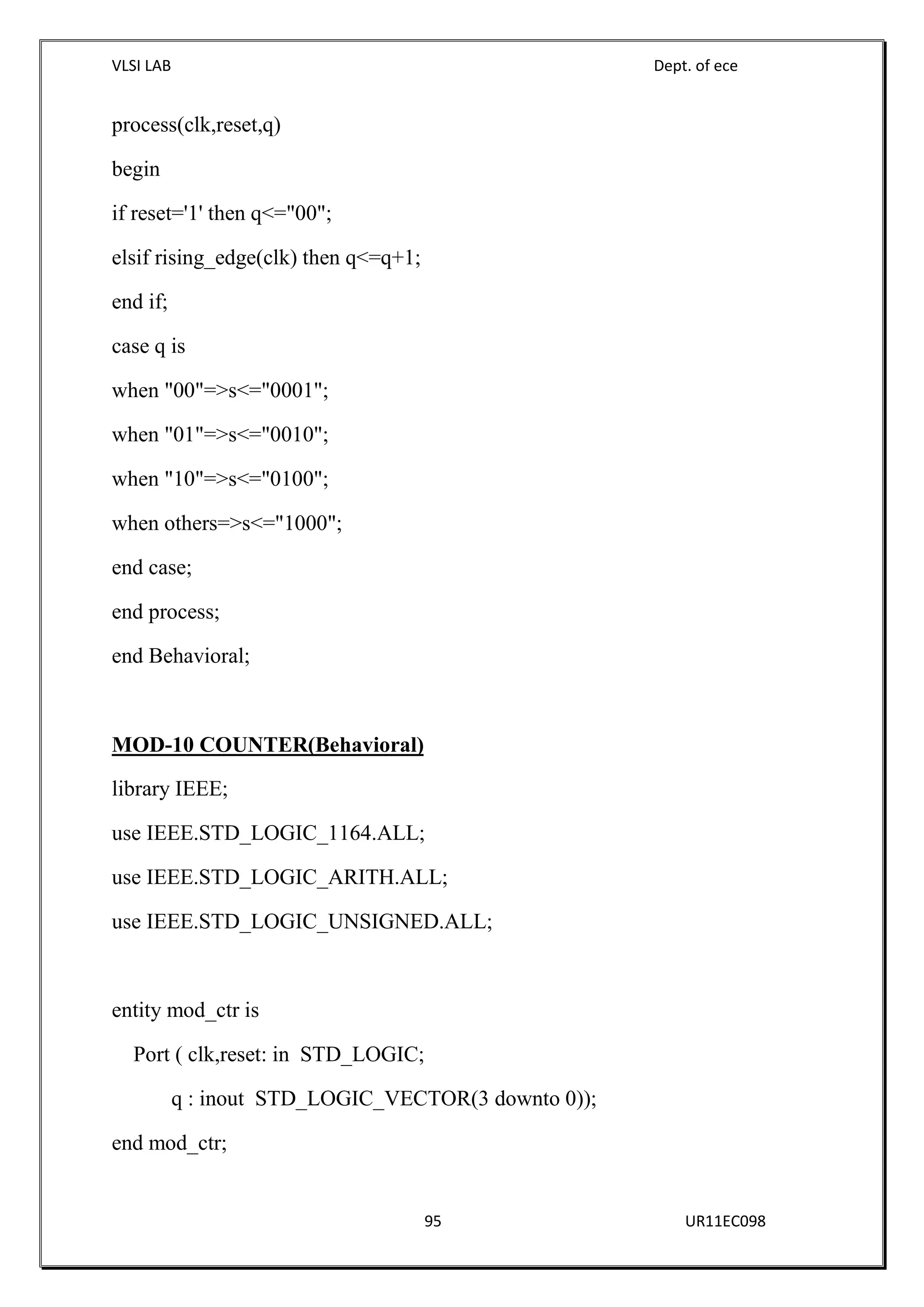
To design and simulate counters [updown,ring & mod10] using behavioral
modeling in VHDL code.
SOFTWARE USED:
Xilinx ISE 14.7
THEORY:
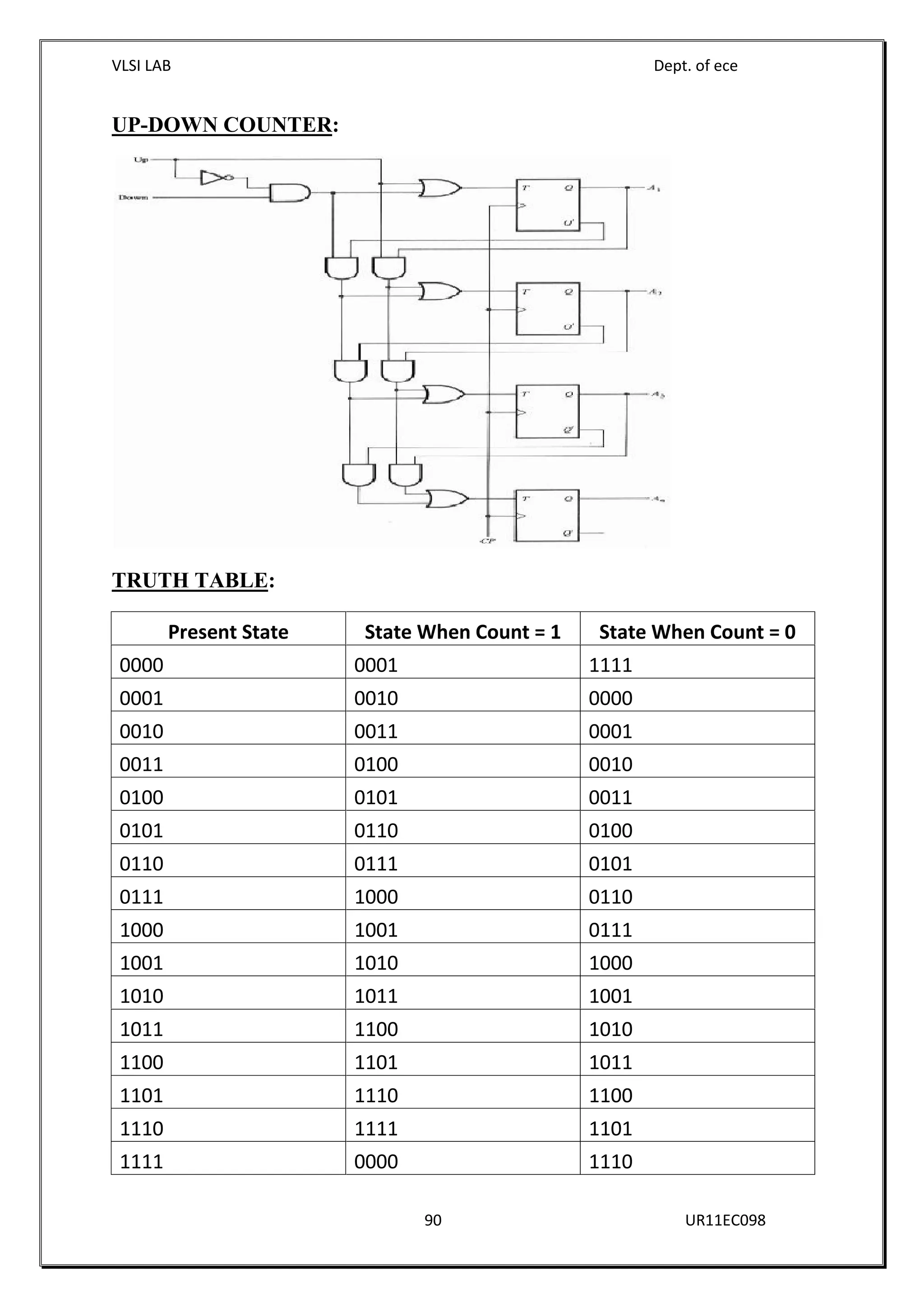
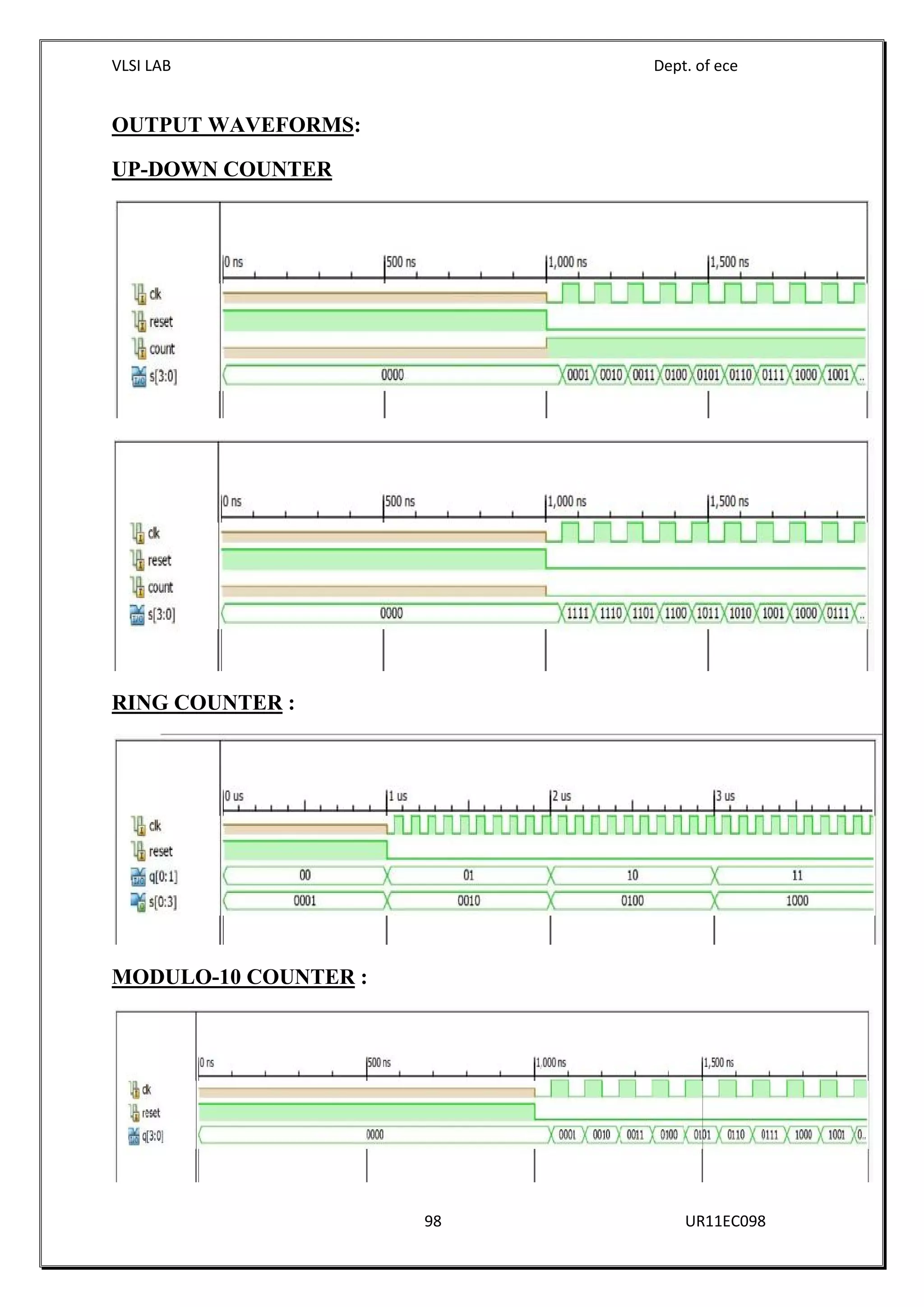
UPDOWN COUNTER
A counter that can change state in either direction, under the control of an up or
down selector input, is known as an up/down counter. When the selector is in
the up state, the counter increments its value. When the selector is in the down
state, the counter decrements the count.
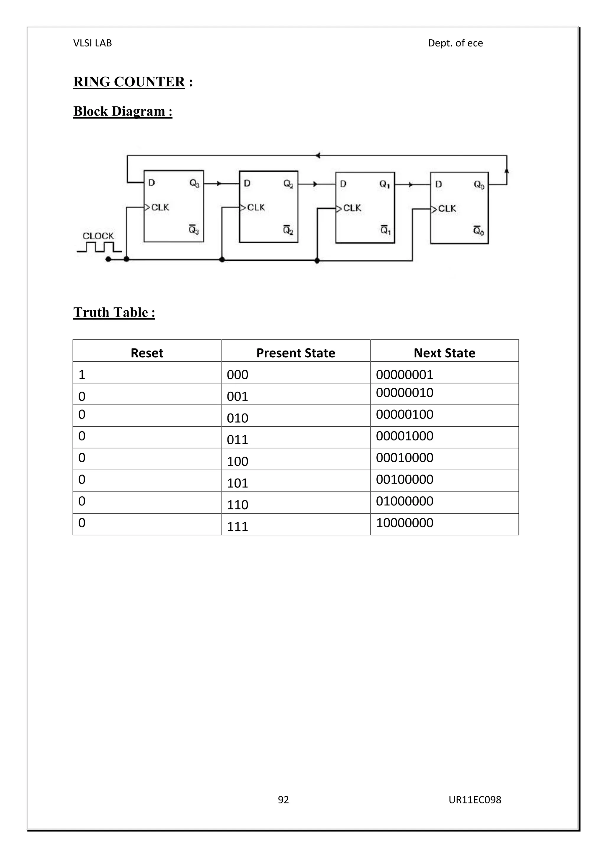
RING COUNTER
A ring counter is a circular shift register which is initiated such that only one of
its flip-flops is the state one while others are in their zero states.
A ring counter is a Shift Register (a cascade connection of flip-flops) with the
output of the last one connected to the input of the first, that is, in a ring.
Typically, a pattern consisting of a single bit is circulated so the state repeats
every n clock cycles if n flip-flops are used. It can be used as a cycle counter of
n states.
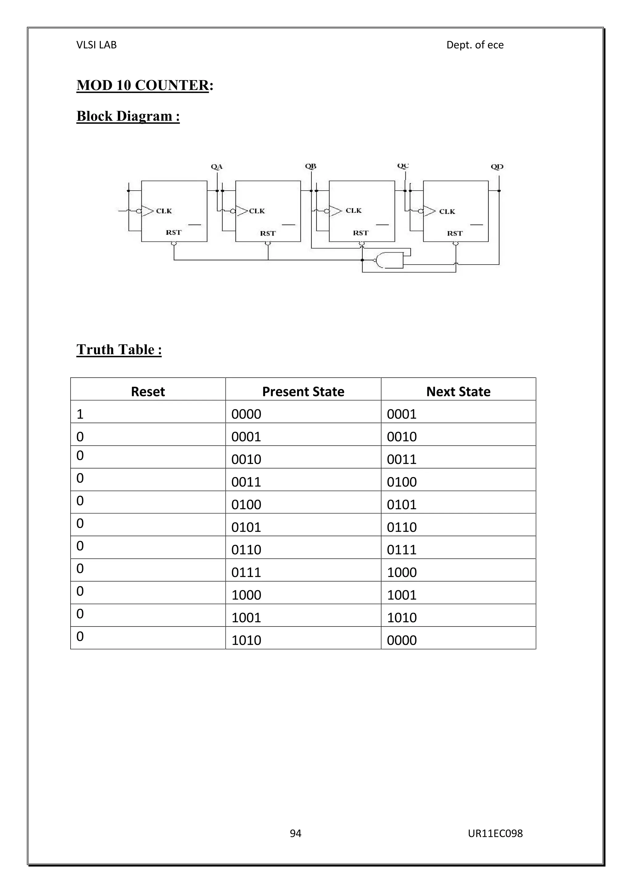
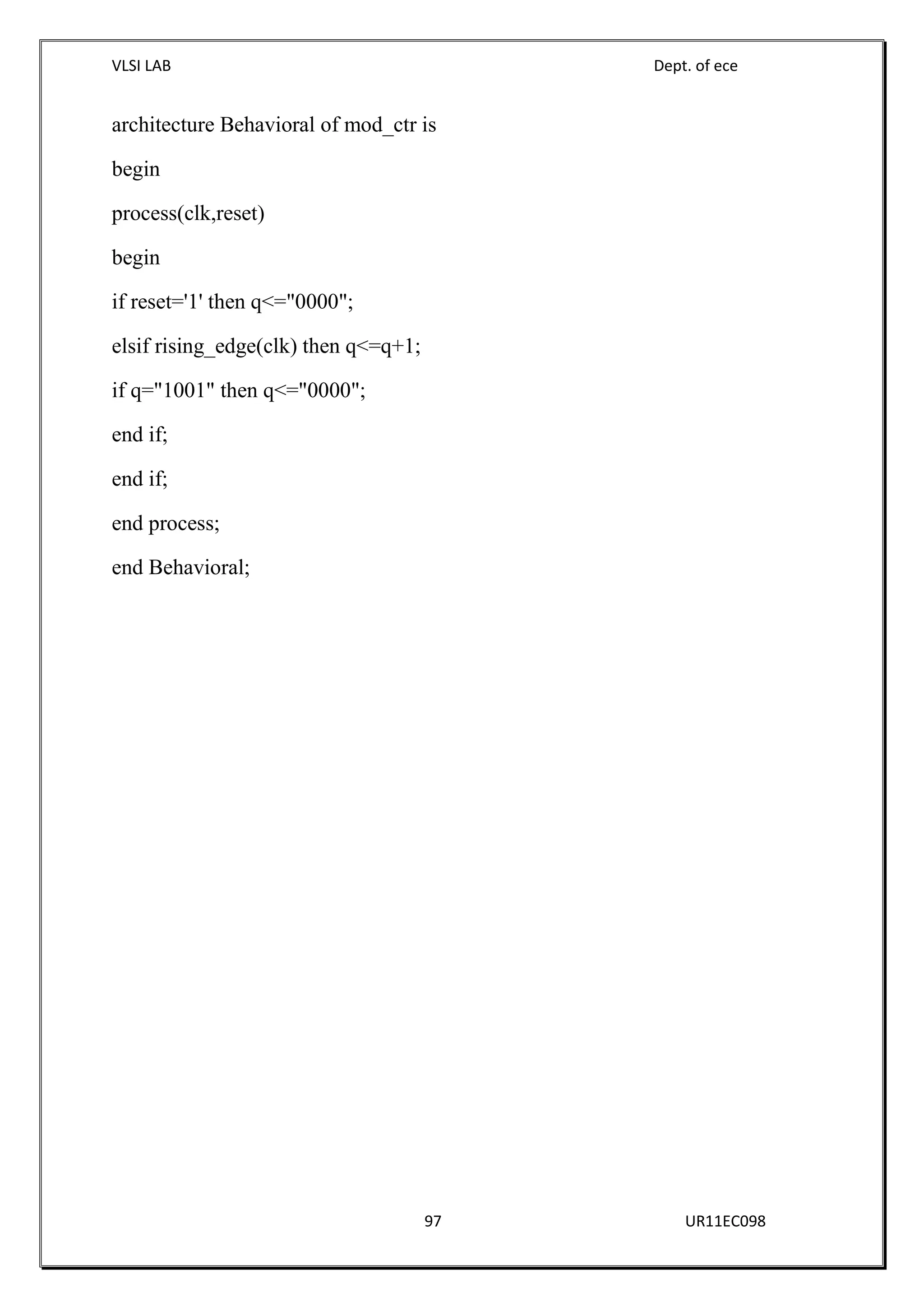
MOD10 COUNTER
A MOD 10 counter has 10 possible states. In other words, it counts from 0 to 9
and rolls over. The decade counter is also known as a mod-counter when it
counts to ten (0, 1, 2, 3, 4, 5, 6, 7, 8, 9). A Mod Counter that counts to 64 stops
at 63 because 0 counts as a valid digit.
Ex No: 6 6.DESIGN AND SIMULATION OF COUNTERS
Date: 19-2-14](https://image.slidesharecdn.com/vlsilab123456789101112exp2-140720055326-phpapp01/75/VLSI-Lab-manual-PDF-89-2048.jpg)