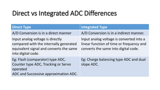
Direct vs Integrated ADC Differences
Direct Type Integrated Type
A/D Conversion is in a direct manner A/D Conversion is in a indirect manner.
Input analog voltage is directly
compared with the internally generated
equivalent signal and converts the same
into digital code.
Input analog voltage is converted into a
linear function of time or frequency and
converts the same into digital code.
Eg: Flash (comparator) type ADC,
Counter type ADC, Tracking or Servo
operated
ADC and Successive approximation ADC.
Eg: Charge balancing type ADC and dual
slope ADC.
Flash ADC
Simultaneous ADC
Parallel Comparator ADC
Condition Comparator Output
Vi > Vref V0 = 1
Vi < Vref V0 = 0
Flash ADC Truth Table
Pros and Cons
• Advantages:
• Flash ADC is the fastest because A/D conversion is performed simultaneously
through a set of comparators. Typical conversion time is 100 ns or less.
• The construction is simple and easier to design.
• Disadvantages:
• This is not suitable for A/D conversion with more than 3 or 4 digital output
bits. It is because of the fact that (2n – 1) comparators are required for an n-bit
ADC and the number of comparators required doubles for each added bit.
Dual Slope ADC
Functional Block Diagram
Description
• Consists of a
1. high impedance buffer (voltage follower), A1
2. integrator, A2
3. voltage comparator (CMP)
• If there is no START command, SW1 is connected to ‘gnd’ and SW2 is
closed. Now CAZ is used to provide compensation for the offset
voltage of all three op-amps.
• If START command is issued, SW2 is connected to ‘gnd’ and SW1 is
connected to Va
.
Description
• At time, t1:
• SW1 is connects Va to A1. SW2 is grounded.
• n-stage counter starts counting from ‘0’ and it resets after
2n clock cycles.
• Va is integrated by the integrator until counter is resetted
(i.e) for a fixed duration of 2n clock periods.
• For an integrator, if the input is a positive step; then the
output is a negative ramp. So, a negative ramp is obtained
across output (V0).
Description
• At time, t2:
• n-stage counter is resetted.
• SW1 connects VR to A1. SW2 is grounded.
• Counter again starts counting from ‘0’.
• VR is integrated by the integrator (a positive ramp is
obtained as VR is positive) until the output voltage (V0) is
zero.
Description
• At time, t3:
• V0 will become ‘0’.
• Now the counter value at t3 , say ‘N’, is proportional to the
analog input voltage, Va.
• EOC is issued by the converter.
Output Waveform
Derivation of V0
• See Notes
Inferences:
• N is directly proportional to Va.
• Provides excellent noise rejection.
• Needs long conversion time.
• Used for accurate measurement of slow varying (less frequency)
signals.
Problem:

ADC_1682318820251.pptx

  • 1.
    Direct vs IntegratedADC Differences Direct Type Integrated Type A/D Conversion is in a direct manner A/D Conversion is in a indirect manner. Input analog voltage is directly compared with the internally generated equivalent signal and converts the same into digital code. Input analog voltage is converted into a linear function of time or frequency and converts the same into digital code. Eg: Flash (comparator) type ADC, Counter type ADC, Tracking or Servo operated ADC and Successive approximation ADC. Eg: Charge balancing type ADC and dual slope ADC.
  • 2.
  • 3.
    Condition Comparator Output Vi> Vref V0 = 1 Vi < Vref V0 = 0
  • 4.
  • 5.
    Pros and Cons •Advantages: • Flash ADC is the fastest because A/D conversion is performed simultaneously through a set of comparators. Typical conversion time is 100 ns or less. • The construction is simple and easier to design. • Disadvantages: • This is not suitable for A/D conversion with more than 3 or 4 digital output bits. It is because of the fact that (2n – 1) comparators are required for an n-bit ADC and the number of comparators required doubles for each added bit.
  • 6.
  • 7.
  • 8.
    Description • Consists ofa 1. high impedance buffer (voltage follower), A1 2. integrator, A2 3. voltage comparator (CMP) • If there is no START command, SW1 is connected to ‘gnd’ and SW2 is closed. Now CAZ is used to provide compensation for the offset voltage of all three op-amps. • If START command is issued, SW2 is connected to ‘gnd’ and SW1 is connected to Va .
  • 9.
    Description • At time,t1: • SW1 is connects Va to A1. SW2 is grounded. • n-stage counter starts counting from ‘0’ and it resets after 2n clock cycles. • Va is integrated by the integrator until counter is resetted (i.e) for a fixed duration of 2n clock periods. • For an integrator, if the input is a positive step; then the output is a negative ramp. So, a negative ramp is obtained across output (V0).
  • 10.
    Description • At time,t2: • n-stage counter is resetted. • SW1 connects VR to A1. SW2 is grounded. • Counter again starts counting from ‘0’. • VR is integrated by the integrator (a positive ramp is obtained as VR is positive) until the output voltage (V0) is zero.
  • 11.
    Description • At time,t3: • V0 will become ‘0’. • Now the counter value at t3 , say ‘N’, is proportional to the analog input voltage, Va. • EOC is issued by the converter.
  • 12.
  • 13.
  • 14.
    Inferences: • N isdirectly proportional to Va. • Provides excellent noise rejection. • Needs long conversion time. • Used for accurate measurement of slow varying (less frequency) signals.
  • 15.