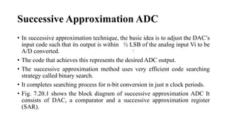
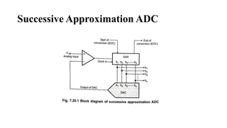
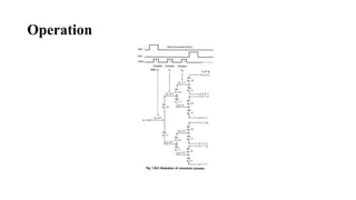
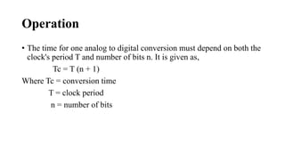
Successive
Approximation ADC
Dr.R.Hepzi Pramila Devamani,
Assistant Professor of Physics,
V.V.Vanniaperumal College for Women,
Virudhunagar.
Successive Approximation ADC
‱ In successive approximation technique, the basic idea is to adjust the DAC’s
input code such that its output is within œ LSB of the analog input Vi to be
A/D converted.
‱ The code that achieves this represents the desired ADC output.
‱ The successive approximation method uses very efficient code searching
strategy called binary search.
‱ It completes searching process for n-bit conversion in just n clock periods.
‱ Fig. 7.20.1 shows the block diagram of successive approximation ADC It
consists of DAC, a comparator and a successive approximation register
(SAR).
Successive Approximation ADC
‱ The external clock input sets the internal timing parameters.
‱ The control signal start of conversion (SOC) initiates an A/D
conversion process and end of conversion signal is activated when the
conversion is completed.
Operation
‱ The searching code process in successive approximation method is
similar to weighing an unknown material with a balance scale and a
set of standard weights.
‱ Let us assume that we have 1 kg, 2 kg and 4 kg weights (SAR) plus a
balance scale (comparator and DAC).
‱ The successive approximation analogy for 3-bit ADC can be
discussed.
Operation
‱ Refer Fig. 7.20.1 and 7.20.2. The analog voltage Vin is applied at one input of comparator.
‱ On receiving start of conversion signal (SOC) successive approximation register sets 3-bit binary
code 100₂, (b₂ = 1) as an input of DAC.
‱ This is similar process of placing the unknown weight on one platform of the balance and 4 kg
weight on the other.
‱ The DAC converts the digital word 100 and applies it equivalent analog output at the second input
of the comparator.
‱ The comparator then compares two voltages just like comparing unknown weight with 4 kg weight
with the help of balance scale.
‱ If the input voltage is greater than the analog output of DAC, successive approximation register
keeps b₂ = 1 and makes b1 = 1 (addition of 2 kg weight) otherwise it resets b₂ = 0 and makes to
have total 6 kg weight) otherwise it resets b₂ = 0 and makes b₁ =1 (replacing 2 kg weight).
‱ The same process is repeated for b1 and b2. The status of b0, b1 and b2 bits gives the digital
equivalent of the analog input.
Operation
Operation
‱ The dark lines in the Fig. 7.20.2 shows setting and resetting actions of
bits for input voltage 5.2 V, on the basis of comparison.
‱ It can be seen from the Fig. 7.20.2 that one clock pulse is required for
the successive approximation register to compare each bit.
‱ However an additional clock pulse is usually required to reset the
register prior to performing a conversion.
Operation
‱ The time for one analog to digital conversion must depend on both the
clock's period T and number of bits n. It is given as,
Tc = T (n + 1)
Where Tc = conversion time
T = clock period
n = number of bits
THANK YOU

Successive Approximation ADC.pptx

  • 1.
    Successive Approximation ADC Dr.R.Hepzi PramilaDevamani, Assistant Professor of Physics, V.V.Vanniaperumal College for Women, Virudhunagar.
  • 2.
    Successive Approximation ADC ‱In successive approximation technique, the basic idea is to adjust the DAC’s input code such that its output is within œ LSB of the analog input Vi to be A/D converted. ‱ The code that achieves this represents the desired ADC output. ‱ The successive approximation method uses very efficient code searching strategy called binary search. ‱ It completes searching process for n-bit conversion in just n clock periods. ‱ Fig. 7.20.1 shows the block diagram of successive approximation ADC It consists of DAC, a comparator and a successive approximation register (SAR).
  • 3.
  • 4.
    Successive Approximation ADC ‱The external clock input sets the internal timing parameters. ‱ The control signal start of conversion (SOC) initiates an A/D conversion process and end of conversion signal is activated when the conversion is completed.
  • 5.
    Operation ‱ The searchingcode process in successive approximation method is similar to weighing an unknown material with a balance scale and a set of standard weights. ‱ Let us assume that we have 1 kg, 2 kg and 4 kg weights (SAR) plus a balance scale (comparator and DAC). ‱ The successive approximation analogy for 3-bit ADC can be discussed.
  • 6.
    Operation ‱ Refer Fig.7.20.1 and 7.20.2. The analog voltage Vin is applied at one input of comparator. ‱ On receiving start of conversion signal (SOC) successive approximation register sets 3-bit binary code 100₂, (b₂ = 1) as an input of DAC. ‱ This is similar process of placing the unknown weight on one platform of the balance and 4 kg weight on the other. ‱ The DAC converts the digital word 100 and applies it equivalent analog output at the second input of the comparator. ‱ The comparator then compares two voltages just like comparing unknown weight with 4 kg weight with the help of balance scale. ‱ If the input voltage is greater than the analog output of DAC, successive approximation register keeps b₂ = 1 and makes b1 = 1 (addition of 2 kg weight) otherwise it resets b₂ = 0 and makes to have total 6 kg weight) otherwise it resets b₂ = 0 and makes b₁ =1 (replacing 2 kg weight). ‱ The same process is repeated for b1 and b2. The status of b0, b1 and b2 bits gives the digital equivalent of the analog input.
  • 7.
  • 8.
    Operation ‱ The darklines in the Fig. 7.20.2 shows setting and resetting actions of bits for input voltage 5.2 V, on the basis of comparison. ‱ It can be seen from the Fig. 7.20.2 that one clock pulse is required for the successive approximation register to compare each bit. ‱ However an additional clock pulse is usually required to reset the register prior to performing a conversion.
  • 9.
    Operation ‱ The timefor one analog to digital conversion must depend on both the clock's period T and number of bits n. It is given as, Tc = T (n + 1) Where Tc = conversion time T = clock period n = number of bits
  • 10.