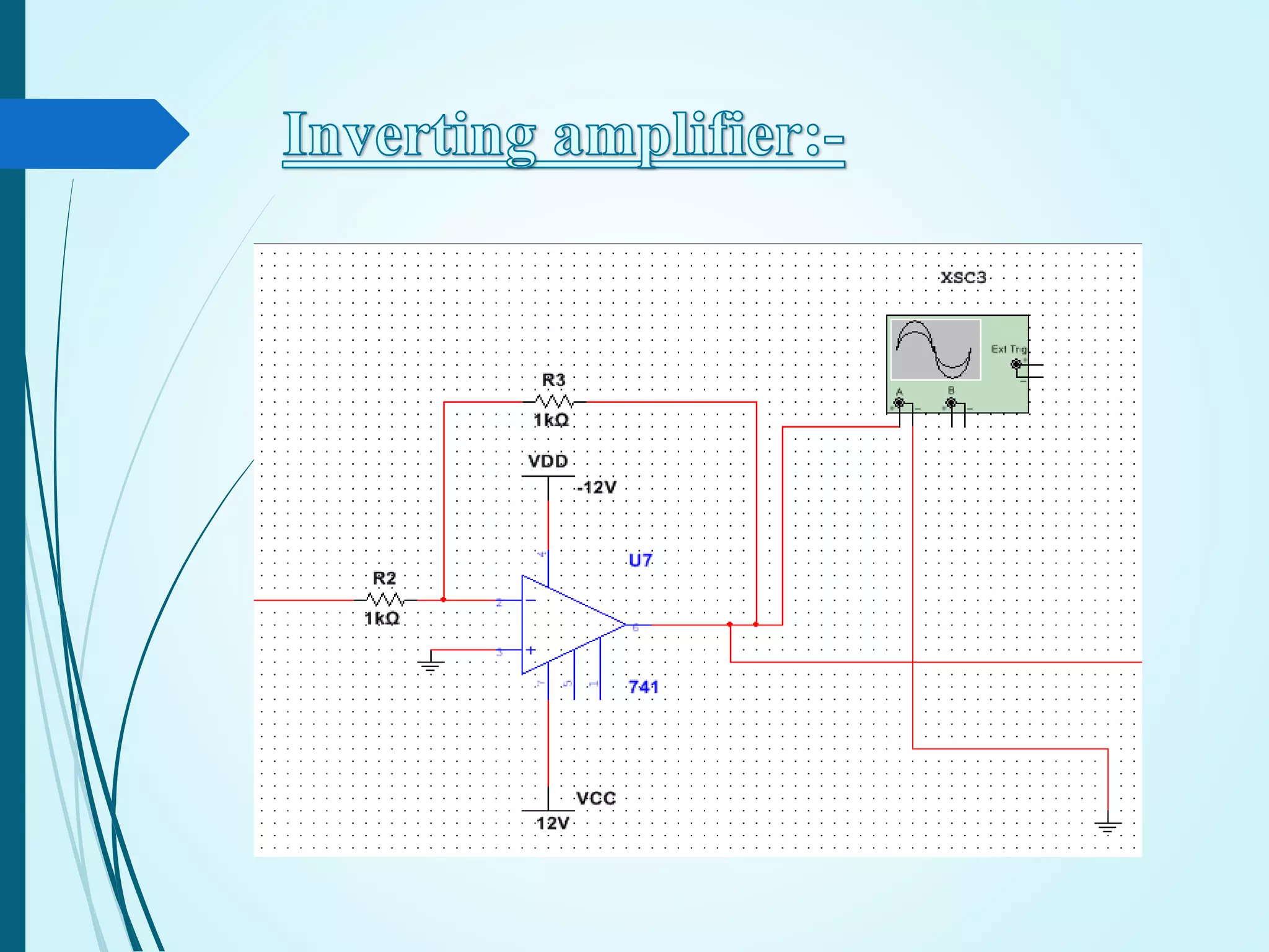
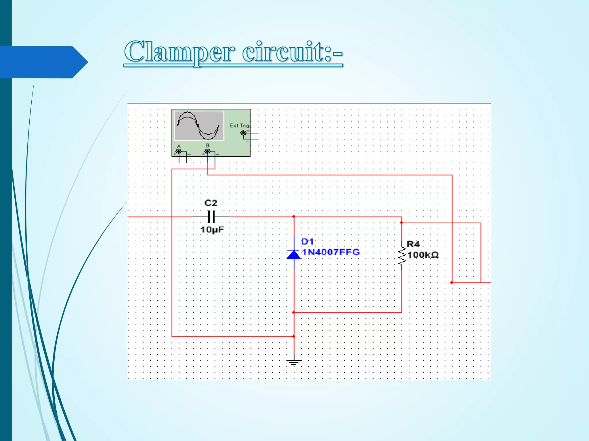
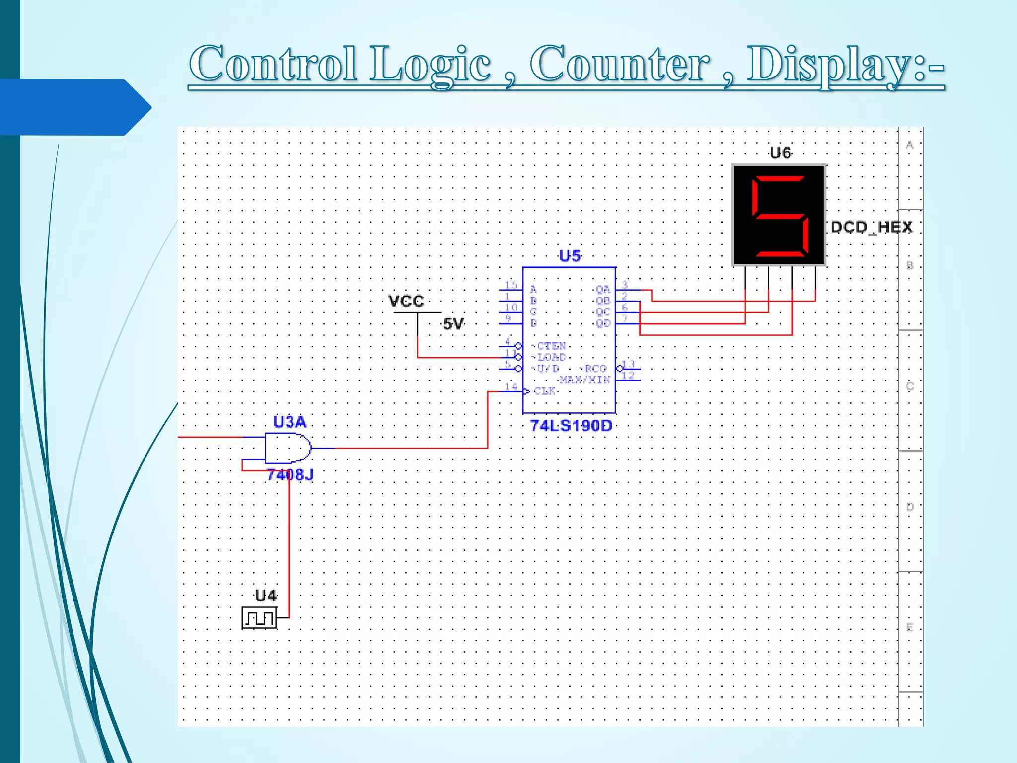
PRESENTED BY:-
1. Introduction
2. Circuit diagram
3. Working with design
4. Tool
5. Expected output
6. Applications
7. Advantages and disadvantages
8. References
In this project, we designed and implemented a
analog to digital converter using single slope ADC
technique.
 Integrator
 Sample and hold circuit
 Comparator
 Control logic
 Counter
 Display
 A counter determines the number of clock pulses that are
required before the integrated value of a reference voltage
is equal to the sampled input signal.
 The number of clock pulses is proportional to the actual
value of the input
 The output of the counter is the actual digital represntation
of the analog voltage
 Since the reference is a dc voltage the output of the
integrator should start at zero
 linearly increase with a slope that depends on the gain of
the integrator
The integrator output voltage V1 rises
until it reaches Vsampled value. Hence the
conversion time tc is equal to:
 Used in high-resolution applications
 Commonly found in slow-speed, low cost
applications
 Digital multi-meters
 Panel meters
 Voltage or current meters
 Monitoring DC signals in the instrumentation and
industrial markets
 Resolution:
 Able To Achieve 14 Bits Or Higher
 Very Inexpensive To Produce
 Low Power Consumption
 Very Low Offset And Gain Errors
 Highly Linear
 Good Noise Performance
Slow Conversion
Typically Less Than A Few Hundred Samples
Per Second
Sensitive (Direct Dependence Of The
Digital Output) To The Values Of:
Resistor R1
Capacitor C1
Negative Reference Voltage -VREF
 Baker R. Jacob, CMOS Circuit Design, Layout, and
Simulation, 3rd Edition, 2010, John Wiley & Sons
 http://cmosedu.com/jbaker/courses/ece614/s08/lec26_ece
614.pdf
ADC using single slope  technique

ADC using single slope technique

  • 1.
  • 2.
    1. Introduction 2. Circuitdiagram 3. Working with design 4. Tool 5. Expected output 6. Applications 7. Advantages and disadvantages 8. References
  • 3.
    In this project,we designed and implemented a analog to digital converter using single slope ADC technique.
  • 4.
     Integrator  Sampleand hold circuit  Comparator  Control logic  Counter  Display
  • 6.
     A counterdetermines the number of clock pulses that are required before the integrated value of a reference voltage is equal to the sampled input signal.  The number of clock pulses is proportional to the actual value of the input  The output of the counter is the actual digital represntation of the analog voltage  Since the reference is a dc voltage the output of the integrator should start at zero  linearly increase with a slope that depends on the gain of the integrator
  • 18.
    The integrator outputvoltage V1 rises until it reaches Vsampled value. Hence the conversion time tc is equal to:
  • 20.
     Used inhigh-resolution applications  Commonly found in slow-speed, low cost applications  Digital multi-meters  Panel meters  Voltage or current meters  Monitoring DC signals in the instrumentation and industrial markets
  • 21.
     Resolution:  AbleTo Achieve 14 Bits Or Higher  Very Inexpensive To Produce  Low Power Consumption  Very Low Offset And Gain Errors  Highly Linear  Good Noise Performance
  • 22.
    Slow Conversion Typically LessThan A Few Hundred Samples Per Second Sensitive (Direct Dependence Of The Digital Output) To The Values Of: Resistor R1 Capacitor C1 Negative Reference Voltage -VREF
  • 23.
     Baker R.Jacob, CMOS Circuit Design, Layout, and Simulation, 3rd Edition, 2010, John Wiley & Sons  http://cmosedu.com/jbaker/courses/ece614/s08/lec26_ece 614.pdf