Download to read offline
![International Journal of VLSI design & Communication Systems (VLSICS) Vol.4, No.3, June 2013
DOI : 10.5121/vlsic.2013.4310 102
DESIGN AND PERFORMANCE ANALYSIS OF ZBT
SRAM CONTROLLER
Smriti Sharma1
and Balwinder Singh2
1,2
Centre for Development of Advanced Computing, India
Sharma.smriti21@gmail.com, Balwinder.cdacmohali@gmail.com
ABSTRACT
Memory is an essential part of electronic industry. Since, the processors used in various high performance
PCs, network applications and communication equipment require high speed memories. The type of
memory used depends on system architecture, and its applications. This paper presents an SRAM
architecture known as Zero Bus Turnaround (ZBT). This ZBT SRAM is mainly developed for networking
applications where frequent READ/WRITE transitions are required. The other single data rate SRAMs are
inefficient as they require idle cycles when they frequently switch between reading and writing to the
memory. This controller is simulated on the Spartan 3 device. And the performance analysis is done on the
basis of area, speed and power.
KEYWORDS
ZBT SRAM, performance analysis, READ/WRITE transitions, speed, area & power
1. INTRODUCTION
The emergence of networking and communication systems requiring higher bandwidth interfaces
and lower latency for peripheral components lead to the implementation of designs using high
throughput memory with efficient bus utilization and resulted in the development of a new SRAM
architecture known as ZBT. The previous generation of static memory types is inefficient as they
require idle cycles when they frequently switch between reading from and writing to the memory.
IDT, Micron, and Motorola have developed the ZBT SRAM architecture to address this problem.
ZBT SRAM is offered with two intefaces they are: Flowthrough and Pipelined SRAM. Pipelined
interface requires two clock cycles for read and two clock cycles for write operations where as
flowthrough requires single clock cycle for both read and write operation, respectively.
Flowthrough provides one clock cycle less latency then pipelining, where as pipelining provides
high clock to data access.
Due to the fast, low latency access to the CPU, SRAMS are widely used in data communication
systems. ZBT SRAM architecture was developed to improve the bandwidth of the interface and
overcome the several limitations. ZBT SRAM technology was developed for operation in the
applications where data rates are below 200MHz.
Synchronous SRAM basically comes under two different flavors: Single data rate SRAMs and
Double data rate SRAMs [5].](https://image.slidesharecdn.com/vlsics040310-130712042732-phpapp01/75/DESIGN-AND-PERFORMANCE-ANALYSIS-OF-ZBT-SRAM-CONTROLLER-1-2048.jpg)
![International Journal of VLSI design & Communication Systems (VLSICS) Vol.4, No.3, June 2013
102
The single Data Rate SRAMs are:
• Pipelined vs. Flowthrough SRAMs
• Burst SRAMs
• Network SRAMs - NoBL™/ZBT™ SRAMs.
The Double Data Rate SRAMs are:
• Standard DDR SRAMs
• QDR™ SRAMs.
Table 1. Comparison of ZBT/NoBL SRAM with other single data rate synchronous SRAMs
2. ZBT SRAM CONTROLLER
2.1. A Primer on ZBT SRAM
The term "Zero Bus Turnaround" was invented by IDT in October 1996. IDT, Micron, and
Motorola are the three companies that developed the ZBT technologies independently, and are
offering compatible ZBT products based upon the same architecture. ZBT SRAM provides the
maximum system throughput by utilizing every bus cycles. There is no turnaround cycles when
switching between read and write cycles. So this feature is beneficial in various applications with
random, intermixed read and writes operations on the data bus as compared to long bursts of
reads and writes. Some of the applications are LAN and WAN switching, gigabit switching,
network interface cards, ATM switching, switch or hub-shared fabric and router tables. ZBT
SRAM comes in two varieties i.e. pipelined and flowthrough. Flowthrough devices have shorter
latency than pipelined devices, but pipelined devices can operate at higher frequencies. Control
signals on both types are identical, and are simpler than Sync Burst. Pipelined ZBT SRAMs are
late-late-read RAMs in the sense that data appears two clock cycles after address. In order to
allow interleaved reads and writes, it is also called late-late-write RAM. Flowthrough ZBT
SRAM is late-read RAMs in that data appears one clock cycle after address. They are also called
late-write RAMs [10].
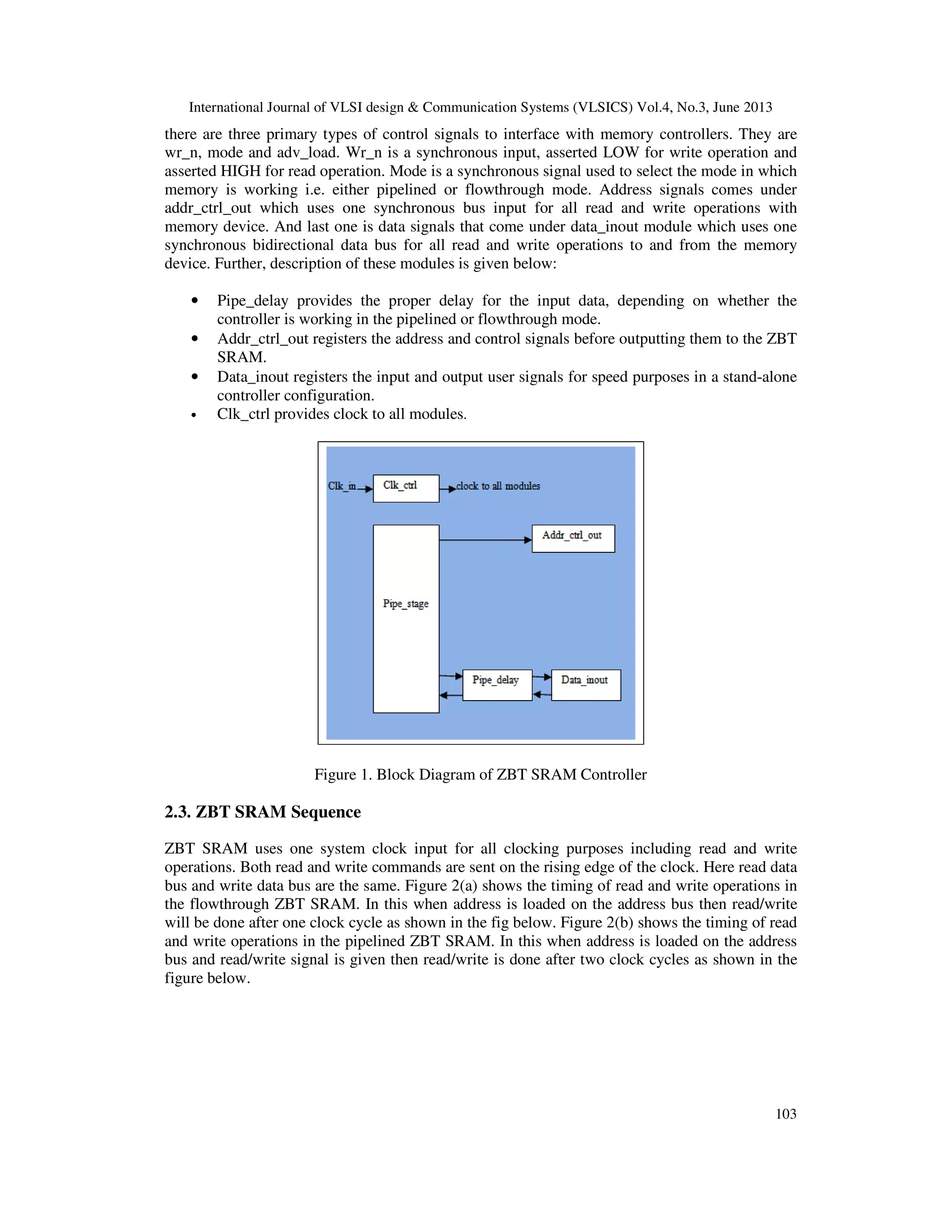
2.2. Block Diagram of ZBT SRAM Controller
In figure 1, the various low level modules of ZBT SRAM Controller are shown. An overview of
various signals used in ZBT SRAM controller are control, clock, address and data signals to give
an overall functionality description. The ZBT SRAM controller accepts SRAM request from user
and performs pipelined or flowthrough read and write operations, respectively. The controller
ensures that correct latencies and bus turnaround timings are met. Clock signal which comes
under the module clk_ctrl is used for all clocking purposes including reads and writes. All these
timing references are made at the rising edge of clock. Pipe_stage covers the control signals, and
Other Single Data Rate
Synchronous SRAMs
ZBT/NoBL Synchronous
SRAM
Most effective for Burst
Reads/Writes for Level 2 Cache
Ideal for Networking
applications
Ideal for Dominated Read or
Write
Ideal for Read/Write ratio
of 1
Latency occurs when switching
from write to read operation
Enables faster memory
performance-eliminates the
latency cycle](https://image.slidesharecdn.com/vlsics040310-130712042732-phpapp01/75/DESIGN-AND-PERFORMANCE-ANALYSIS-OF-ZBT-SRAM-CONTROLLER-2-2048.jpg)
![International Journal of VLSI design & Communication Systems (VLSICS) Vol.4, No.3, June 2013
104
Figure 2(a): Flowthrough operation
Figure 2(b): Pipelined Operation
3. RELATED WORK
Many researchers have explored the reading and writing from and to the memory in the past with
different SRAMs memory architectures and controllers designed. Some of the papers and
datasheets are discussed below. Kang Li et. al. [2] proposed a new architecture of shared QDR
SRAM controller to make the SRAM Controller suitable for higher bandwidth and speed network
communication. In this arbitration method is used to simultaneous read and write operation to the
memory can be executed, and tag architecture is adopted to keep the special sequence of the
SRAM reference. Thus, the high utilization of bandwidth is done. Ravi Khatwal [1] has worked
to design high speed and low power consumption memory for embedded system. And by using
Xilinx tool, they calculate the access time that is required for selecting a word and reading it. In
this, synchronous static RAM has easily read/writes operation in efficient manner. Abhishek
kumar et. al. [4] has worked to design a kind of SDRAM controller. This controller provides a
synchronous command interface to the SDRAM memory along with several control signals. It has
two main control schemes, command generation and signal generation, simultaneously these
modules provide signal to the data path for data transfer. In this memory system operates at
double the frequency of processor, without affecting the performance, we can reduce the data bus
size. Ranjan Chakraborty [3] discusses about the design of an 8-bit First In First Out Memory
which may be utilized in various electronic components and gadgets. In the first stage of design,
the RAM 16X4S chips are introduced in the design but here the numbers of bits were reduced
from 16 to 8 as it was not being possible to carry the previous number of bits in this renewed
design.
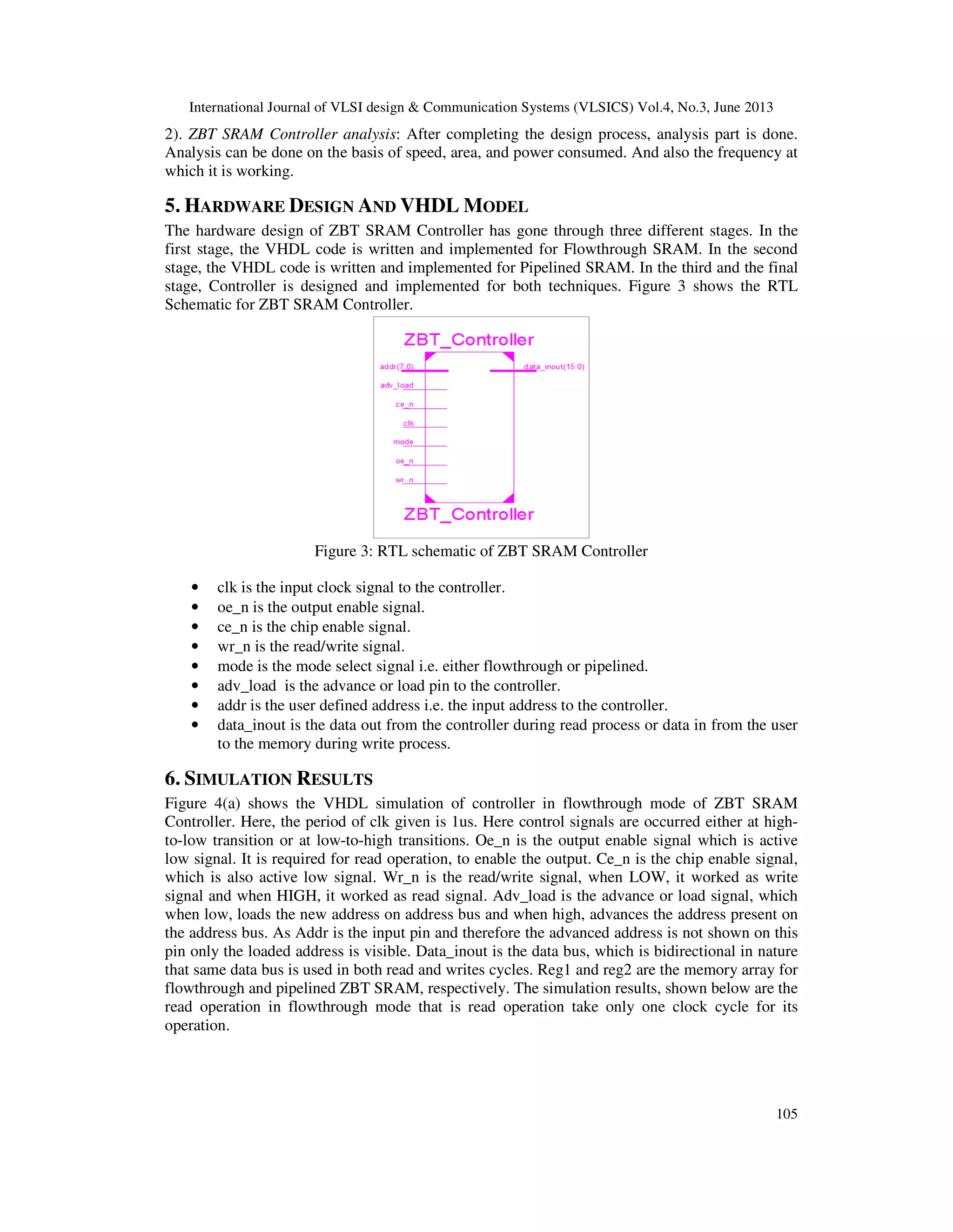
4. PROPOSED WORK
The design of the ZBT SRAM controller has been done successfully on Xilinx ISE Design Suite
12.4. The main contributions of this work are as follows:
1). ZBT SRAM Controller design: At first, we have to understand the working of address module.
Secondly, the most important block is datapath module, the most difficult aspect of ZBT SRAM
controller design is to transmit and capture data at proper time delay according to the mode
selected.](https://image.slidesharecdn.com/vlsics040310-130712042732-phpapp01/75/DESIGN-AND-PERFORMANCE-ANALYSIS-OF-ZBT-SRAM-CONTROLLER-4-2048.jpg)
![International Journal of VLSI design & Communication Systems (VLSICS) Vol.4, No.3, June 2013
107
Table 2(b): Timing Summary
Timing ZBT SRAM
Controller
Speed Grade -4
Minimum period 5.007ns
Maximum Frequency 199.720MHz
Minimum input arrival time before clock 6.598ns
Maximum output required time after clock 11.325ns
Maximum combinational path delay 12.538ns
8. CONCLUSIONS
In this paper, we have designed various modules of ZBT SRAM Controller and verified the
required functionality by using test bench. The main challenging part is to meet all the timing
requirements of various modules. We have met all the timing requirements efficiently. All the
design features are met according to the requirements. The device utilization summary is given in
Table2 (a) and timing summary is given in Table2 (b). And the total power consumed is 243.76
mW.
REFERENCES
[1] Ravi Khatwal and Manoj Kumar Jain. Article, March 2013: “An Efficient Synchronous Static
Memory design for Embedded System”. International Journal of Computer Applications 66(18):39-
45. Published by Foundation of Computer Science, New York, USA.
[2] Kang Li; Hongye Jia; Honghu Gong; Jiangyi Shi; Peijun Ma, 28-30 Oct. 2011 "Optimization of QDR
SRAM Controller in Network Processor," Computational Intelligence and Design (ISCID), 2011
Fourth International Symposium on , vol.1, pp.254-257. DOI :10.1109/ISCID.2011.71
[3] Ranjan Chakraborty, July 6-8, 2011 “Design and implementation of 8-bit read-write memory using
FIFO Algorithm,” Proceedings of the World Congress on Engineering 2011 Vol II WCE 2011,
London, U.K.
[4] Abhishek Kumar, Yogesh. E. Wankhede, Kirti Shinde P., Nisha Sarwade, 2010 “Design of SDRAM
Memory Controller using VHDL,” International Journal of Computer Science and Application Issue,
pp. 184-189, ISSN 0974-0767.
[5] Application Note, 2006 “Introduction to Cypress SRAMs – AN1116”.
[6] Volnei A. Pedroni, 2004 “Circuit Design with VHDL”, MIT Press Cambridge, Massachusetts
London, England.
[7] Altera, 2004 “ZBT SRAM Controller Reference Design for Stratix & Stratix GX Devices”.
[8] JOHN F. WAKERLY, 2002 “Digital design principles & practices”, 3rd Edition, Pearson Education
Asia.
[9] Shekhar Bapat, January 10, 2000 “Synthesizable 200 MHz ZBT SRAM Interface,” XAPP136 (v2.0).
[10] Shekhar Bapat, April 6, 1999 “Synthesizable 143 MHz ZBT* SRAM Interface,” XAPP136, (Version
1.1).
[11] Datasheet for ZBT SRAM Controller, Softjin enabling electronic design.](https://image.slidesharecdn.com/vlsics040310-130712042732-phpapp01/75/DESIGN-AND-PERFORMANCE-ANALYSIS-OF-ZBT-SRAM-CONTROLLER-7-2048.jpg)
![International Journal of VLSI design & Communication Systems (VLSICS) Vol.4, No.3, June 2013
108
[12] Application Note, 1997 “Understanding Static RAM Operation
Authors Biography
Balwinder Singh has obtained his Bachelor of Technology degree from National
Institute of Technology, Jalandhar and Master of Technology degree from University
Centre for Inst. & Microelectronics (UCIM), Punjab University, Chandigarh in 2002 and
2004 respectively. He is currently serving as Senior Engineer in Centre for Development
of Advanced Computing (CDAC), Mohali and is a part of the teaching faculty and also
pursuing PhD from GNDU Amritsar. He has 8+ years of teaching experience to both
undergraduate and postgraduate students. Singh has published three books and many papers in the
International & National Journal and Conferences. His current interest includes Genetic algorithms, Low
Power techniques, VLSI Design & Testing, and System on Chip.
Smriti Sharma received the B.Tech (Electronics and Communication Engineering)
degree from the Inderprastha Engineering College, Sahibabad affiliated to Uttar Pradesh
Technical University, in 2009, and presently she is doing M.Tech (VLSI design) degree
from Centre for Development of Advanced Computing (CDAC), Mohali and working on
her thesis work. Her area of interest is VLSI Design.](https://image.slidesharecdn.com/vlsics040310-130712042732-phpapp01/75/DESIGN-AND-PERFORMANCE-ANALYSIS-OF-ZBT-SRAM-CONTROLLER-8-2048.jpg)

The document discusses the design and performance analysis of a Zero Bus Turnaround (ZBT) SRAM controller developed for high-speed networking applications. ZBT SRAM architecture allows efficient read/write transitions without idle cycles, enhancing data throughput compared to conventional SRAMs. The controller is simulated on a Spartan 3 device, with performance evaluated in terms of area, speed, and power consumption.


![Adaptive bank management[1]](https://cdn.slidesharecdn.com/ss_thumbnails/adaptivebankmanagement1-140328014749-phpapp01-thumbnail.jpg?width=640&height=640&fit=bounds)