SDR Synchronous Dynamic Random Access Memory Controller
Using Adaptive Bank Management
R.SAMBA SIVA NAYAK,
Sr. LECTURER, KL UNIVERSITY, sambanayak@gmail.com
K.SURESH BABU M.DURGA PRASAD RAO M.MANIGANDAN B.KRISHNA VENI
NARASARAOPETA ENGG COLLEGE, KL UNIVERSITY KL UNIVERSITY KL UNIVERSITY
Abstract— The application of the synchronous dynamic
random access memory (SDRAM) has gone beyond the scope
of personal computers for quite a long time. It comes into
hand whenever a big amount of low price and still high speed
memory is needed. Most of the newly developed stand alone
embedded devices in the field of image, video and sound
processing take more and more use of it. The big amount of
low price memory has its trade off – the speed. In order to take
use of the full potential of the memory, an efficient controller
is needed. Efficient stands for maximum random accesses to
the memory both for reading and writing and less area after
implementation. This paper consists of high speed SDR
SDRAM controller with adaptive bank management.
I. INTRODUCTION
Complementing the high-speed communication
solutions from MorethanIP, the High-Speed SDRAM
Controller offers storage extension for memory critical
applications. For example with packet-based traffic as in IP
networks, storage requirements can become crucial when
complete frames need to be stored .
The Controller implements a burst optimized access
scheme, which offers transfer rates up to 4 Gbit/s at 125MHz.
All SDRAM device specifics, like row and column
multiplexing, page burst handling; page and bank switching
are completely hidden from the user application. Power-up
initialization, refresh and other management tasks necessary to
provide data integrity in the SDRAM are done automatically
and also hidden from the user application. The Controller
interfaces directly to SDRAM memory devices and provides a
simple and easy-to-use split-port user interface (separate read
and write ports). It allows for single word accesses as well as
arbitrary length bursts emulating a linear memory space with
no page or bank boundaries. The SDRAM Controller can
easily be connected to other MorethanIP solutions or used as
backend for large FIFO applications
II. SDR SDRAM OPERATION
Dynamic memories are more complex then their
static counterparts. Knowing their special features and
characteristics is vital for designing an optimal memory
controller. The organization and operation of SDR
synchronous dynamic random access memory is to
be briefly presented.
A. Memory Organization
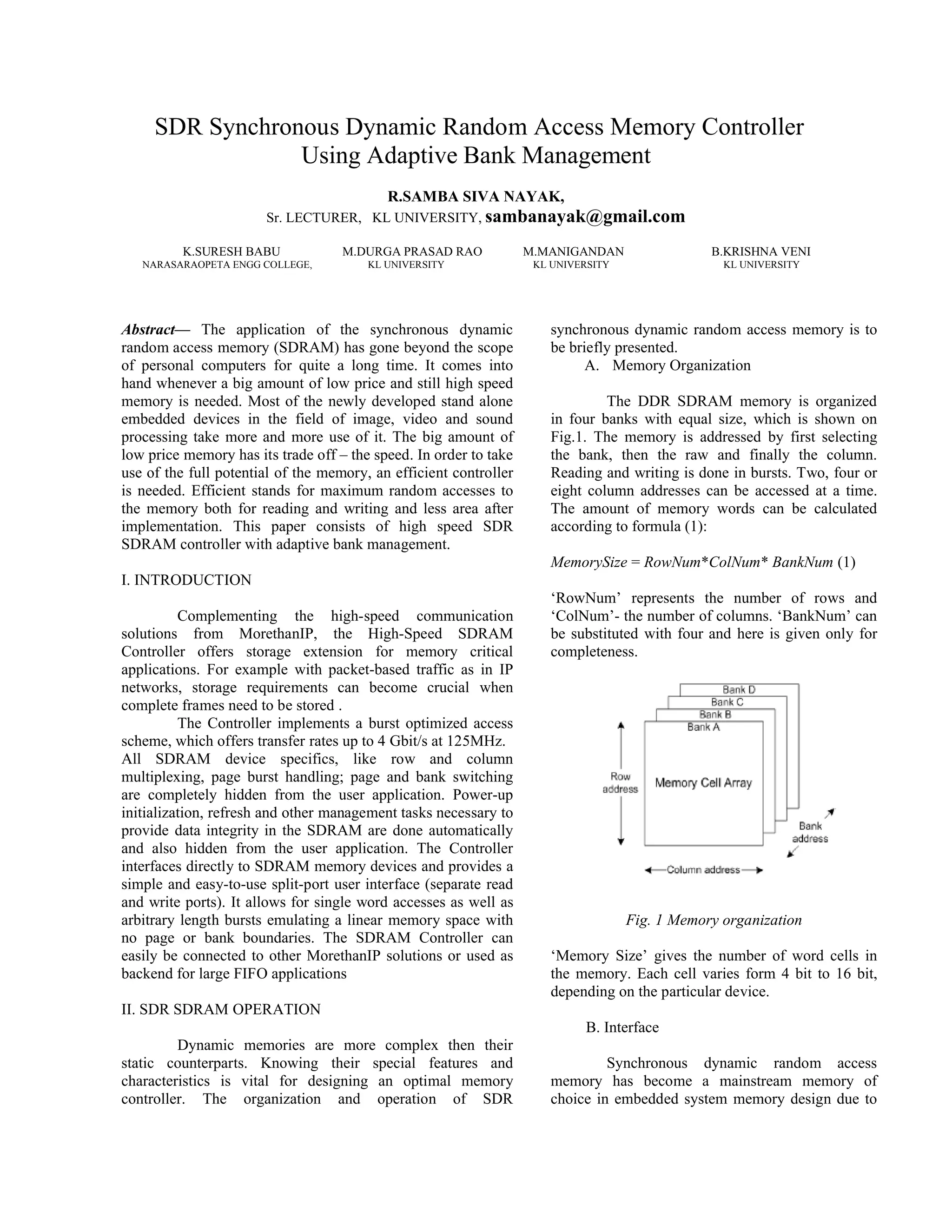
The DDR SDRAM memory is organized
in four banks with equal size, which is shown on
Fig.1. The memory is addressed by first selecting
the bank, then the raw and finally the column.
Reading and writing is done in bursts. Two, four or
eight column addresses can be accessed at a time.
The amount of memory words can be calculated
according to formula (1):
MemorySize = RowNum*ColNum* BankNum (1)
‘RowNum’ represents the number of rows and
‘ColNum’- the number of columns. ‘BankNum’ can
be substituted with four and here is given only for
completeness.
Fig. 1 Memory organization
‘Memory Size’ gives the number of word cells in
the memory. Each cell varies form 4 bit to 16 bit,
depending on the particular device.
B. Interface
Synchronous dynamic random access
memory has become a mainstream memory of
choice in embedded system memory design due to
its speed, burst access and pipeline features. For high-end
applications using processors such as Motorola MPC 8260 or
Intel StrongArm, the interface to the Synchronous dynamic
random access memory is supported by the processor’s built-
in peripheral module. However, for other applications, the
system designer must design a controller to provide proper
commands for dynamic random access memory initialization,
read/write accesses and memory refresh. In some cases,
Synchronous dynamic random access memory is chosen
because the previous generations of dynamic random access
memory (FP and EDO) are either end-of-life or not
recommended for new designs by the memory vendors. From
the board design point of view, design using earlier
generations of dynamic random access memory is much easier
and more straightforward than using SDRAM unless the
system bus master provides the SDRAM interface module as
mentioned above. This SDRAM controller reference design,
located between the SDRAM and the bus master, reduces the
user’s effort to deal with the SDRAM command interface by
providing a simple generic system interface to the bus master.
Figure 2 shows the relationship of the controller between the
bus master and SDRAM. The bus master can be either a
microprocessor or a user’s proprietary module interface.
Fig.2 SDR SDRAM Controller interface
Features:
• Simplifies SDRAM command interface to standard system
read/write interface.
• Internal state machine built for SDRAM power-on
initialization.
• Read/write cycle access time optimized automatically
according to the SDRAM timing spec and the mode it’s
configured to.
• Dedicated auto-refresh request input and acknowledge
output for SDRAM refresh.
• Easily configurable to support different CAS latency and
burst length.
C. Functional description
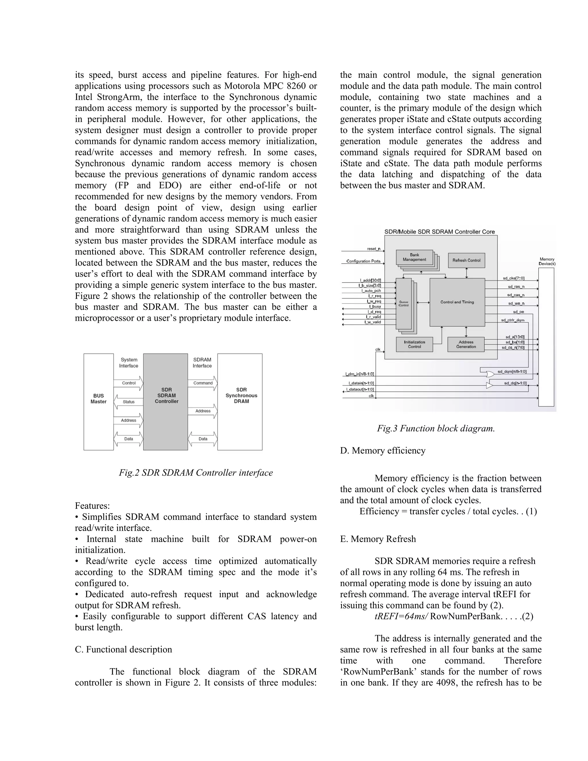
The functional block diagram of the SDRAM
controller is shown in Figure 2. It consists of three modules:
the main control module, the signal generation
module and the data path module. The main control
module, containing two state machines and a
counter, is the primary module of the design which
generates proper iState and cState outputs according
to the system interface control signals. The signal
generation module generates the address and
command signals required for SDRAM based on
iState and cState. The data path module performs
the data latching and dispatching of the data
between the bus master and SDRAM.
Fig.3 Function block diagram.
D. Memory efficiency
Memory efficiency is the fraction between
the amount of clock cycles when data is transferred
and the total amount of clock cycles.
Efficiency = transfer cycles / total cycles. . (1)
E. Memory Refresh
SDR SDRAM memories require a refresh
of all rows in any rolling 64 ms. The refresh in
normal operating mode is done by issuing an auto
refresh command. The average interval tREFI for
issuing this command can be found by (2).
tREFI=64ms/ RowNumPerBank. . . . .(2)
The address is internally generated and the
same row is refreshed in all four banks at the same
time with one command. Therefore
‘RowNumPerBank’ stands for the number of rows
in one bank. If they are 4098, the refresh has to be
done every 15.6 ms. Up to eight auto refresh commands can
be issued one after another and the time interval to the next
refresh command will be extended accordingly.
F. Command Timings
The bank must be opened (activated) for access with an
ACTIVE command; The ACTIVE command selects the bank
and the row to be accessed. Only one row of the given bank
can be activated at same time.The bank must be closed with
the PRECHARGE command and activated again to change the
row in the given bank.All banks must be closed before
automatic refresh. One PRECHARGE command can be used
to close all active banks. Automatic refresh is performed with
an AUTO REFRESH command. READ and WRITE commands
are used to read (or write) burst data. Data access is started at
a selected location and continues for a programmed Burst
Length. The address bits in the READ or WRITE command are
used to select the bank and starting column for the burst
access. Minimal time intervals between all these commands
are limited with SDRAM timings.
Timings t,ns t/clk Tck
Trcd- ACTIVE to read or write delay 18 2.4 3
Trans- ACTIVE to PRECHARGE command42 5.6 6
Twr- Write recovery time 12 1.6 2
Trp- PRECHARGE command period 18 2.4 3
Trrd- ACTIVE bank A to ACTIVE bank B command12 1.6 2
Trfrc- AUTO REFRESH period 60 8 8
Table.1 SDRAM timings for frequency 133MHz
G. Implementation
Non-adaptive controller opens and closes banks for
each transaction. SDRAM command time sequence for two
sequential blocks writing to the same bank and same row will
look like:
1 2 3 4 5 6 7 8 9 10 11
a0 a1 a2 a3 Twr
act a nop nop write a nop nop nop nop pre a nop nop
Tras
Trcd Trp
12 13 14 15 16 17 18 19
a4 a5 a6 a7 Twr
act a nop nop write a nop nop nop nop
Trcd
These two write transactions will consume 19 clock ticks.
Adaptive bank management keeps all banks open and
closes them only to change row or for memory refresh and
SDRAM command sequence for two sequential block writing
will be:
1 2 3 4 5 6 7 8 9 10 11
a0 a1 a2 a3 a4 a5 a6 a7
act a nop nop write a nop nop nop write anop nop nop
These two write transaction will consume
11 clock ticks. It gives a benefit of 8 clock ticks or
42 % of memory writes bandwidth.
This bank access algorithm is called here
as “Adaptive SDRAM bank control“.
IV. Results
All the implementation tests and
simulations are done on Altera Stratix II FPGA
device with following parameters: 24,176 ALMs
(adaptive logic modules), 48,352 ALUTs, 60,440
equivalent LEs, 2,544,192 total memory bits, 36
DSP blocks and 12 PLLs.
Measurement settings:
 measurement cycle duration: 200us
 memory refresh interval is 95% of refresh
period in 15.625μs by default
 addition bus turnaround cycle is used
 transaction burst length is 1,2,4,8,16
 optimal address alignment is used
 Controller clock frequency is 133MHz
 Cas Latency is 3
V. Conclusion
This paper aims to present to the HDL
developing public a non commercial SDR SDRAM
controller, with structure proven to be efficient.
Additionally an address reordering mechanism was
introduced, which saves a lot of clock cycles on the
price of comparatively less extra area.
REFERENCES
[1] Single data Rate (SDR) SDRAM Specification,
JEDEC STANDARD, JESD79E, May 2005
[2] The Love/Hate Relationship with SDR SDRAM
Controllers, Graham Allan, MOSAID, www.design-
reuse.com.
[3] 128Mb SDR SDRAM, Device Specification,
Hynix, April 2006
[4] altdq & altdqs Megafunction, User Guide,
Altera, March 2005
[5] PLLs in Stratix II & Stratix II GX Devices,
April 2006
[6] How to Use SDR SDRAM, User’s Manual,
Document No. E0234E40, ALPIDA, September
2005
[7] SDR SDRAM Controller Using Virtex-4 FPGA
Devices, Oliver Despaux, Application Note, March
27, 2006.

Adaptive bank management[1]

  • 1.
    SDR Synchronous DynamicRandom Access Memory Controller Using Adaptive Bank Management R.SAMBA SIVA NAYAK, Sr. LECTURER, KL UNIVERSITY, sambanayak@gmail.com K.SURESH BABU M.DURGA PRASAD RAO M.MANIGANDAN B.KRISHNA VENI NARASARAOPETA ENGG COLLEGE, KL UNIVERSITY KL UNIVERSITY KL UNIVERSITY Abstract— The application of the synchronous dynamic random access memory (SDRAM) has gone beyond the scope of personal computers for quite a long time. It comes into hand whenever a big amount of low price and still high speed memory is needed. Most of the newly developed stand alone embedded devices in the field of image, video and sound processing take more and more use of it. The big amount of low price memory has its trade off – the speed. In order to take use of the full potential of the memory, an efficient controller is needed. Efficient stands for maximum random accesses to the memory both for reading and writing and less area after implementation. This paper consists of high speed SDR SDRAM controller with adaptive bank management. I. INTRODUCTION Complementing the high-speed communication solutions from MorethanIP, the High-Speed SDRAM Controller offers storage extension for memory critical applications. For example with packet-based traffic as in IP networks, storage requirements can become crucial when complete frames need to be stored . The Controller implements a burst optimized access scheme, which offers transfer rates up to 4 Gbit/s at 125MHz. All SDRAM device specifics, like row and column multiplexing, page burst handling; page and bank switching are completely hidden from the user application. Power-up initialization, refresh and other management tasks necessary to provide data integrity in the SDRAM are done automatically and also hidden from the user application. The Controller interfaces directly to SDRAM memory devices and provides a simple and easy-to-use split-port user interface (separate read and write ports). It allows for single word accesses as well as arbitrary length bursts emulating a linear memory space with no page or bank boundaries. The SDRAM Controller can easily be connected to other MorethanIP solutions or used as backend for large FIFO applications II. SDR SDRAM OPERATION Dynamic memories are more complex then their static counterparts. Knowing their special features and characteristics is vital for designing an optimal memory controller. The organization and operation of SDR synchronous dynamic random access memory is to be briefly presented. A. Memory Organization The DDR SDRAM memory is organized in four banks with equal size, which is shown on Fig.1. The memory is addressed by first selecting the bank, then the raw and finally the column. Reading and writing is done in bursts. Two, four or eight column addresses can be accessed at a time. The amount of memory words can be calculated according to formula (1): MemorySize = RowNum*ColNum* BankNum (1) ‘RowNum’ represents the number of rows and ‘ColNum’- the number of columns. ‘BankNum’ can be substituted with four and here is given only for completeness. Fig. 1 Memory organization ‘Memory Size’ gives the number of word cells in the memory. Each cell varies form 4 bit to 16 bit, depending on the particular device. B. Interface Synchronous dynamic random access memory has become a mainstream memory of choice in embedded system memory design due to
  • 2.
    its speed, burstaccess and pipeline features. For high-end applications using processors such as Motorola MPC 8260 or Intel StrongArm, the interface to the Synchronous dynamic random access memory is supported by the processor’s built- in peripheral module. However, for other applications, the system designer must design a controller to provide proper commands for dynamic random access memory initialization, read/write accesses and memory refresh. In some cases, Synchronous dynamic random access memory is chosen because the previous generations of dynamic random access memory (FP and EDO) are either end-of-life or not recommended for new designs by the memory vendors. From the board design point of view, design using earlier generations of dynamic random access memory is much easier and more straightforward than using SDRAM unless the system bus master provides the SDRAM interface module as mentioned above. This SDRAM controller reference design, located between the SDRAM and the bus master, reduces the user’s effort to deal with the SDRAM command interface by providing a simple generic system interface to the bus master. Figure 2 shows the relationship of the controller between the bus master and SDRAM. The bus master can be either a microprocessor or a user’s proprietary module interface. Fig.2 SDR SDRAM Controller interface Features: • Simplifies SDRAM command interface to standard system read/write interface. • Internal state machine built for SDRAM power-on initialization. • Read/write cycle access time optimized automatically according to the SDRAM timing spec and the mode it’s configured to. • Dedicated auto-refresh request input and acknowledge output for SDRAM refresh. • Easily configurable to support different CAS latency and burst length. C. Functional description The functional block diagram of the SDRAM controller is shown in Figure 2. It consists of three modules: the main control module, the signal generation module and the data path module. The main control module, containing two state machines and a counter, is the primary module of the design which generates proper iState and cState outputs according to the system interface control signals. The signal generation module generates the address and command signals required for SDRAM based on iState and cState. The data path module performs the data latching and dispatching of the data between the bus master and SDRAM. Fig.3 Function block diagram. D. Memory efficiency Memory efficiency is the fraction between the amount of clock cycles when data is transferred and the total amount of clock cycles. Efficiency = transfer cycles / total cycles. . (1) E. Memory Refresh SDR SDRAM memories require a refresh of all rows in any rolling 64 ms. The refresh in normal operating mode is done by issuing an auto refresh command. The average interval tREFI for issuing this command can be found by (2). tREFI=64ms/ RowNumPerBank. . . . .(2) The address is internally generated and the same row is refreshed in all four banks at the same time with one command. Therefore ‘RowNumPerBank’ stands for the number of rows in one bank. If they are 4098, the refresh has to be
  • 3.
    done every 15.6ms. Up to eight auto refresh commands can be issued one after another and the time interval to the next refresh command will be extended accordingly. F. Command Timings The bank must be opened (activated) for access with an ACTIVE command; The ACTIVE command selects the bank and the row to be accessed. Only one row of the given bank can be activated at same time.The bank must be closed with the PRECHARGE command and activated again to change the row in the given bank.All banks must be closed before automatic refresh. One PRECHARGE command can be used to close all active banks. Automatic refresh is performed with an AUTO REFRESH command. READ and WRITE commands are used to read (or write) burst data. Data access is started at a selected location and continues for a programmed Burst Length. The address bits in the READ or WRITE command are used to select the bank and starting column for the burst access. Minimal time intervals between all these commands are limited with SDRAM timings. Timings t,ns t/clk Tck Trcd- ACTIVE to read or write delay 18 2.4 3 Trans- ACTIVE to PRECHARGE command42 5.6 6 Twr- Write recovery time 12 1.6 2 Trp- PRECHARGE command period 18 2.4 3 Trrd- ACTIVE bank A to ACTIVE bank B command12 1.6 2 Trfrc- AUTO REFRESH period 60 8 8 Table.1 SDRAM timings for frequency 133MHz G. Implementation Non-adaptive controller opens and closes banks for each transaction. SDRAM command time sequence for two sequential blocks writing to the same bank and same row will look like: 1 2 3 4 5 6 7 8 9 10 11 a0 a1 a2 a3 Twr act a nop nop write a nop nop nop nop pre a nop nop Tras Trcd Trp 12 13 14 15 16 17 18 19 a4 a5 a6 a7 Twr act a nop nop write a nop nop nop nop Trcd These two write transactions will consume 19 clock ticks. Adaptive bank management keeps all banks open and closes them only to change row or for memory refresh and SDRAM command sequence for two sequential block writing will be: 1 2 3 4 5 6 7 8 9 10 11 a0 a1 a2 a3 a4 a5 a6 a7 act a nop nop write a nop nop nop write anop nop nop These two write transaction will consume 11 clock ticks. It gives a benefit of 8 clock ticks or 42 % of memory writes bandwidth. This bank access algorithm is called here as “Adaptive SDRAM bank control“. IV. Results All the implementation tests and simulations are done on Altera Stratix II FPGA device with following parameters: 24,176 ALMs (adaptive logic modules), 48,352 ALUTs, 60,440 equivalent LEs, 2,544,192 total memory bits, 36 DSP blocks and 12 PLLs. Measurement settings:  measurement cycle duration: 200us  memory refresh interval is 95% of refresh period in 15.625μs by default  addition bus turnaround cycle is used  transaction burst length is 1,2,4,8,16  optimal address alignment is used  Controller clock frequency is 133MHz  Cas Latency is 3 V. Conclusion This paper aims to present to the HDL developing public a non commercial SDR SDRAM controller, with structure proven to be efficient. Additionally an address reordering mechanism was introduced, which saves a lot of clock cycles on the price of comparatively less extra area. REFERENCES [1] Single data Rate (SDR) SDRAM Specification, JEDEC STANDARD, JESD79E, May 2005 [2] The Love/Hate Relationship with SDR SDRAM Controllers, Graham Allan, MOSAID, www.design- reuse.com. [3] 128Mb SDR SDRAM, Device Specification, Hynix, April 2006 [4] altdq & altdqs Megafunction, User Guide, Altera, March 2005 [5] PLLs in Stratix II & Stratix II GX Devices, April 2006 [6] How to Use SDR SDRAM, User’s Manual, Document No. E0234E40, ALPIDA, September 2005 [7] SDR SDRAM Controller Using Virtex-4 FPGA Devices, Oliver Despaux, Application Note, March 27, 2006.