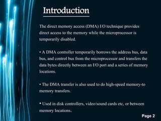
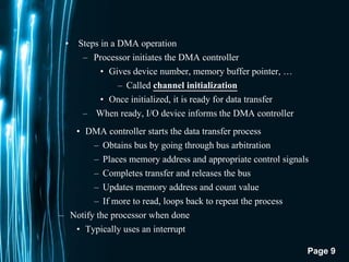
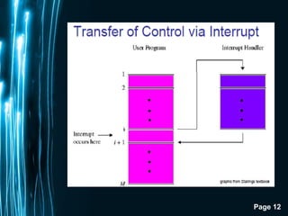
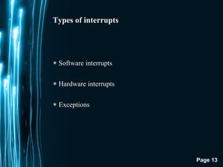
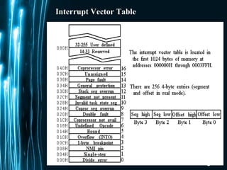
The document discusses direct memory access (DMA) and interrupts. It describes how DMA allows direct data transfer between memory and I/O devices without involving the CPU. This is handled by a DMA controller through a request-grant handshake using HOLD and HLDA pins. The document also categorizes different types of interrupts like hardware, software and exceptions. It explains how interrupts alter program flow and are serviced by interrupt service routines (ISRs) through an interrupt vector table.

![Page 22
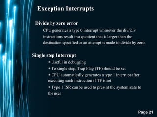
Exception Interrupts
There exists no instruction to directly set or reset trap flag.
TF=1 can be set by executing the following sequence of instructions:
PUSHF
MOV BP,SP
OR WORD PTR[BP+0],0100H
POPF
TF=0 can be set by executing the following sequence of instructions:
PUSHF
MOV BP,SP
AND WORD PTR[BP+0],0FEFFH
POPF](https://image.slidesharecdn.com/dmainterrupts-180202064240/85/Direct-Memory-Access-Interrrupts-22-320.jpg)


![DMA presentation [By- Digvijay]](https://cdn.slidesharecdn.com/ss_thumbnails/digvijay-dmapresentation-131231041837-phpapp02-thumbnail.jpg?width=640&height=640&fit=bounds)


![[Deck] What's New in Spark-Iceberg Integration via DSV2.pptx](https://cdn.slidesharecdn.com/ss_thumbnails/deckwhatsnewinspark-icebergintegrationviadsv2-260210005337-25955b12-thumbnail.jpg?width=640&height=640&fit=bounds)