UCSD - ECE 260A: VLSI DESIGN PROJECT
Page 1 of 9 ECE 260A PROJECT – Fall 2015
Design and Simulation of an 8-Bit Processor and Its
Associated 32-Byte SRAM
Fanyu Yang, A53102865
Haoran Pu, A53104427
1. Design Challenge and Significance
Microprocessor design takes entry-level engineering students through
a decently complicated circuit design process which involve static
circuit, dynamic circuit, sequential logic, combinational logic, and
memory arrays, etc. The microprocessor design process requires a
comprehensive and integral understanding of the entire
microprocessor as well as precise and efficient operation of every
single subsystem, such as SRAM, register file. The microprocessor
consists of five major subsystems: register file, control logic unit,
arithmetic logic unit (ALU), SRAM, and program counter.
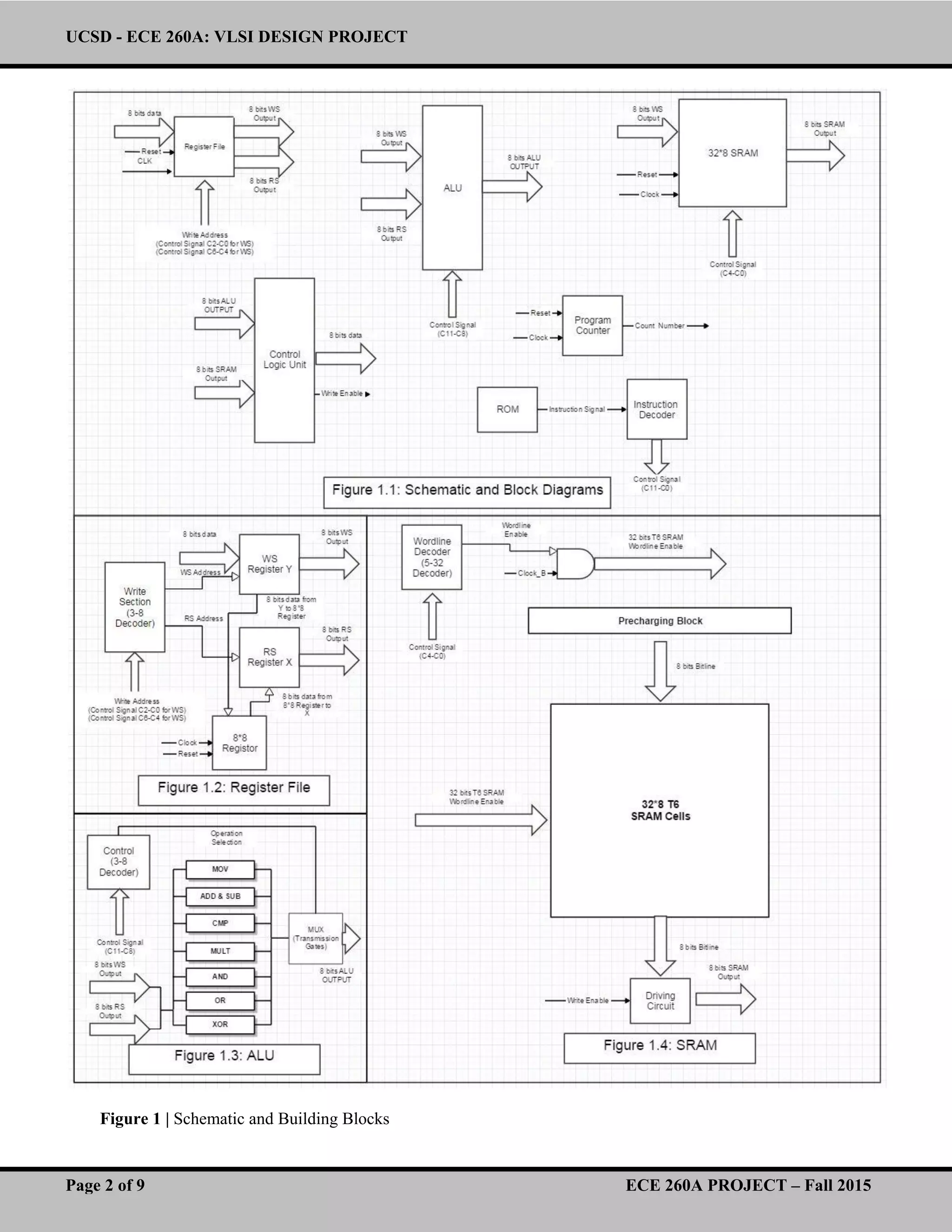
The register file block (see Figure 1.2) is used to store operating
numbers. The key challenge is how to block unselected registers when
data is written into selected registers or when selected registers send
data out in reading operation. 64 8-1 multiplexers can be used to block
unselected registers at the expense of larger power consumption.
Instead of multiplexers, transmission gates implement the same
function with low power consumption, but the output of the
transmission gates become floating points when the gates switch off,
which causes serious problem. An alternative energy efficient way to
block unselected registers is to use transmission gates with certain
optimization. A pull down network is inserted at the output of the
transmission gates to pull the outputs down to the ground when
complementary enable signal is inserted.
For the control logic unit, it is vital to send correct control signals to
the corresponding systems and this operation involves plenty of
accurate bus notations.
ALU block (see Figure 1.3) works as a calculator to implement
arithmetic operations, such as addition, subtraction, and
multiplication. The major challenge is to turn off unwanted operations
in ALU. The solution is using transmission gates to select required
calculation results. Enable signals generated by the 4-16 decoder are
used to turn on the transmission gate for the required operation and
turn off the gates of unselected operations. By turning of the
unselected arithmetic sub-block, power consumption of the ALU
decreases significantly and operating speed increases.
SRAM (see Figure 1.4) works as a memory element in the
microprocessor. In the SRAM design, 256 6T SRAM cells are used.
6T SRAM cell require ratio logic. The primary challenge for SRAM is
sizing of transistors, which has considerable influence on operating
speed, power consumption, and even the validity and correctness of
the result.
Program counter is used to count the number of operations executed
after inserting a reset signal. The major challenge is caused by reset
signals. Since the reset operation of the D flip-flops is synchronous,
which means reset insertion happens at the rising edge of the clock, if
the output of the last D flip-flop, namely Q, feeds into the clock of the
next D flip-flop, the reset of the next D flip-flop can have a delay
compared with the next D flip-flop, which causes severe problem. By
adding 5 half-adder, two D flip-flops can reset at the same time and
this problem is solved.
2. Architecture Description
The microprocessor (see Figure 1.1) has five building blocks in which
three of them are very important – register file, ALU, and SRAM.
Register file block (see Figure 1.2) is used to write and read data using
its address. The 3-8 decoder generates address for WS (write
selection) and RS (read selection) blocks. Data feeds into WS to write
the data in the address decoded by the decoder and then the data go
into the 8*8 register from WS. In the next operation cycle, the stored
data feeds to RS from the 8*8 register and then export as an 8 bits
output data from RS. 8 bits output data can also export directly from
WS.
ALU (see Figure 1.3) is the major part carrying out arithmetic
operations. Control signals feeding into the 3-8 decoder generate
operation selection signals, which feed into the multiplexer to choose
one of eight arithmetic operations. 8 bits output from WS register Y
and 8 bits output from RS register X are sent as inputs to the
arithmetic operation blocks, however only selected operation can
execute. The 8 bits output of ALU are sent back to the control logic
unit waiting for next cycle operation.
SRAM (see Figure 1.4) is used to store data which is not being current
used. Control signals are fed into a 5-32 decoder to generate 32 bits
wordline enable signals. Since wordline should not be enabled if T6
SRAM cells are in precharging stage, an AND operation between
complementary clock signal and wordline enable signals should be
added before wordline enable signals turn SRAM cells on. For writing
operation, Write Enable inserted, 8 bits input data are written into
SRAM cells through bitlines. For reading operation, data in SRAM
cells are sent out to 8 bits SRAM output and then fed back to control
logic unit.
3. Innovation
Transmission gate logic is applied to almost all multiplexers to
increase speed and reduce power consumption. In register file block,
transmission gates are used to select required registers and block other
registers. In ALU block, transmission gate controls which arithmetic
operation is carry out.
4. Remaining Problem
The major problem is that reading 8 bits output from register X has
some delay from the rising edge of the clock witch result in reading 8
bits output from register Y happens at the next rising edge of the
clock. This happens when ALU has large delay. Reducing ALU delay
can eliminate that miss match.
5. Future Iterations
The microprocessor design can be improved by using 10T SRAM
instead of 6T SRAM.
References:
[1] Weste, H. (2011). CMOS VLSI Design – A Circuits and Systems
Perspective. 4th
Edition.
UCSD - ECE 260A: VLSI DESIGN PROJECT
Page 2 of 9 ECE 260A PROJECT – Fall 2015
Figure 1 | Schematic and Building Blocks
UCSD - ECE 260A: VLSI DESIGN PROJECT
Page 3 of 9 ECE 260A PROJECT – Fall 2015
Figure 2 | Schematic of Multiplier
Z<0:7>
A<0:3>
B<0:3>
GND
VDD
A<3>
A<3>
A<3>
A<2>
A<3> A<2>
A<2>
A<2> A<1>
A<1>
A<1>
A<1> A<0>
A<0>
A<0>
A<0>
B<0>
Z<0>
B<1>
Z<1>
B<2>
Z<2>
B<3>
FAFAFA
FAFAFA
FAFA HALFHALF
HALF
HALF
UCSD - ECE 260A: VLSI DESIGN PROJECT
Page 4 of 9 ECE 260A PROJECT – Fall 2015
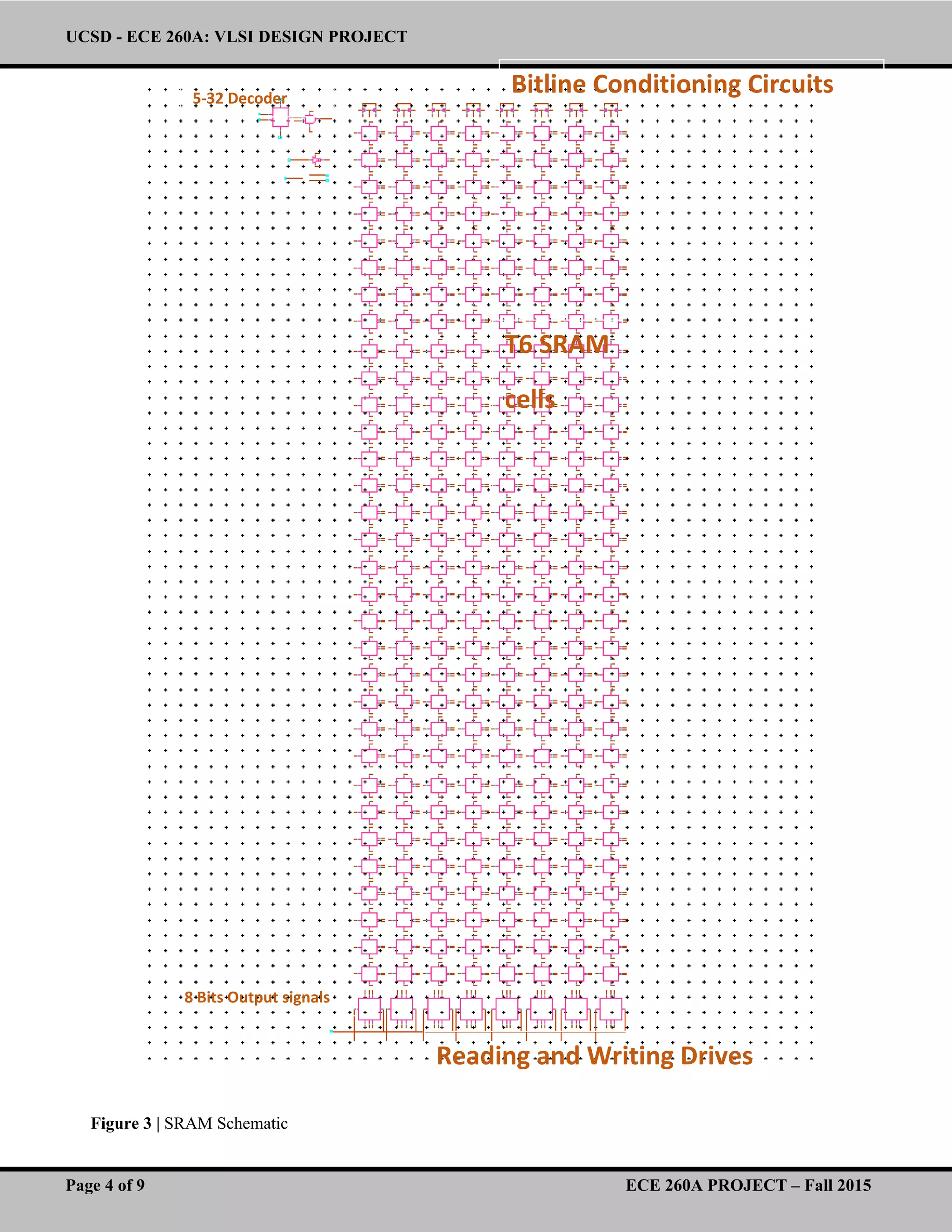
Figure 3 | SRAM Schematic
T6 SRAM
cells
Bitline Conditioning Circuits
Reading and Writing Drives
5-32 Decoder
8 Bits Output signals
UCSD - ECE 260A: VLSI DESIGN PROJECT
Page 5 of 9 ECE 260A PROJECT – Fall 2015
Figure 4 | Schematic of Test Bench
UCSD - ECE 260A: VLSI DESIGN PROJECT
Page 6 of 9 ECE 260A PROJECT – Fall 2015
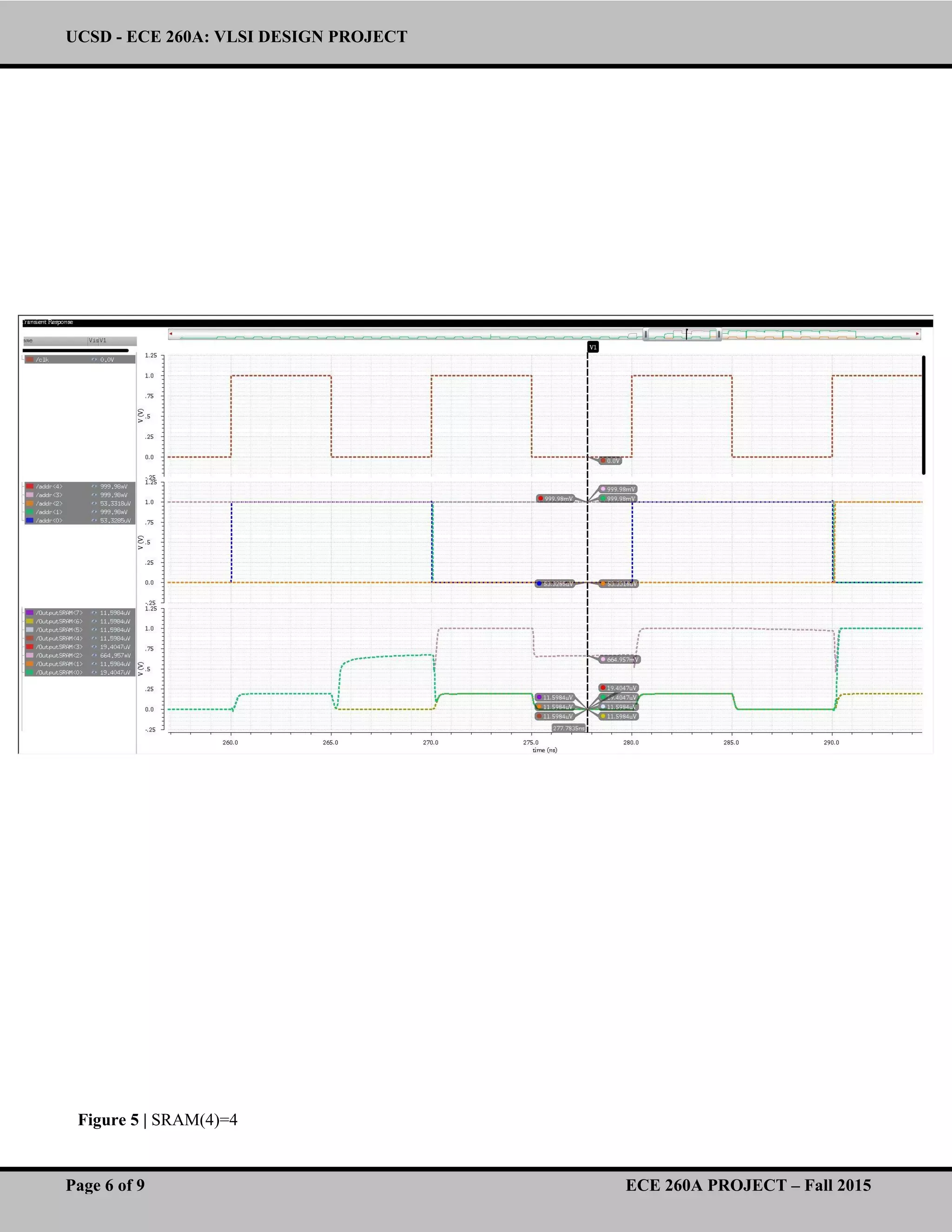
Figure 5 | SRAM(4)=4
UCSD - ECE 260A: VLSI DESIGN PROJECT
Page 7 of 9 ECE 260A PROJECT – Fall 2015
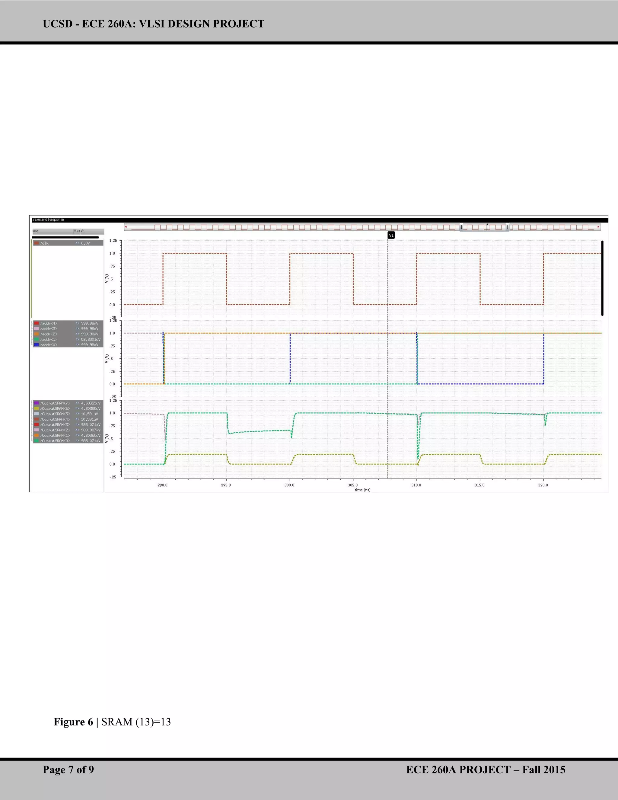
Figure 6 | SRAM (13)=13
UCSD - ECE 260A: VLSI DESIGN PROJECT
Page 8 of 9 ECE 260A PROJECT – Fall 2015
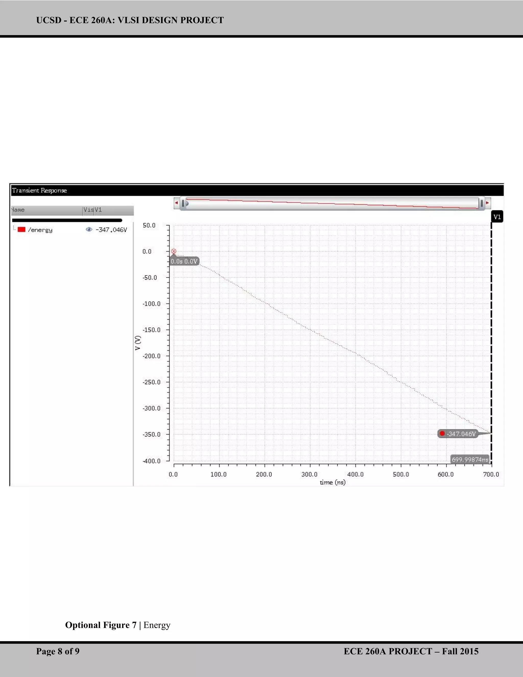
Optional Figure 7 | Energy
UCSD - ECE 260A: VLSI DESIGN PROJECT
Page 9 of 9 ECE 260A PROJECT – Fall 2015
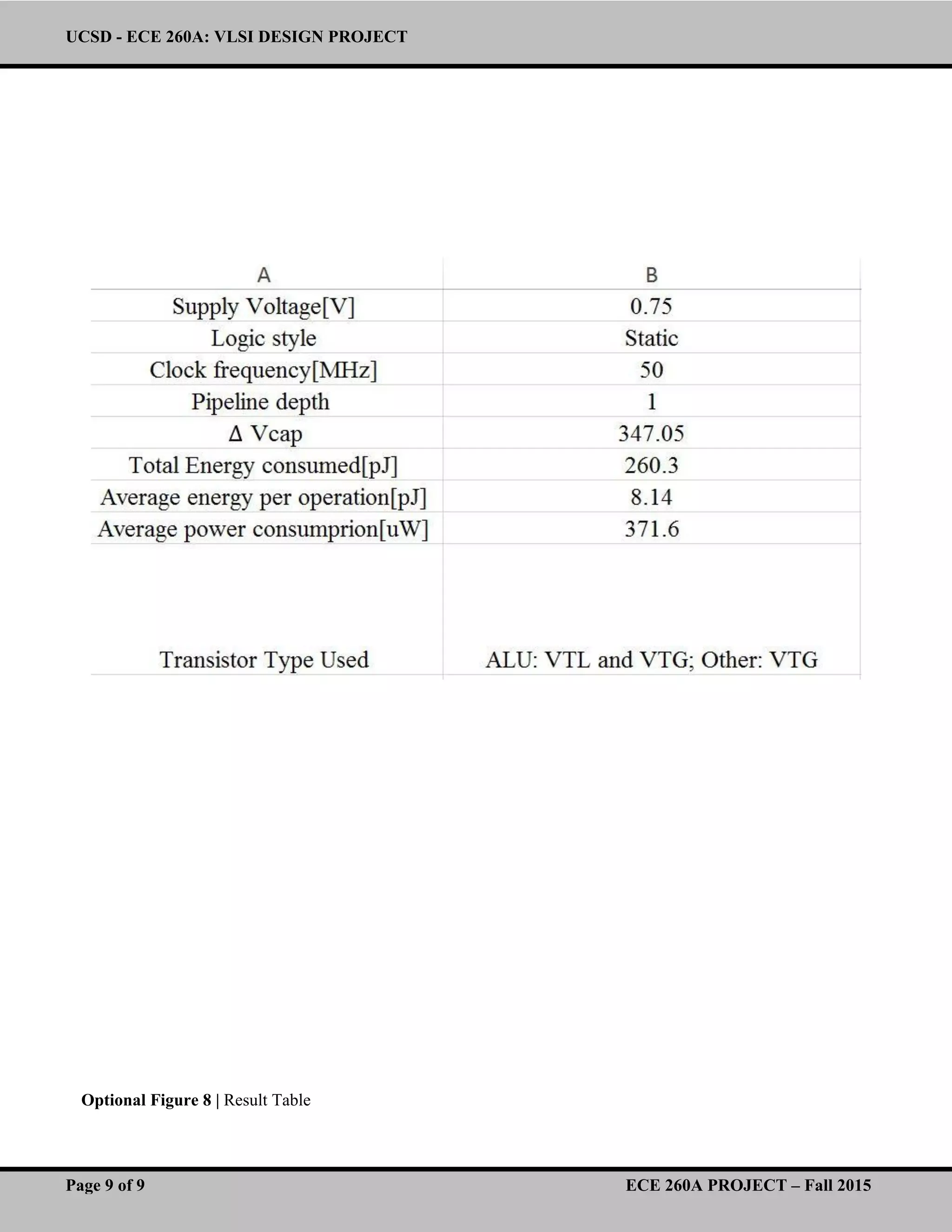
Optional Figure 8 | Result Table

ece260project.doc

  • 1.
    UCSD - ECE260A: VLSI DESIGN PROJECT Page 1 of 9 ECE 260A PROJECT – Fall 2015 Design and Simulation of an 8-Bit Processor and Its Associated 32-Byte SRAM Fanyu Yang, A53102865 Haoran Pu, A53104427 1. Design Challenge and Significance Microprocessor design takes entry-level engineering students through a decently complicated circuit design process which involve static circuit, dynamic circuit, sequential logic, combinational logic, and memory arrays, etc. The microprocessor design process requires a comprehensive and integral understanding of the entire microprocessor as well as precise and efficient operation of every single subsystem, such as SRAM, register file. The microprocessor consists of five major subsystems: register file, control logic unit, arithmetic logic unit (ALU), SRAM, and program counter. The register file block (see Figure 1.2) is used to store operating numbers. The key challenge is how to block unselected registers when data is written into selected registers or when selected registers send data out in reading operation. 64 8-1 multiplexers can be used to block unselected registers at the expense of larger power consumption. Instead of multiplexers, transmission gates implement the same function with low power consumption, but the output of the transmission gates become floating points when the gates switch off, which causes serious problem. An alternative energy efficient way to block unselected registers is to use transmission gates with certain optimization. A pull down network is inserted at the output of the transmission gates to pull the outputs down to the ground when complementary enable signal is inserted. For the control logic unit, it is vital to send correct control signals to the corresponding systems and this operation involves plenty of accurate bus notations. ALU block (see Figure 1.3) works as a calculator to implement arithmetic operations, such as addition, subtraction, and multiplication. The major challenge is to turn off unwanted operations in ALU. The solution is using transmission gates to select required calculation results. Enable signals generated by the 4-16 decoder are used to turn on the transmission gate for the required operation and turn off the gates of unselected operations. By turning of the unselected arithmetic sub-block, power consumption of the ALU decreases significantly and operating speed increases. SRAM (see Figure 1.4) works as a memory element in the microprocessor. In the SRAM design, 256 6T SRAM cells are used. 6T SRAM cell require ratio logic. The primary challenge for SRAM is sizing of transistors, which has considerable influence on operating speed, power consumption, and even the validity and correctness of the result. Program counter is used to count the number of operations executed after inserting a reset signal. The major challenge is caused by reset signals. Since the reset operation of the D flip-flops is synchronous, which means reset insertion happens at the rising edge of the clock, if the output of the last D flip-flop, namely Q, feeds into the clock of the next D flip-flop, the reset of the next D flip-flop can have a delay compared with the next D flip-flop, which causes severe problem. By adding 5 half-adder, two D flip-flops can reset at the same time and this problem is solved. 2. Architecture Description The microprocessor (see Figure 1.1) has five building blocks in which three of them are very important – register file, ALU, and SRAM. Register file block (see Figure 1.2) is used to write and read data using its address. The 3-8 decoder generates address for WS (write selection) and RS (read selection) blocks. Data feeds into WS to write the data in the address decoded by the decoder and then the data go into the 8*8 register from WS. In the next operation cycle, the stored data feeds to RS from the 8*8 register and then export as an 8 bits output data from RS. 8 bits output data can also export directly from WS. ALU (see Figure 1.3) is the major part carrying out arithmetic operations. Control signals feeding into the 3-8 decoder generate operation selection signals, which feed into the multiplexer to choose one of eight arithmetic operations. 8 bits output from WS register Y and 8 bits output from RS register X are sent as inputs to the arithmetic operation blocks, however only selected operation can execute. The 8 bits output of ALU are sent back to the control logic unit waiting for next cycle operation. SRAM (see Figure 1.4) is used to store data which is not being current used. Control signals are fed into a 5-32 decoder to generate 32 bits wordline enable signals. Since wordline should not be enabled if T6 SRAM cells are in precharging stage, an AND operation between complementary clock signal and wordline enable signals should be added before wordline enable signals turn SRAM cells on. For writing operation, Write Enable inserted, 8 bits input data are written into SRAM cells through bitlines. For reading operation, data in SRAM cells are sent out to 8 bits SRAM output and then fed back to control logic unit. 3. Innovation Transmission gate logic is applied to almost all multiplexers to increase speed and reduce power consumption. In register file block, transmission gates are used to select required registers and block other registers. In ALU block, transmission gate controls which arithmetic operation is carry out. 4. Remaining Problem The major problem is that reading 8 bits output from register X has some delay from the rising edge of the clock witch result in reading 8 bits output from register Y happens at the next rising edge of the clock. This happens when ALU has large delay. Reducing ALU delay can eliminate that miss match. 5. Future Iterations The microprocessor design can be improved by using 10T SRAM instead of 6T SRAM. References: [1] Weste, H. (2011). CMOS VLSI Design – A Circuits and Systems Perspective. 4th Edition.
  • 2.
    UCSD - ECE260A: VLSI DESIGN PROJECT Page 2 of 9 ECE 260A PROJECT – Fall 2015 Figure 1 | Schematic and Building Blocks
  • 3.
    UCSD - ECE260A: VLSI DESIGN PROJECT Page 3 of 9 ECE 260A PROJECT – Fall 2015 Figure 2 | Schematic of Multiplier Z<0:7> A<0:3> B<0:3> GND VDD A<3> A<3> A<3> A<2> A<3> A<2> A<2> A<2> A<1> A<1> A<1> A<1> A<0> A<0> A<0> A<0> B<0> Z<0> B<1> Z<1> B<2> Z<2> B<3> FAFAFA FAFAFA FAFA HALFHALF HALF HALF
  • 4.
    UCSD - ECE260A: VLSI DESIGN PROJECT Page 4 of 9 ECE 260A PROJECT – Fall 2015 Figure 3 | SRAM Schematic T6 SRAM cells Bitline Conditioning Circuits Reading and Writing Drives 5-32 Decoder 8 Bits Output signals
  • 5.
    UCSD - ECE260A: VLSI DESIGN PROJECT Page 5 of 9 ECE 260A PROJECT – Fall 2015 Figure 4 | Schematic of Test Bench
  • 6.
    UCSD - ECE260A: VLSI DESIGN PROJECT Page 6 of 9 ECE 260A PROJECT – Fall 2015 Figure 5 | SRAM(4)=4
  • 7.
    UCSD - ECE260A: VLSI DESIGN PROJECT Page 7 of 9 ECE 260A PROJECT – Fall 2015 Figure 6 | SRAM (13)=13
  • 8.
    UCSD - ECE260A: VLSI DESIGN PROJECT Page 8 of 9 ECE 260A PROJECT – Fall 2015 Optional Figure 7 | Energy
  • 9.
    UCSD - ECE260A: VLSI DESIGN PROJECT Page 9 of 9 ECE 260A PROJECT – Fall 2015 Optional Figure 8 | Result Table