Downloaded 37 times
![International Journal of VLSI design & Communication Systems (VLSICS) Vol.4, No.4, August 2013
42
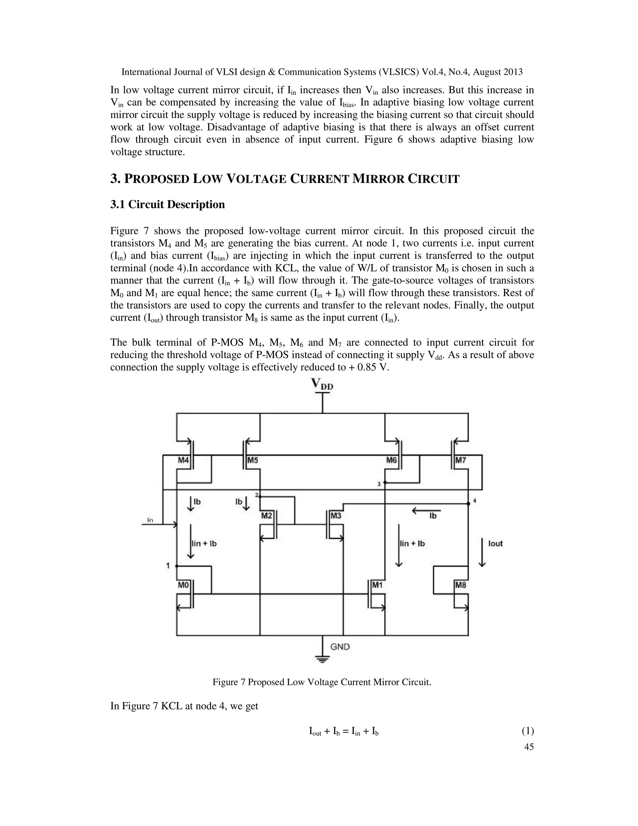
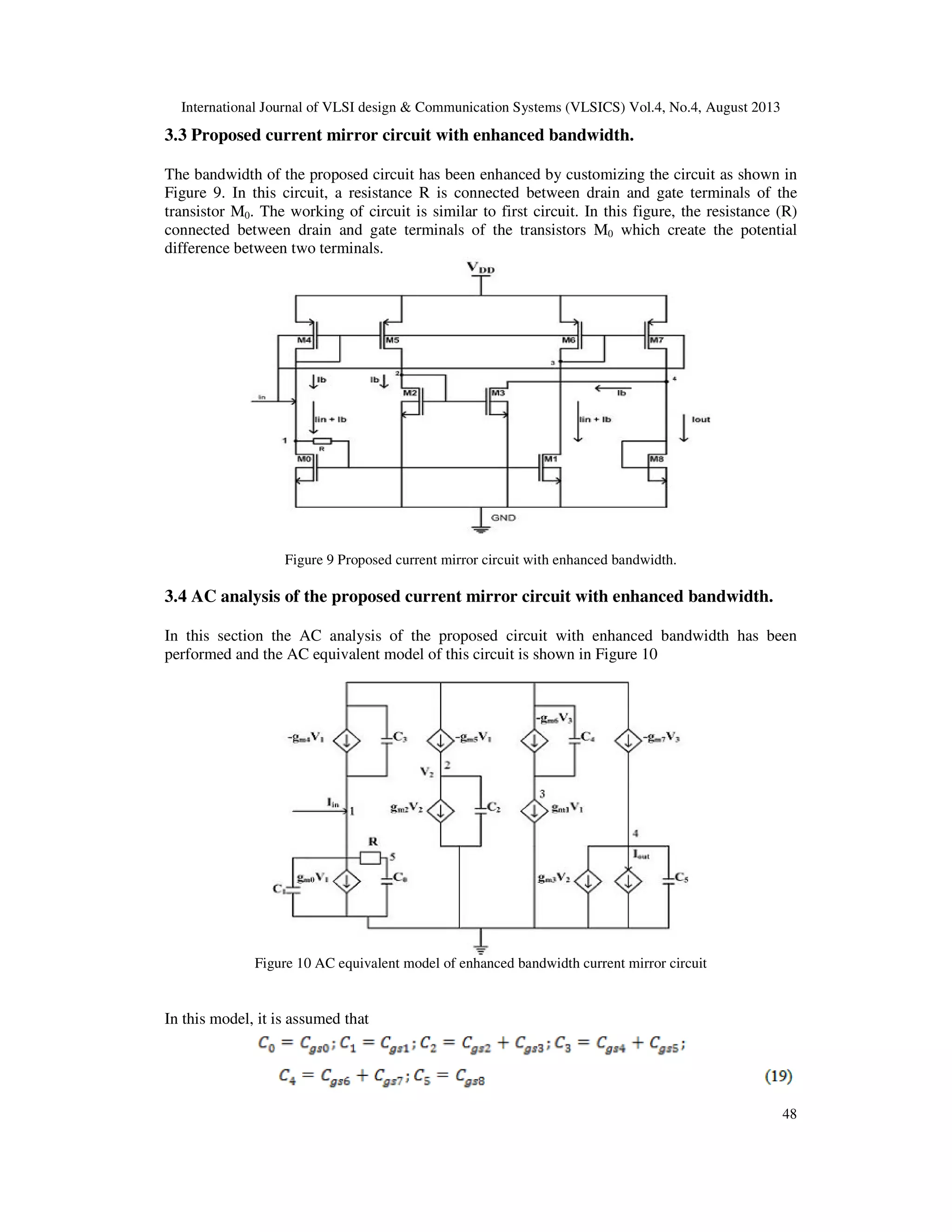
The bulk-driven technique is used to scale down the threshold voltage of PMOS transistor used in
circuit. The body terminal of PMOS is connected to input to provide weak positive bias so that
threshold voltage of PMOS is reduced and supply voltage is effectively scale down. This
technique is completely compatible with standard CMOS process.
Current mirror (CM) circuits are widely used in analog integrated circuit. It is clear from its name
that it copies the current. Current mirror are circuits whose output current is independent of
output terminal voltage and depends on input current only. They are used for current
amplification, biasing, active loading and level shifting. Efficient design of current mirror circuit
improves the overall performance of analog integrated circuit and reduces the supply voltage
requirement of the circuit.
2. PREVIOUSLY REPORTED CURRENT MIRROR CIRCUITS
2.1 Very Low Input impedance Low Power Current Mirror
In order to get low input impedance, the main idea is to introduce transistor M3 in series with the
input terminal of the basic circuit of the current mirror and use a gain amplifier of ‘−A’ gain to
control the gate voltage of M3. In Figure 2 (a) a simple current mirror is shown and in Figure 2 (b)
conceptual schematic of the current mirror. Any increase in source voltage of M3 (i.e. due to
injected input current) causes its gate voltage to decrease ‘−A’ times, hence causing stronger sink
of input current which results in decrease of input impedance by ‘A’ times.
Figure 2 (a) Simple current mirror (b) Conceptual schematic of the current mirror [4].
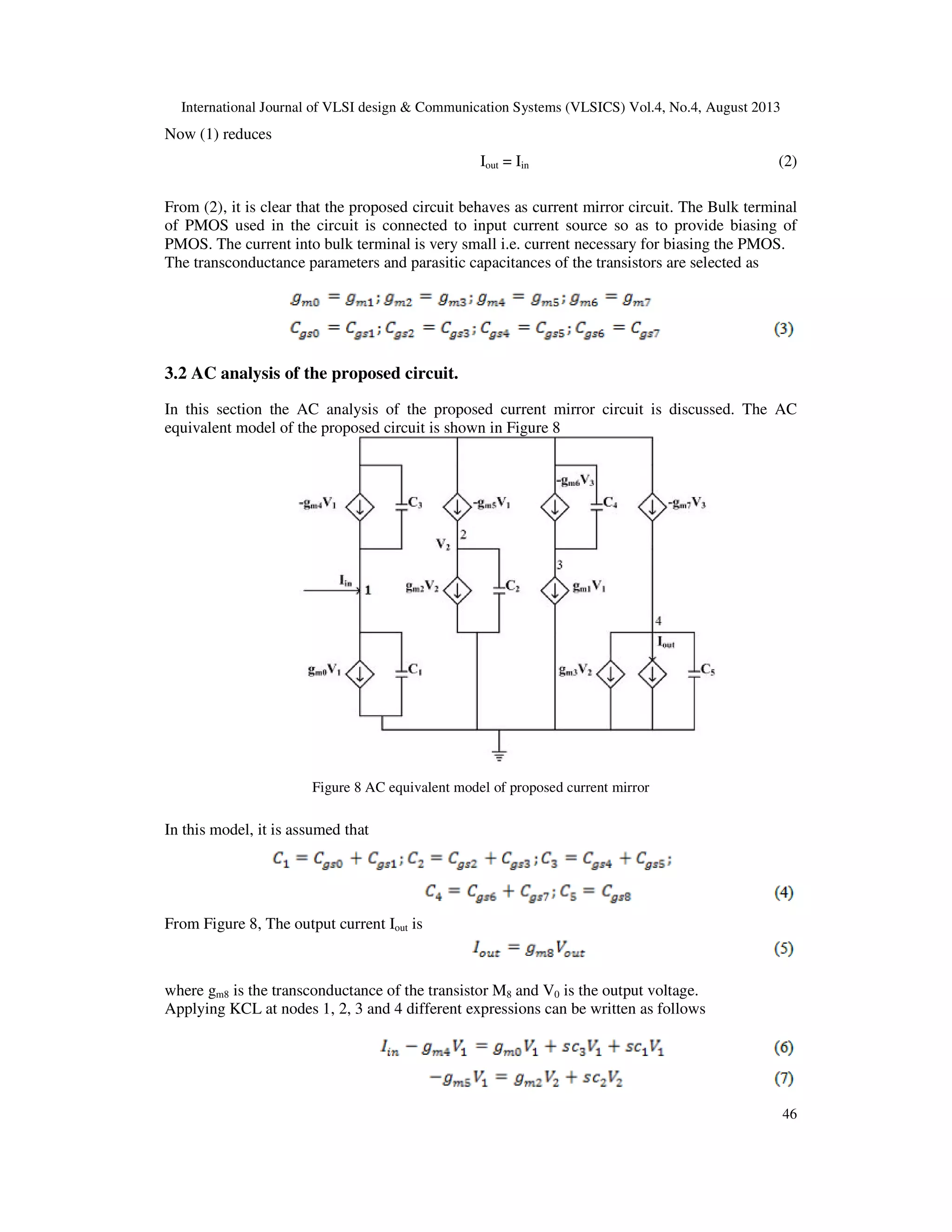
2.2 Self Cascode Current Mirror
As the device sizes are reducing the output impedance of the MOSFET is also reducing due to the
channel length modulation. For having high gains we need high output impedance of the devices
and short channel MOSFETs cannot provide high gain structures for which cascoding of
MOSFETs is the obvious technique. Cascode MOSFETs increase the gains but it decreases the
output signal swing as well. The technique is to use the self cascode structure which requires low
compliance voltages at output nodes as compare to regular cascode and provides high output](https://image.slidesharecdn.com/anewlowvoltagep-mosbulkdrivencurrentmirrorcircuit-130912015109-phpapp01/75/A-NEW-LOW-VOLTAGE-P-MOS-BULK-DRIVEN-CURRENT-MIRROR-CIRCUIT-2-2048.jpg)
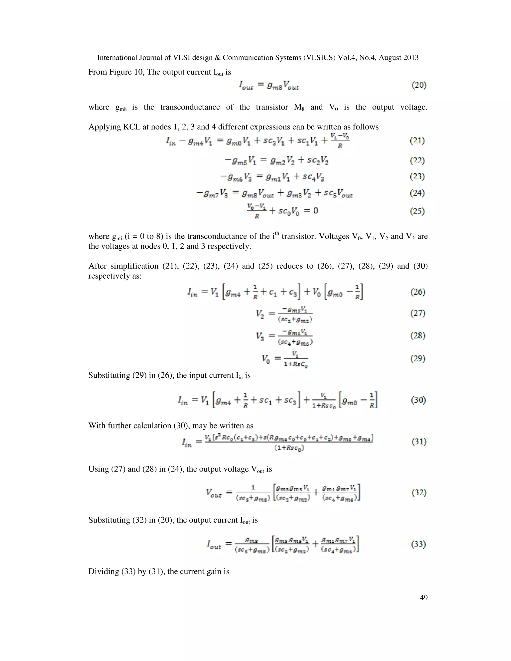
![International Journal of VLSI design & Communication Systems (VLSICS) Vol.4, No.4, August 2013
43
impedance to give high output gains. This approach has potential applications in low voltage
design.
A self-cascode is a 2-transistor structure which can easily be treated as a single composite
transistor. The composite structure has higher effective channel length and the effective output
conductance is much low. The lower transistor M1 is equivalent to a resistor, where value is input
dependant. For optimal operation, the W/L ratio of M2 must be greater than that of M1, i.e., m>l.
For the composite transistor, the effective trans-conductance is given as
Figure 4 Self Cascode Current mirror [6].
2.3 Multi Input Floating Gate Low Voltage Current Mirror
The Current Mirrors are basic elements for the design of low voltage circuits and many low
voltage current mirror circuits have been developed. Most of these circuits have low compliance
voltage at output node but many of them have high compliance voltage at the input node. There
are few circuits only which have low input and output compliance voltages. However they have
high offset current, thus limiting operating range. To increase their operating range, a technique
named as multiple inputs floating gate (MIFG) need to be examined.
In multi input floating gate current mirror circuit the threshold voltage of MOSFET is made
programmable with input current Iin .This can done by providing feedback of Iin which produce a
voltage proportional to the Iin. This is done by passing Iin through a resistor. The voltage drop is
high for high Iin while it will be low at low Iin. Hence the threshold voltage of the circuit is varied
in accordance with the requirement of the circuit.](https://image.slidesharecdn.com/anewlowvoltagep-mosbulkdrivencurrentmirrorcircuit-130912015109-phpapp01/75/A-NEW-LOW-VOLTAGE-P-MOS-BULK-DRIVEN-CURRENT-MIRROR-CIRCUIT-3-2048.jpg)
![International Journal of VLSI design & Communication Systems (VLSICS) Vol.4, No.4, August 2013
44
Figure 5 Multi input floating gate Current mirror [7].
In Figure 5, the threshold voltage of M1 is varied as per requirement of the circuit. For low value
of Iin threshold value is reduced and when Iin is high threshold voltage increases as per
requirement of the circuit.
2.4 Adaptive Biasing Low voltage current mirror
Figure 6 Adaptive biasing Current mirror structure [8].](https://image.slidesharecdn.com/anewlowvoltagep-mosbulkdrivencurrentmirrorcircuit-130912015109-phpapp01/75/A-NEW-LOW-VOLTAGE-P-MOS-BULK-DRIVEN-CURRENT-MIRROR-CIRCUIT-4-2048.jpg)

![International Journal of VLSI design & Communication Systems (VLSICS) Vol.4, No.4, August 2013
52
TABLE 2 Comparison of proposed current mirror with other reported current mirror.
Circuit Parameters Current mirror [4] Current mirror [1] Proposed current mirror
Power supply +1.5 V +1.3 V +0.85 V
CMOS Technology 180 nm 180nm 180nm
Input Current Range 0 to 100uA 0 to 100uA 0 to 100uA
Bandwidth 577MHz 163MHz 92MHz
5. CONCLUSION
This work presents a new low voltage current mirror circuit operating with a supply voltage of
+0.85 V. The proposed circuit can be used for wide variety of low voltage and low power
application. The bandwidth of the circuit has been enhanced using resistive compensation
technique. The mathematical analysis of the proposed low voltage current mirror has also been
presented.The simulation results have been presented to validate the usefulness of the proposed
current mirror circuit.
ACKNOWLEDGEMENTS
First of all, i am thankful to mrs. laxmi kumre, assistant professor, electronics and communication
engineering department, maulana azad national institute of technology, bhopal for his patient
guidance and support throughout this work.
I am thankful to entire faculty and staff electronics and communication engineering department.
Finally, i would like to thank my family and friends for standing by me through all the joys and
sorrows that life had to offer.
REFERENCES
[1] Manish Tikyani and Rishikesh pandey, “A New Low-Voltage Current Mirror Circuit with Enhanced
Bandwidth”, International Conference on Computational Intelligence and Communication Networks,
pp 42-46, Oct 2011.
[2] Naresh Lakkamraju and Ashis Kumar Lal, “A Low Voltage High Output Impedance Bulk Driven
Regulated Cascode Current Mirror.” International Conference on Electronics Computer Technology
(ICECT), pp. 79-83, April 2011.
[3] F. Khateb, D. Biolek, N.Khatib and Vavra, “Utilizing the Bulk Driven Technique in Analog Circuit
Design.” IEEE DDCES 2010, pp. 16-19, 14-16 April 2010.
[4] Hassan Faraji Baghtash and Seyed Javad Azhari, “Very low input impedance low power current
mirror,” Analog Integrated Circuits and Signal Processing, Vol. 66, No. 1, pp. 9-18, 2010.
[5] B.Aggrawal, M.Gupta, “Low Voltage Cascode Current Mirror Based on Bulk Driven MOSFET and
FGMOS Techniques.” International Conference on Advances in Recent Technologies in
Communication and Computing, pp.473-477, 2009.
[6] Jasdeep Kaur, Nupur Prakash and S.S. Rajput, “Low voltage high performance self cascade CCII.”
IEEE Proc.-INMIC, pp. 7-11, Dec 2008.
[7] Susheel Sharma, S.S. Rajput, L.K. Magotra and S.S Jamuar, “FGMOS based wide range low voltage
current mirror and its applications.” Asia-Pacific Conference on Circuits and Systems, Vol. 2, pp. 331
– 334, Oct 2002.](https://image.slidesharecdn.com/anewlowvoltagep-mosbulkdrivencurrentmirrorcircuit-130912015109-phpapp01/75/A-NEW-LOW-VOLTAGE-P-MOS-BULK-DRIVEN-CURRENT-MIRROR-CIRCUIT-12-2048.jpg)
![International Journal of VLSI design & Communication Systems (VLSICS) Vol.4, No.4, August 2013
53
[8] S. S. Rajput and S. S Jamuar, “Low voltage, low power, high performance current mirror for portable
analogue and mixed mode applications,” IEEE Proc.-Circuits, Devices and systems, Vol. 148, No. 5,
pp. 273-278, Oct 2001.
[9] Z.Zhu, J.Mo, Y.Yang, “A Low Voltage Bulk-driving PMOS Cascode Current Mirror.” International
Conference on Solid State and Integrated Circuit Technology, pp.2008-2011, 2008.
[10] Jasdeep Kaur, Nupur Prakash and S.S. Rajput, “Low Voltage high Performance Self Cascode CCII.”
IEEE Proc. INMIC, pp.7-11, Dec 2008.
[11] Louis-Francois Tanguay, Mohamad Sawan and Yvon Sawaria, “A very High Output Impedance
Current Mirror for very low Biomedical Analog Circuits.” Asia-Pacific Conference on Circuits and
Systems, pp.642-645, Nov 2008.
[12] Rohan Sehgal, “A 0.8V Operational Amplifier using Floating Gate MOS Technology.” International
Conference on Semiconductor Electronics, pp.795-799, Dec 2006.
[13] B.J. Blalock and P.E. Allen, “Low Voltage Bulk Driven MOSFET Current Mirror for CMOS
Technology.” IEEE ISCAS Vol.3, pp.1972-1975, 1995.
[14] T. Voo and C. Toumazau, “High speed Current Mirror resistive compensation technique,” Electronic
Letters, Vol. 31, pp. 248-250, Feb 1995.
AUTHORS
Anuj Dugaya received his B.E. degree in Electronics and Communication Engineering
from the Rajiv Gandhi Technical University, Bhopal, India in 2010, and currently
pursuimg M.Tech from Maulana Azad National Institute of Technology, Bhopal,
India. His current area of interest includes low power analog circuits.
Laxmi Kumre received her B.Tech Degree in Electronics and Communication
engineering in 1998, M.Tech Degree in Digital Communication in 2010 and currently
pursuing Ph.D in Low Power Digital System Design. She is working as Senior Assistant
Professor in D epartment of Electronics and Communication Engineering in MANIT,
BHOPAL. Her field of Interest are Low Power Digital Circuit Design Techniques,
VLSI Digital System design and Communication Systems. She is Fellow member of
IEEE, INDIA.](https://image.slidesharecdn.com/anewlowvoltagep-mosbulkdrivencurrentmirrorcircuit-130912015109-phpapp01/75/A-NEW-LOW-VOLTAGE-P-MOS-BULK-DRIVEN-CURRENT-MIRROR-CIRCUIT-13-2048.jpg)

This document summarizes a research paper that proposes a new low voltage current mirror circuit using a bulk-driven technique. The proposed circuit consists of 4 PMOS and 5 NMOS transistors and can operate at a supply voltage of +0.85V. It uses bulk connections to reduce the threshold voltage of the PMOS transistors. The document describes the circuit operation and provides its AC equivalent model. It was simulated in Cadence using a 180nm process and was found to function as a current mirror.


![Vibe Coding vs. Spec-Driven Development [Free Meetup]](https://cdn.slidesharecdn.com/ss_thumbnails/vibecodingvsspecdrivendevelopment-251209105622-43f455e7-thumbnail.jpg?width=640&height=640&fit=bounds)


