Download as PDF, PPTX
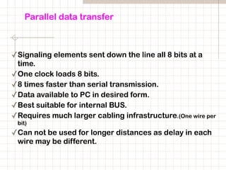
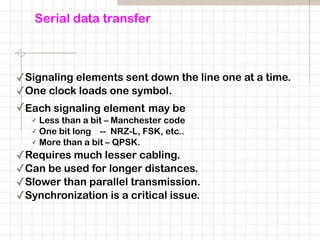
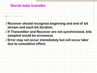
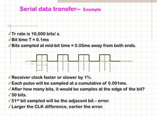
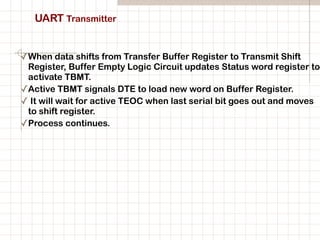
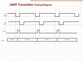
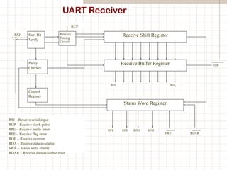
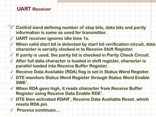
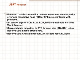

The document details various data transmission methods, focusing on parallel and serial transmission modes, as well as asynchronous and synchronous methods. It elaborates on the mechanics of UART and USRT for data conversion, error detection, and synchronization processes. Each method's advantages, disadvantages, and operational characteristics, including clock synchronization and bit transmission, are discussed in depth.