The document discusses the 8251 programmable communication interface chip. It provides 3 key points:
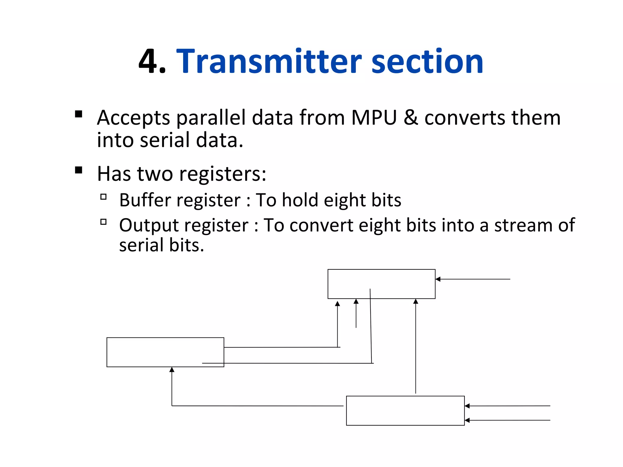
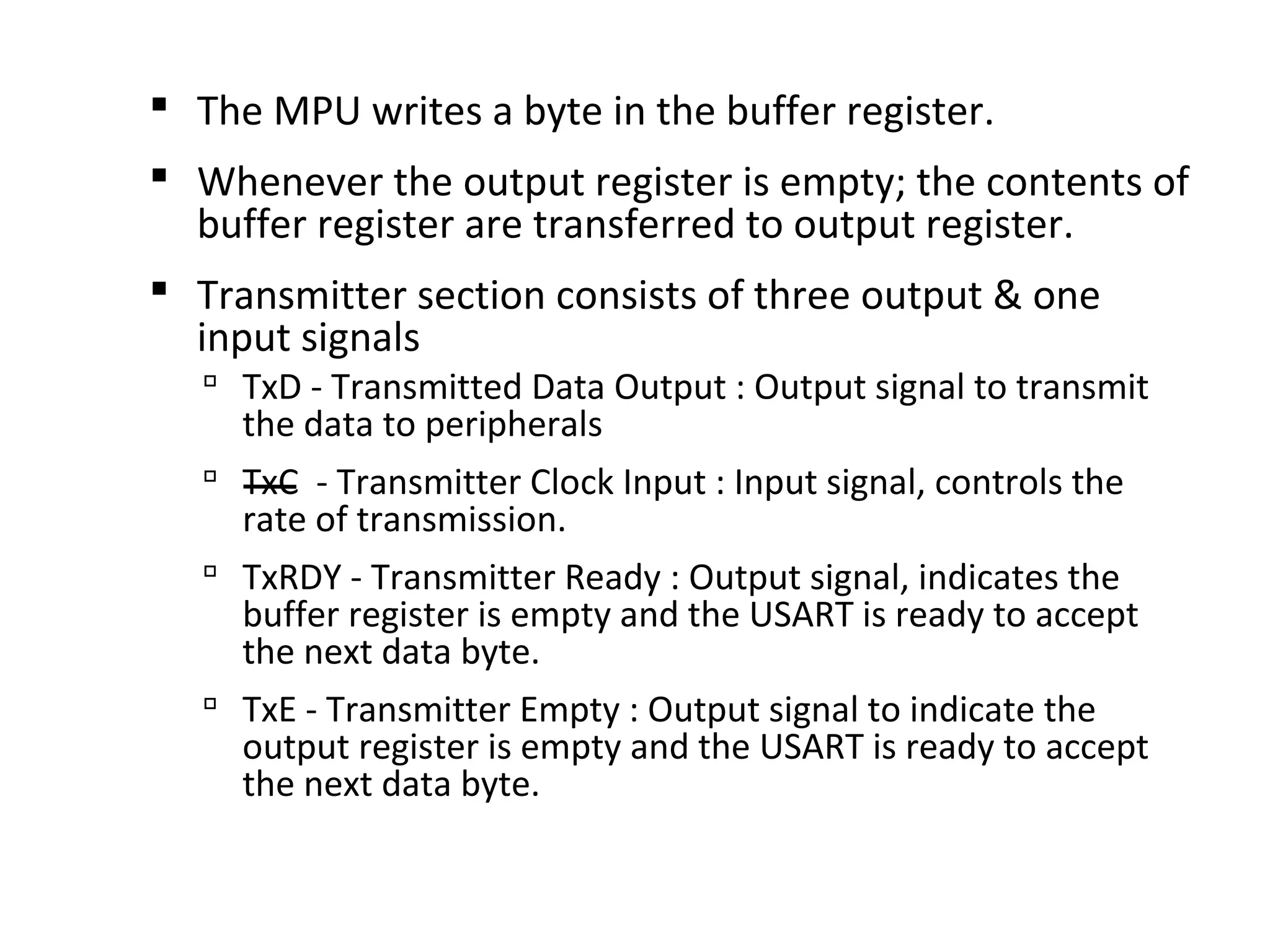
1. The 8251 is a USART (Universal Synchronous Asynchronous Receiver Transmitter) chip that allows for serial communication and converts parallel data from the CPU to serial data and vice versa.
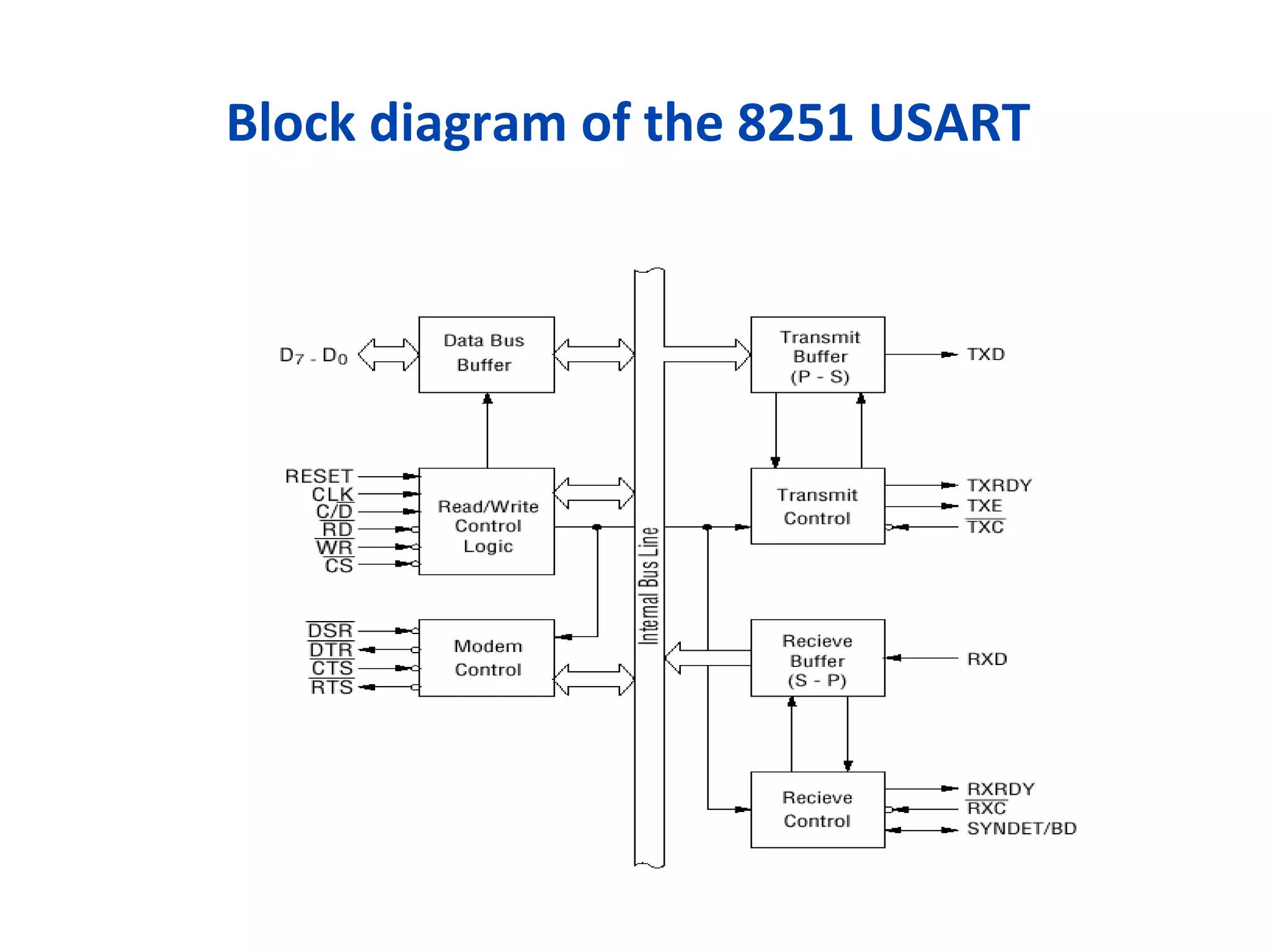
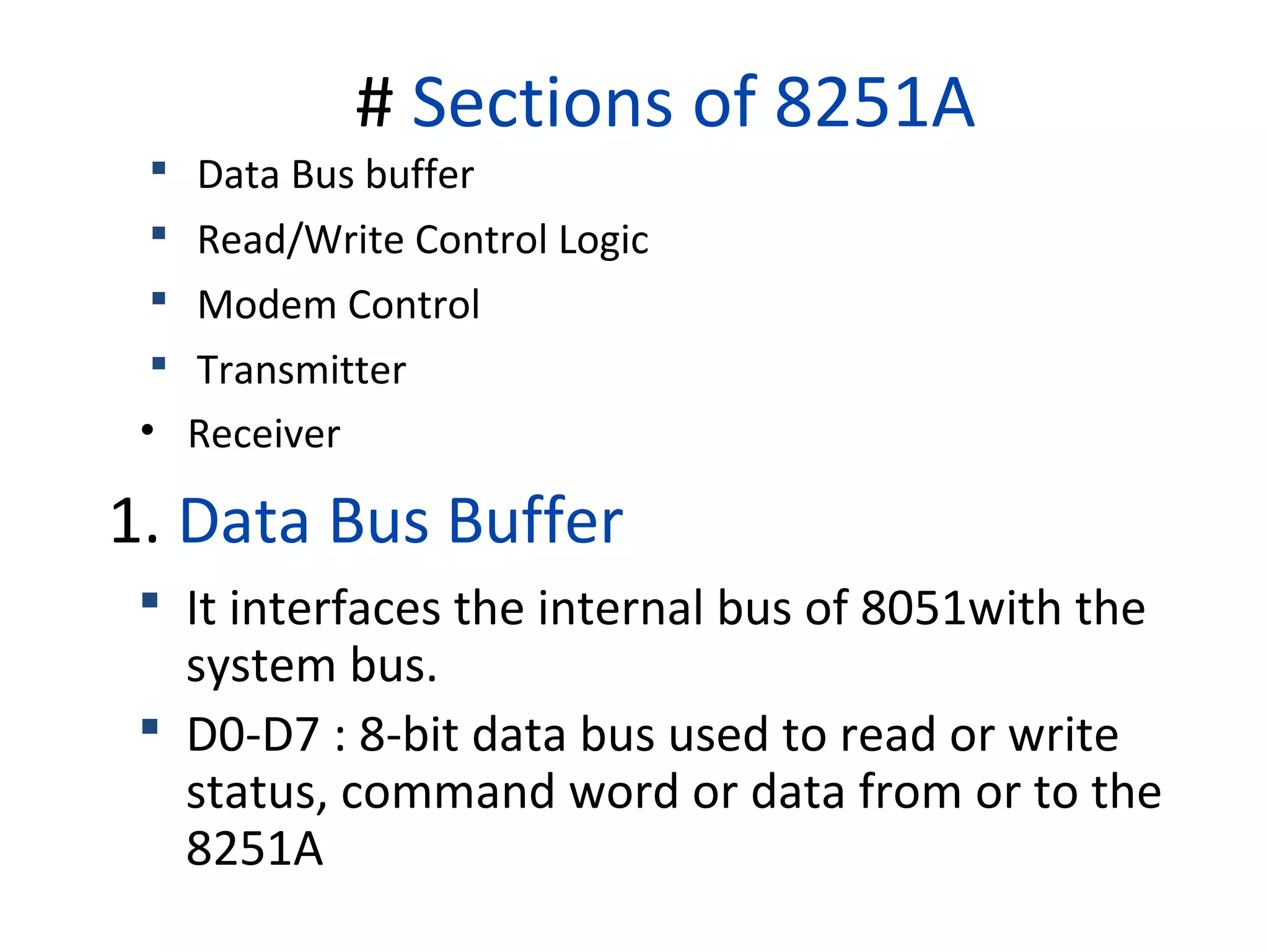
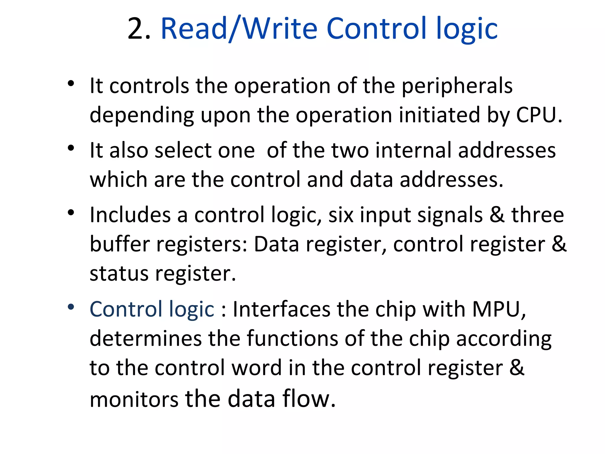
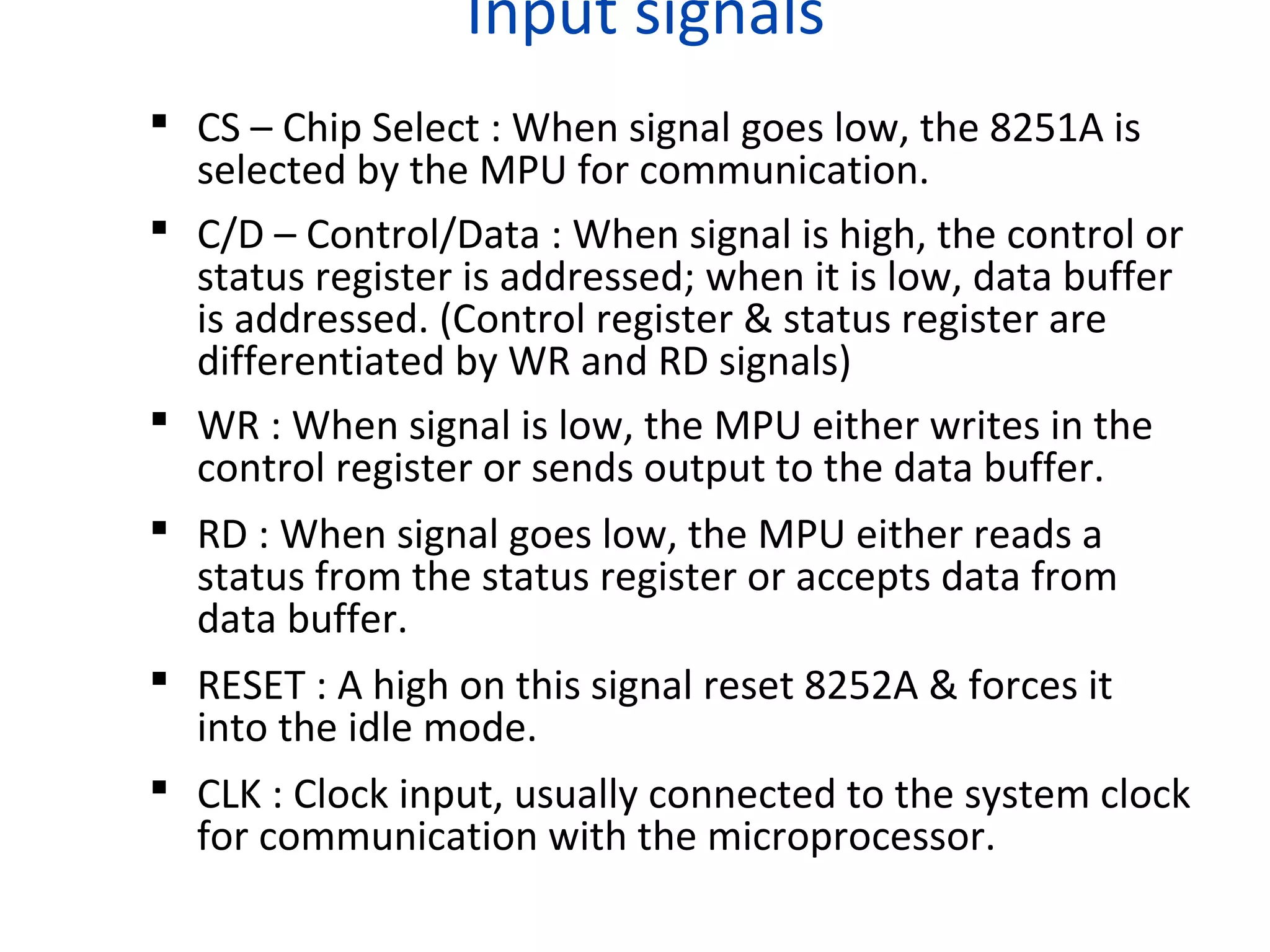
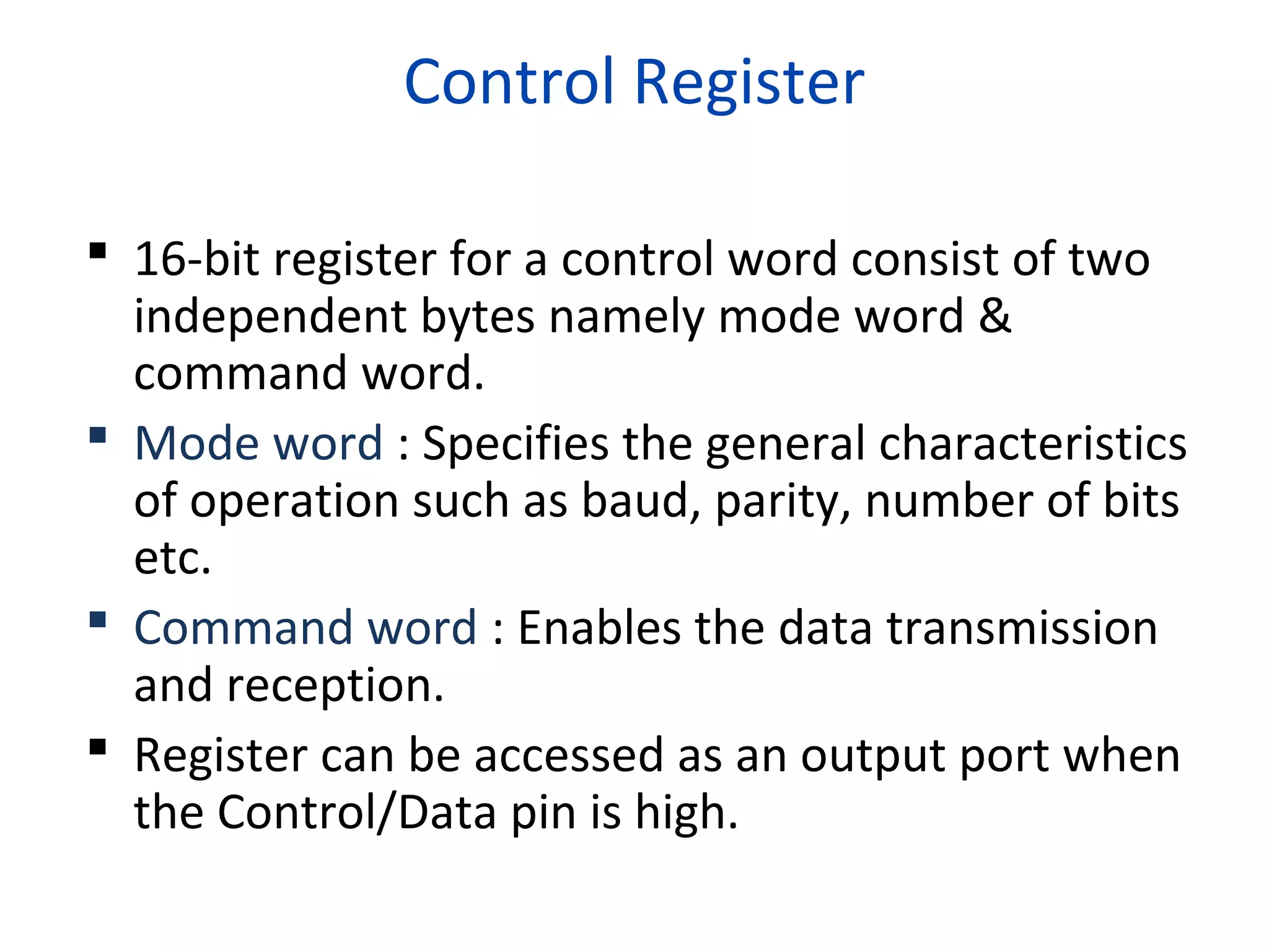
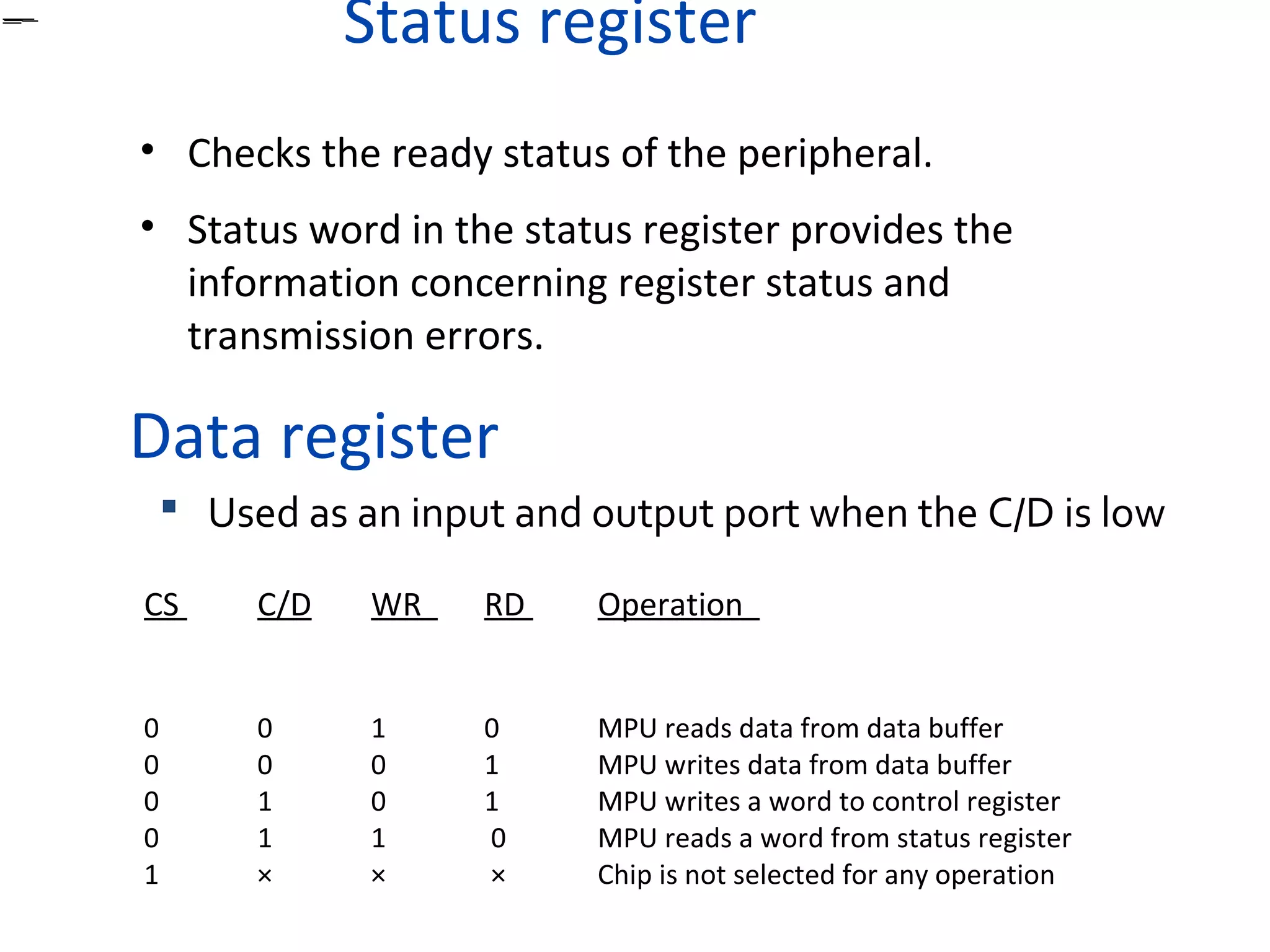
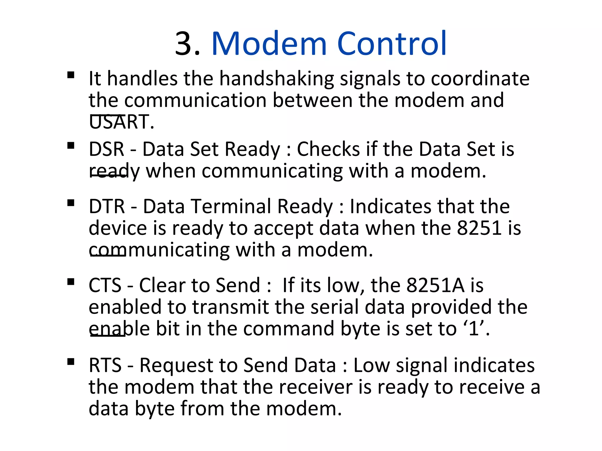
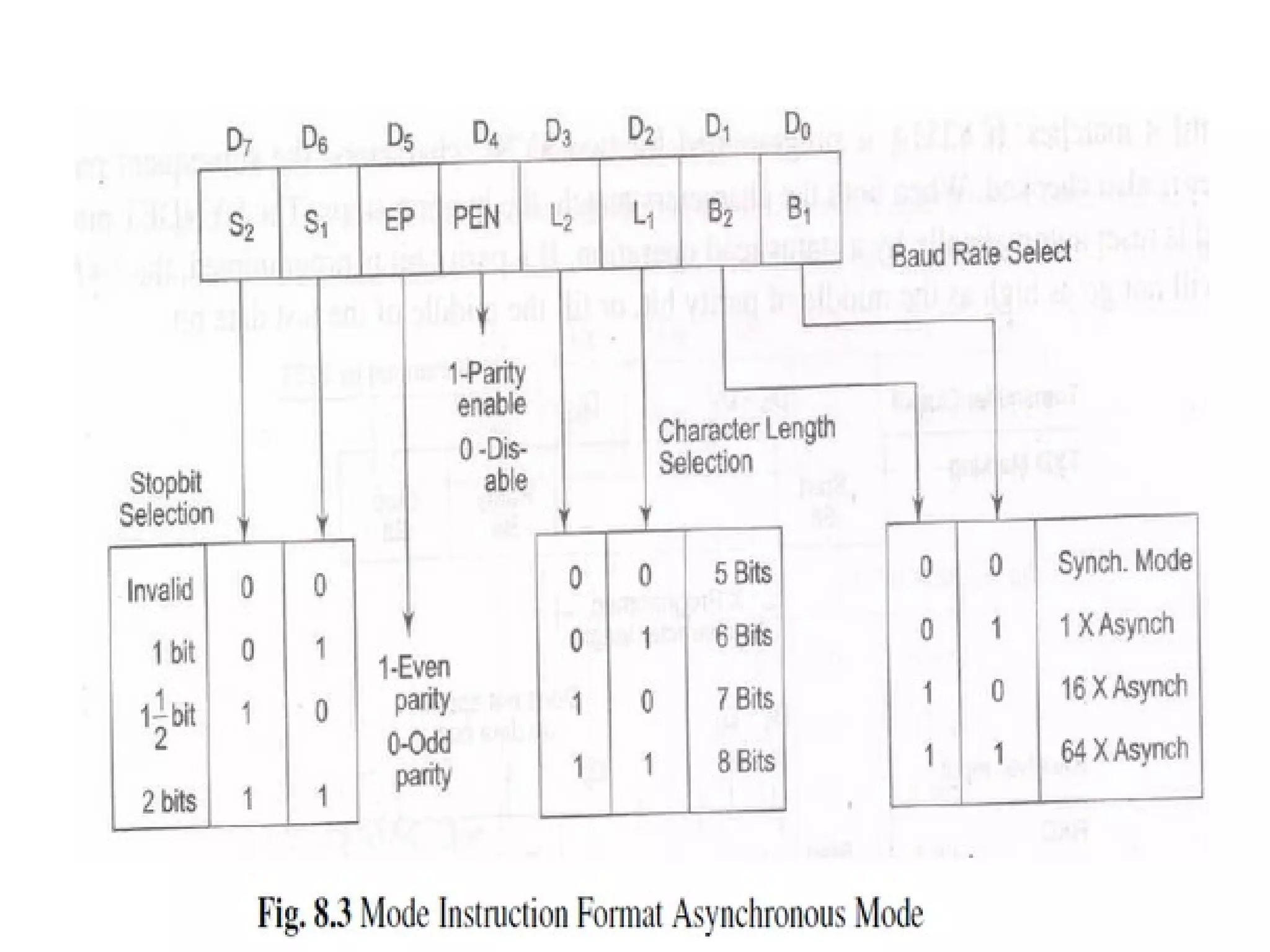
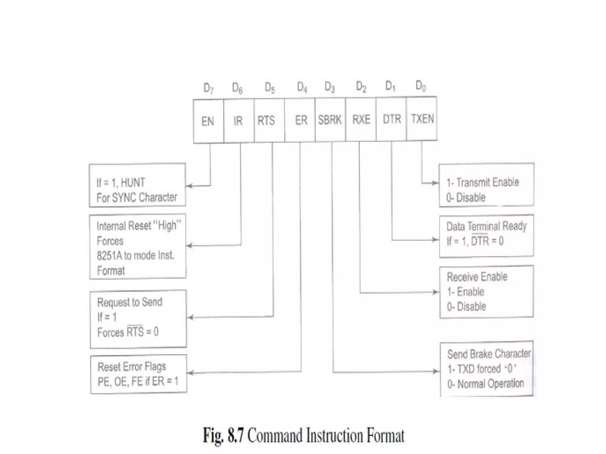
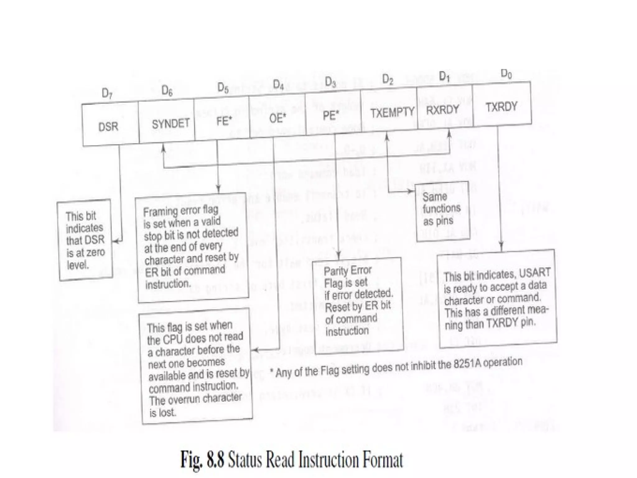
2. It has sections for data buffering, read/write control, modem control, transmission and reception. It uses control and status registers to program the chip for synchronous or asynchronous modes.
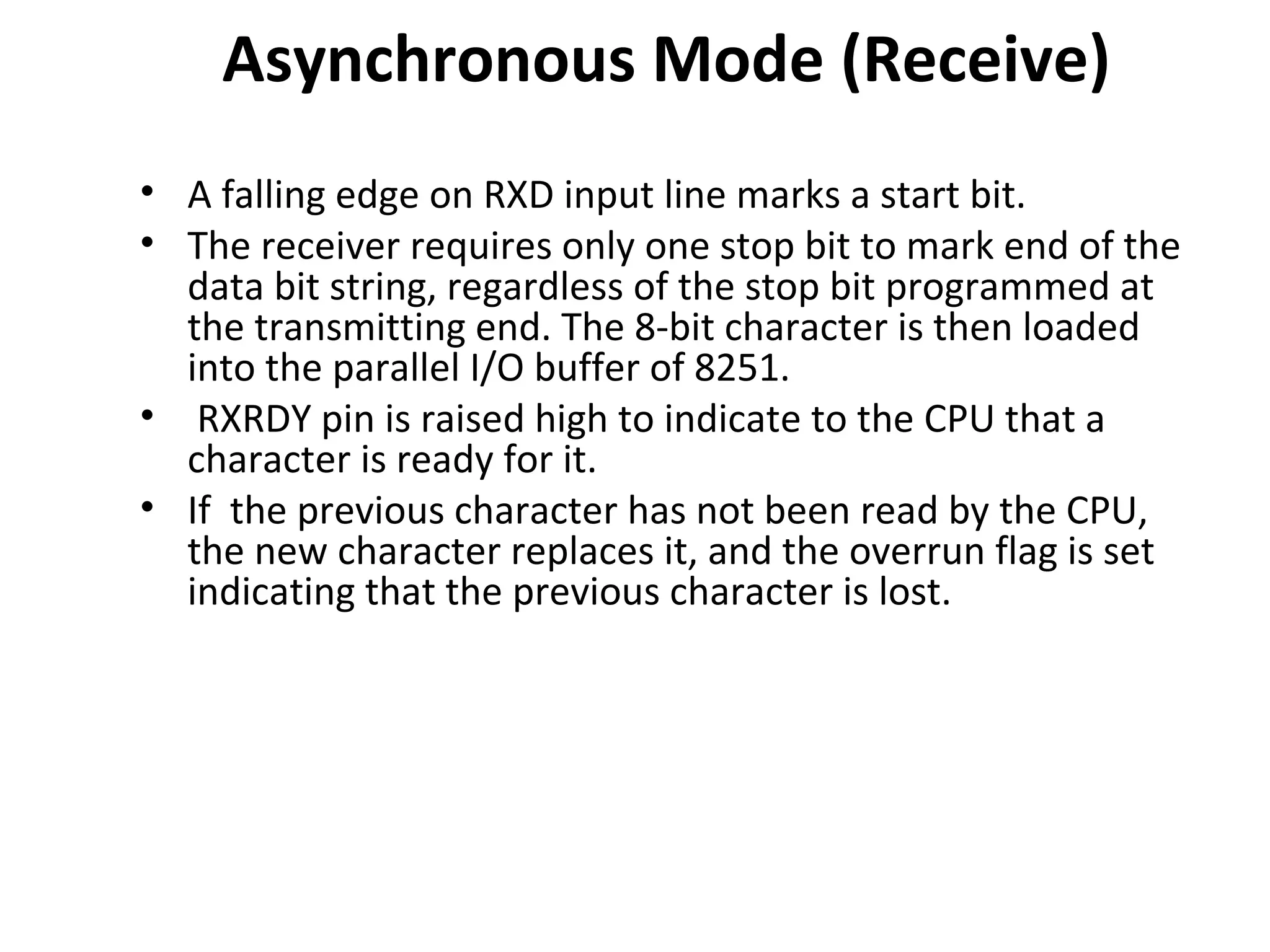
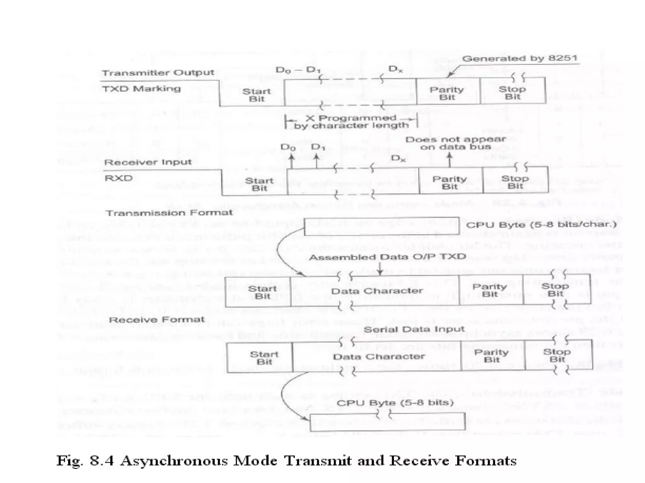
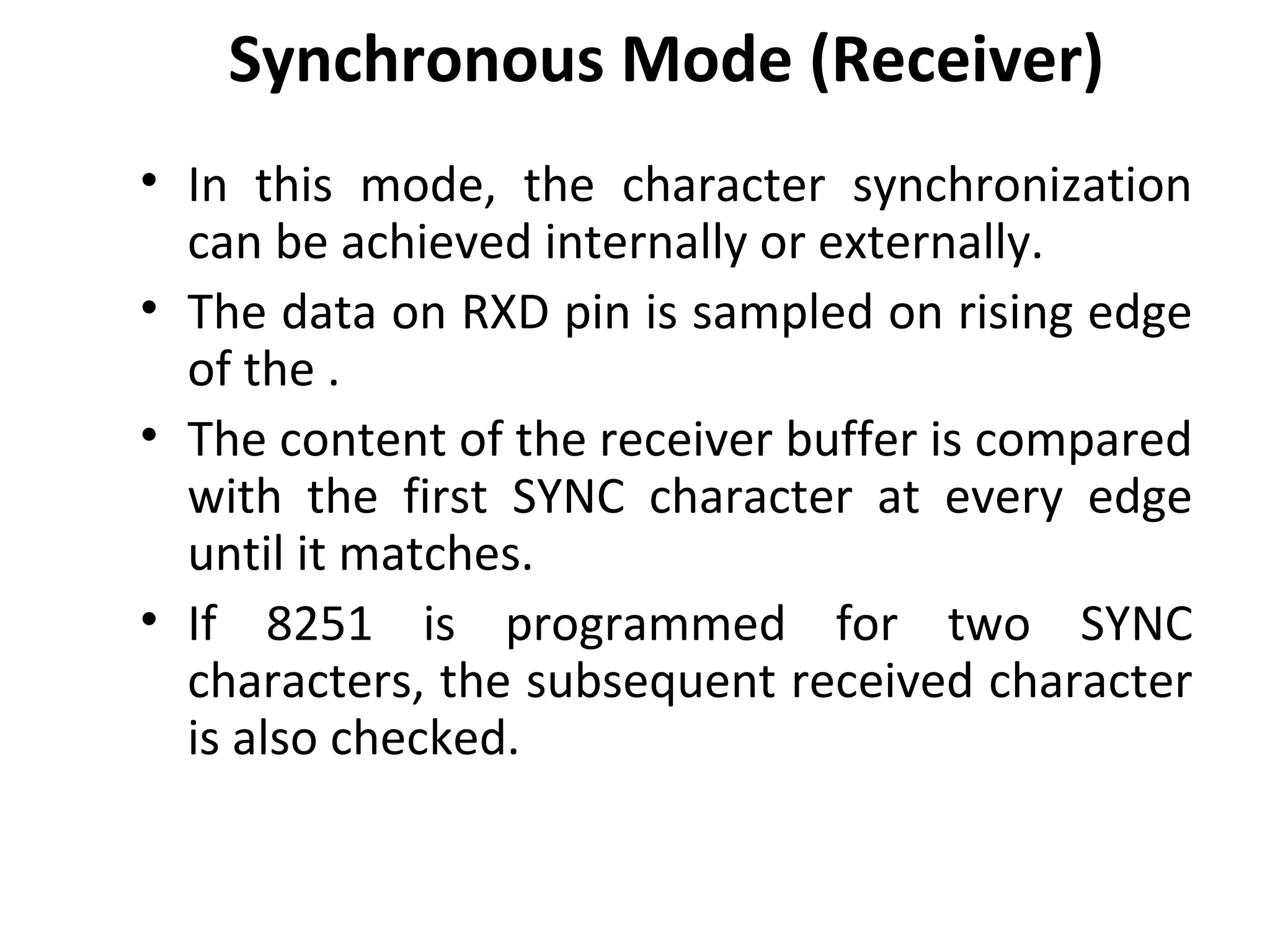
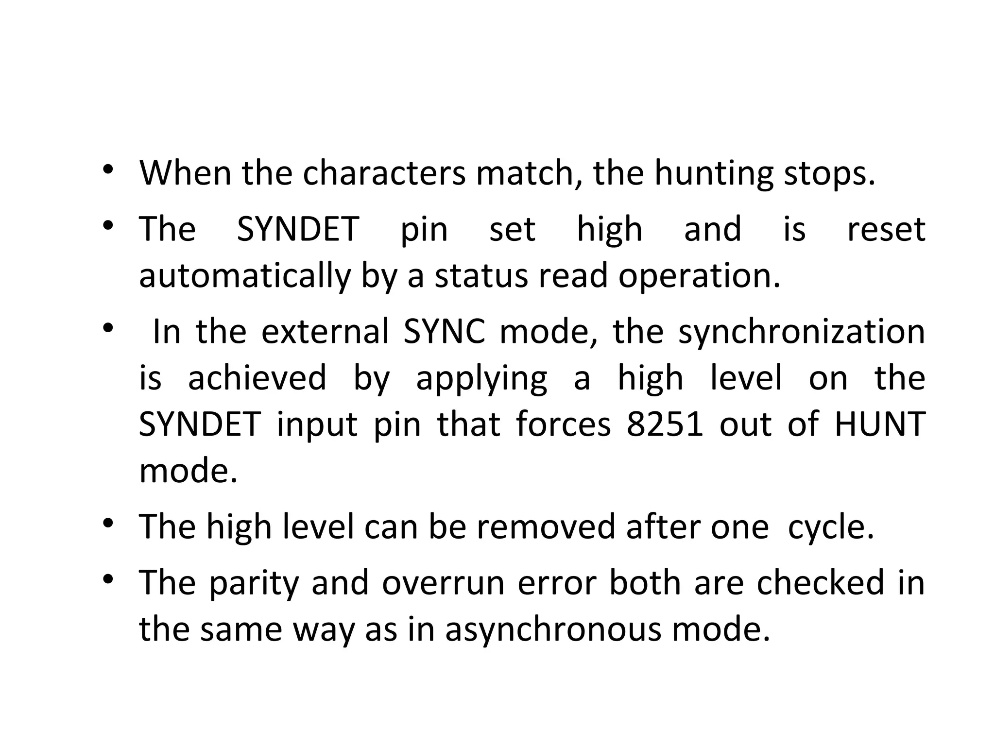
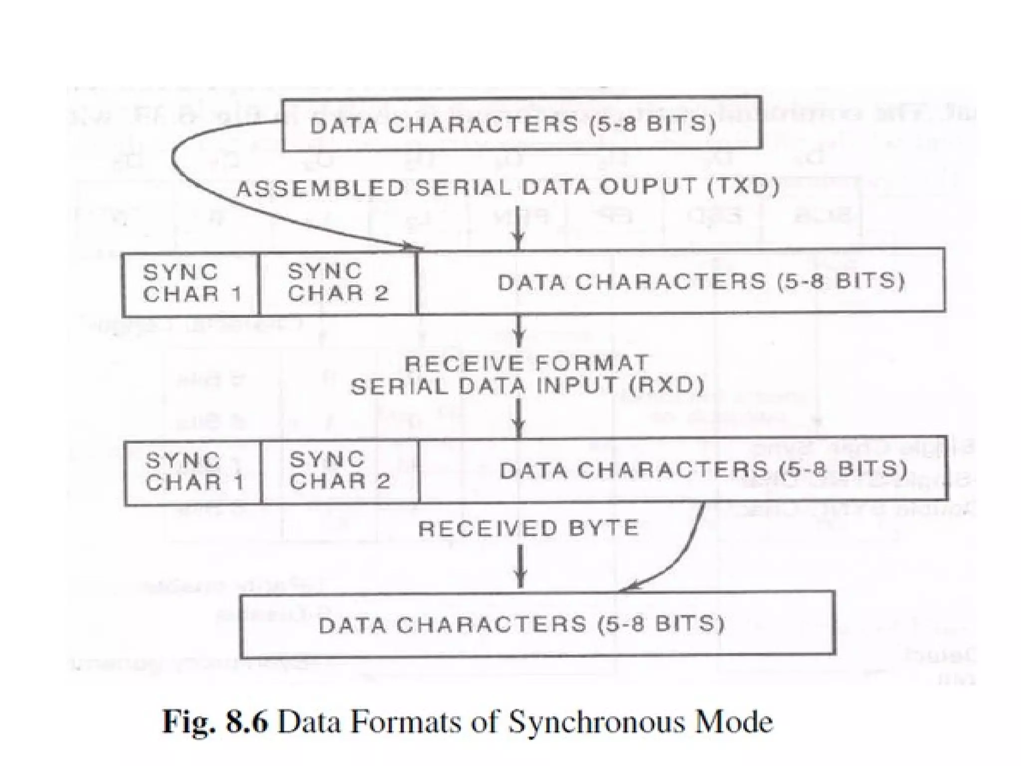
3. The chip can operate in asynchronous or synchronous modes. In asynchronous mode, it adds start and stop bits for transmission and looks for start/stop bits for reception. In synchronous mode, it uses sync characters