1) The document discusses the asynchronous and synchronous modes of the USART serial communication protocol for PIC microcontrollers.
2) In asynchronous mode, the USART can operate in either 8-bit or 9-bit mode and supports full-duplex communication. The baud rate is set using the SPBRG register.
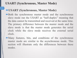
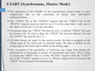
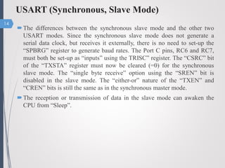
3) In synchronous master mode, the USART generates the serial clock and can only transmit or receive data at a time (half-duplex). The baud rate formula is different. In synchronous slave mode, the USART receives the external serial clock.