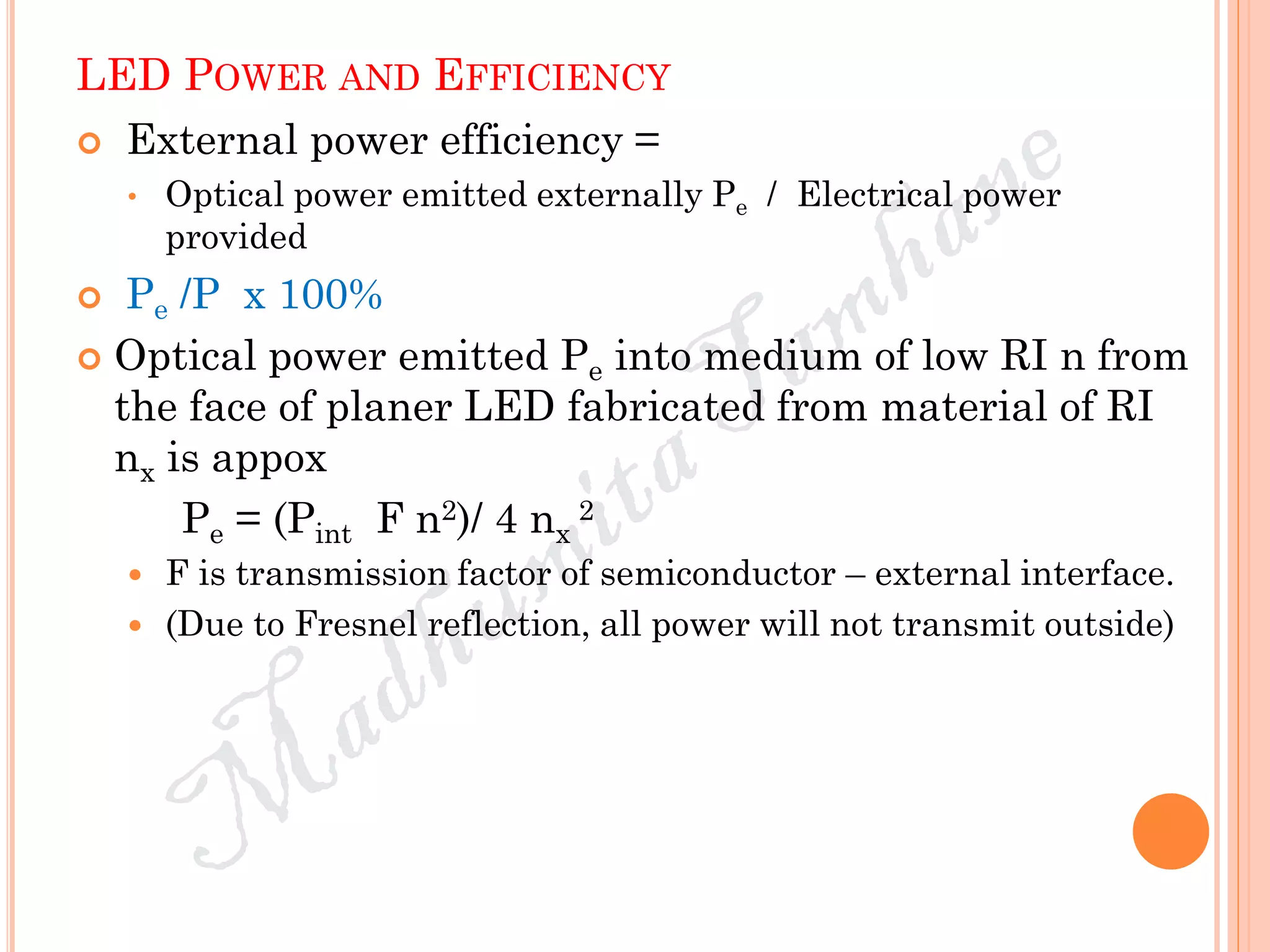
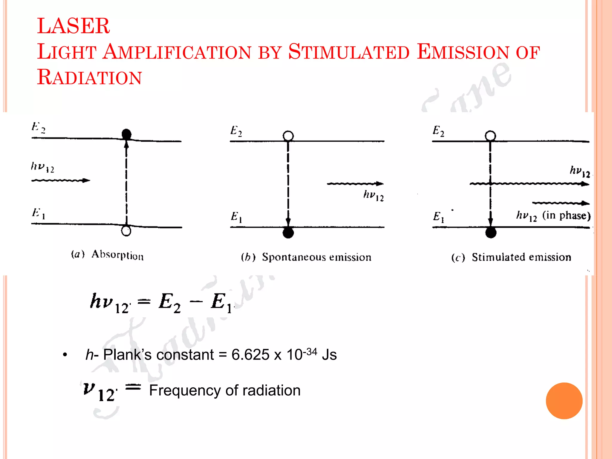
Downloaded 921 times


![LIMITATIONS OF MODULATION
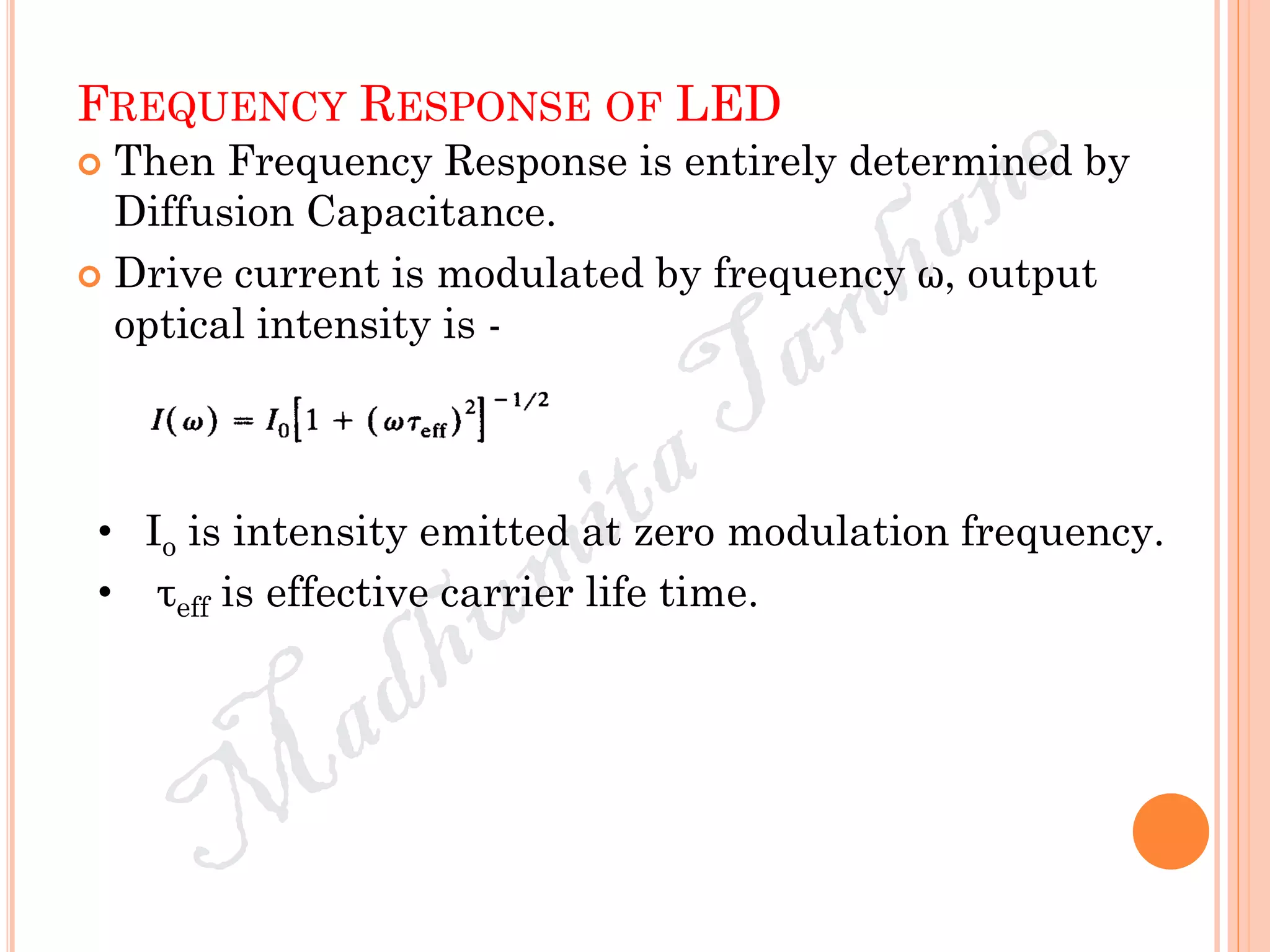
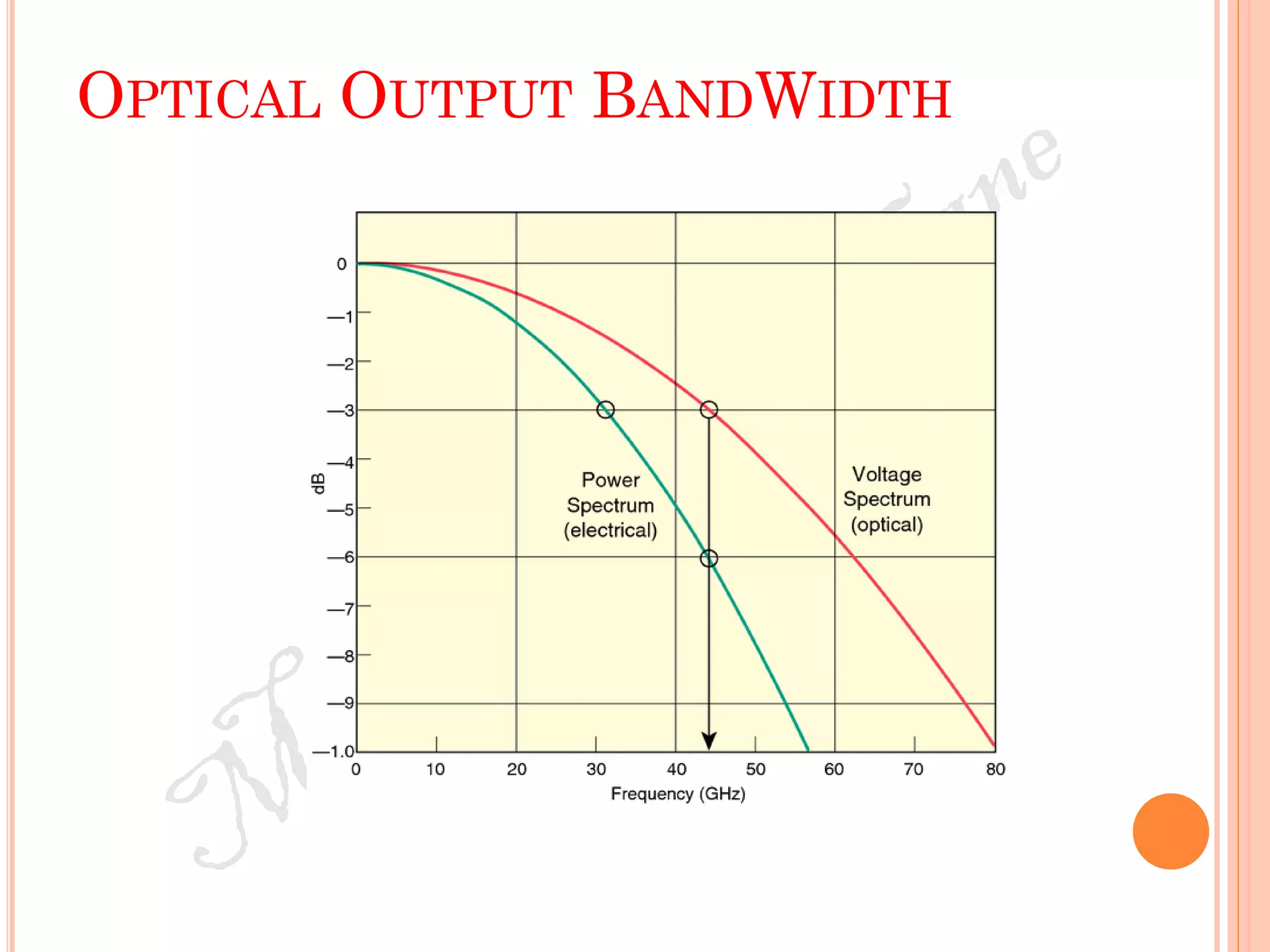
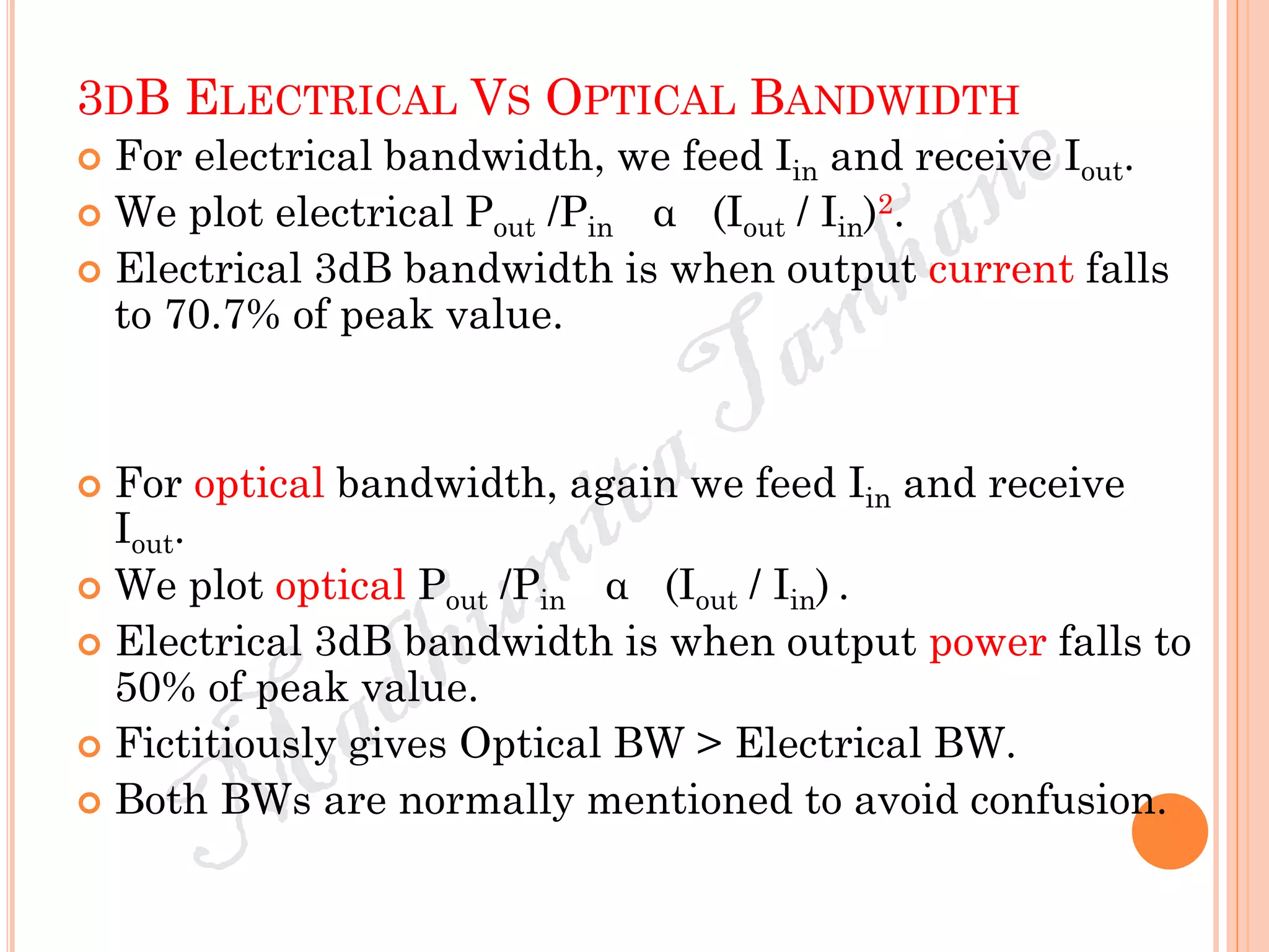
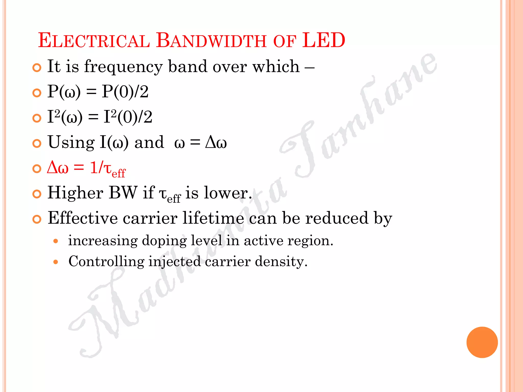
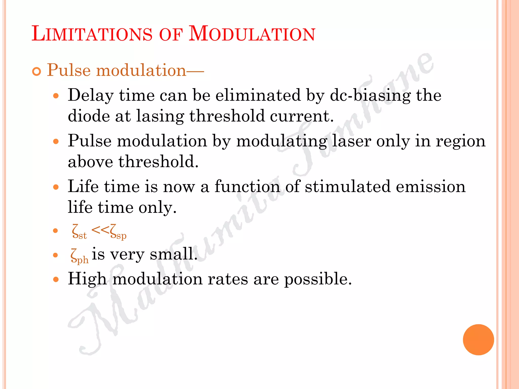
Pulse modulation—
Easy as photon life time is small.
During ‘0’ laser is off. ζsp limits the modulation rate.
Time required to achieved population inversion to
provide gain to overcome losses in cavity is td.
td = ζ ln [ Ip/(Ip + ( IB – Ith))]
Ip is current pulse amplitude.
IB is bias current.
ζ is average life time of carrier when Ip + IB = Ith](https://image.slidesharecdn.com/opticalfibercommunicationsourcesanddetectors-160426061235/75/Optical-fiber-communication-Part-2-Sources-and-Detectors-79-2048.jpg)


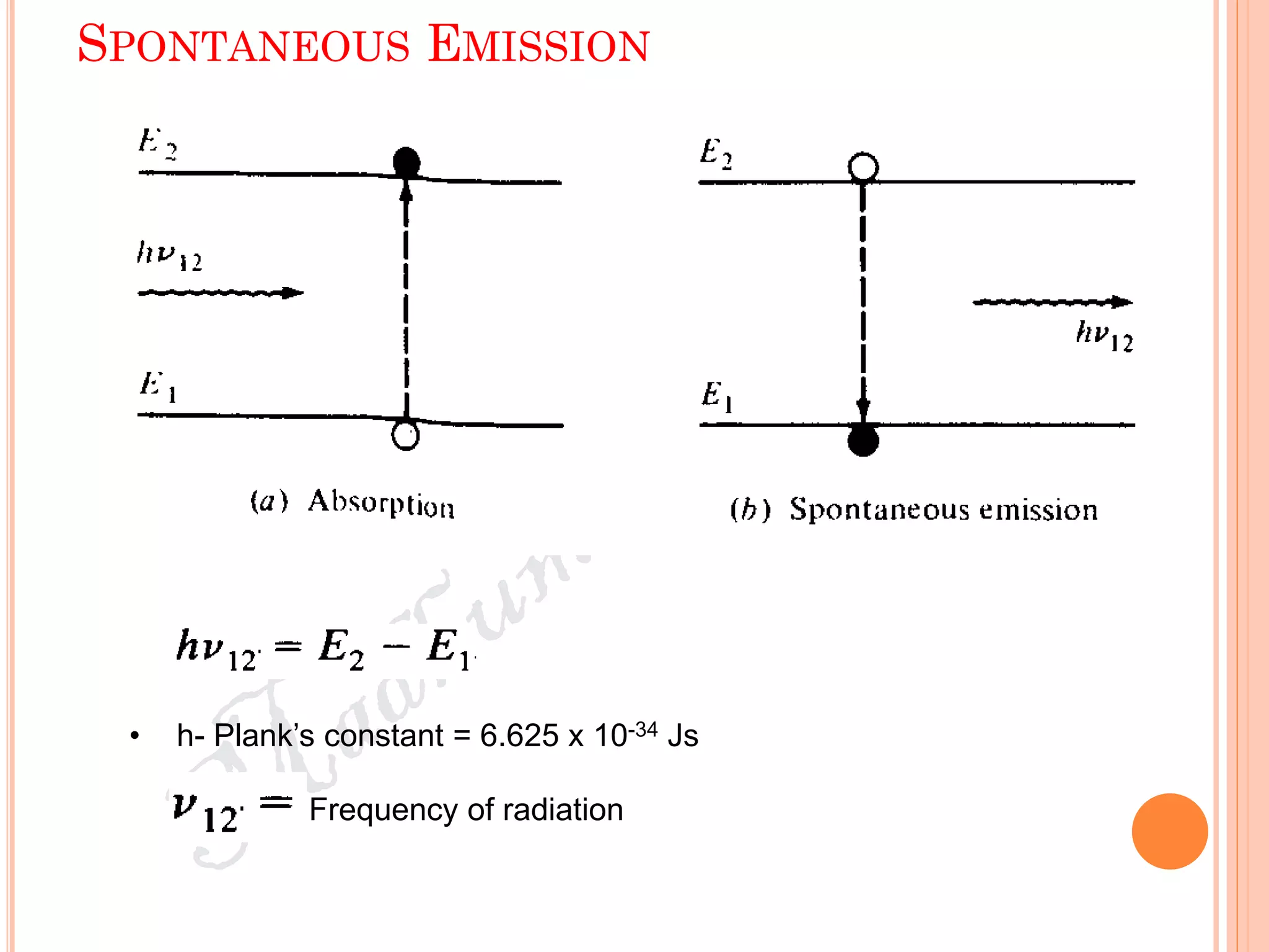
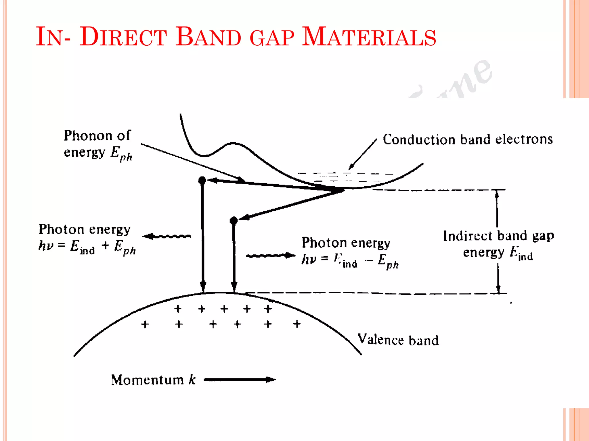
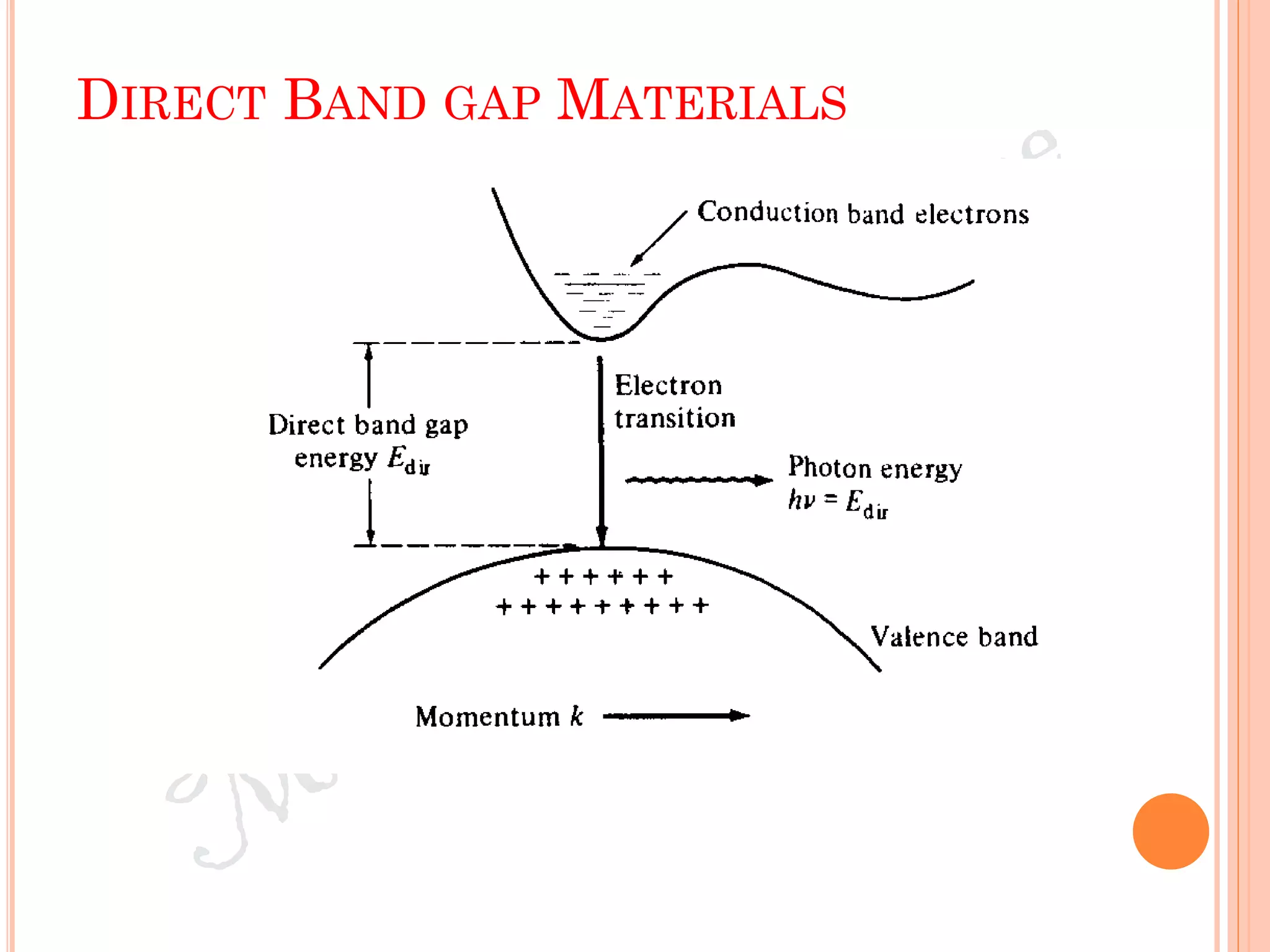
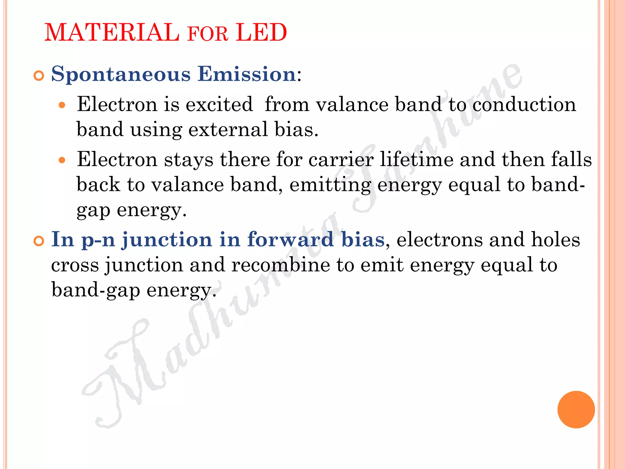
The document covers various aspects of optical fiber sources and detectors, focusing on materials, construction, efficiency, and the distinct characteristics of LEDs and lasers. It discusses the principles of spontaneous and stimulated emission, population inversion, and the mechanisms of light emission in different types of junctions. Additionally, it addresses modulation capabilities, response times, and factors influencing the performance of optical systems.