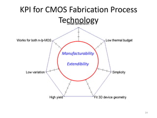
This document discusses challenges with continuing to scale CMOS fabrication processes beyond 22nm. It presents information on:
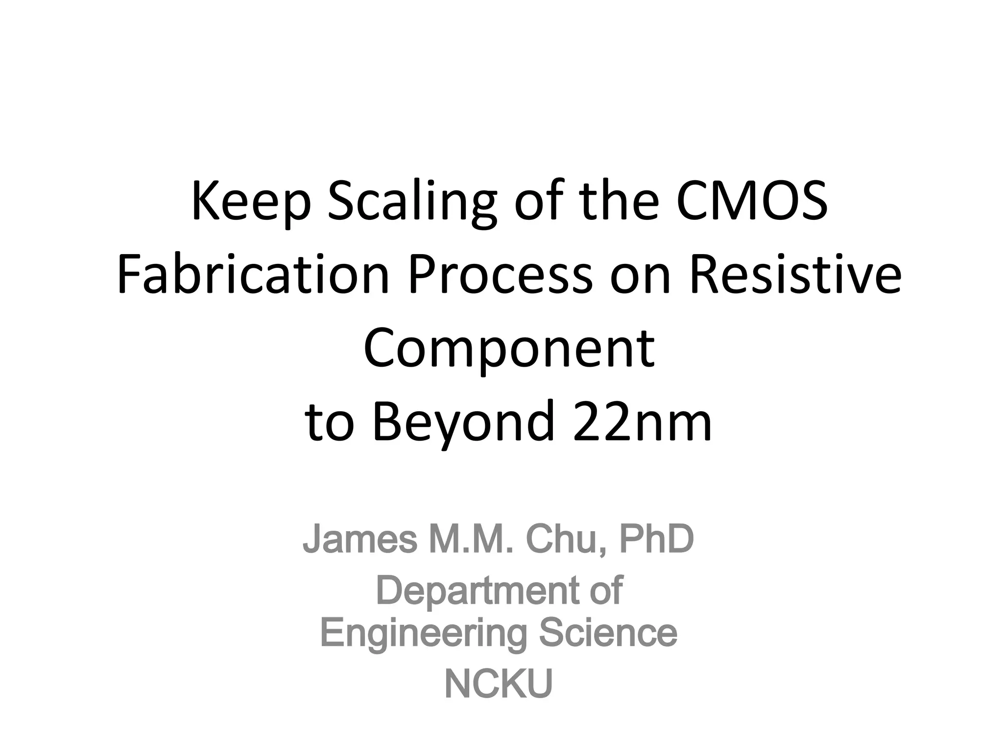
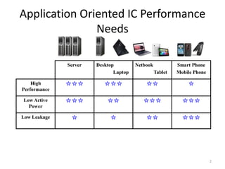
1) Application requirements for high performance, low power, and low leakage in different device types like servers, phones, etc.
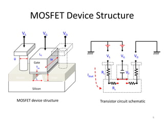
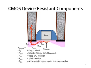
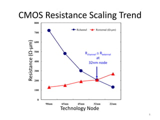
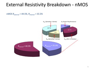
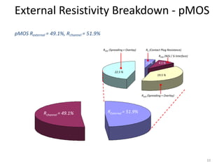
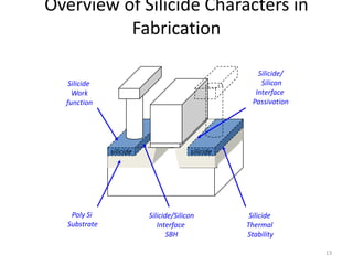
2) Trends in CMOS device resistance scaling and breakdown of external resistances like contact and silicide layers that contribute more at smaller nodes.
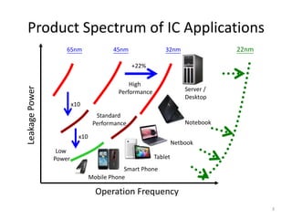
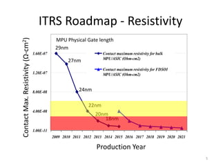
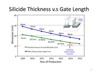
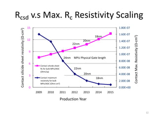
3) Projections that contact resistivity will exceed the ITRS roadmap target and require new materials to continue scaling beyond 22nm, along with thinner silicide layers required.