Downloaded 322 times

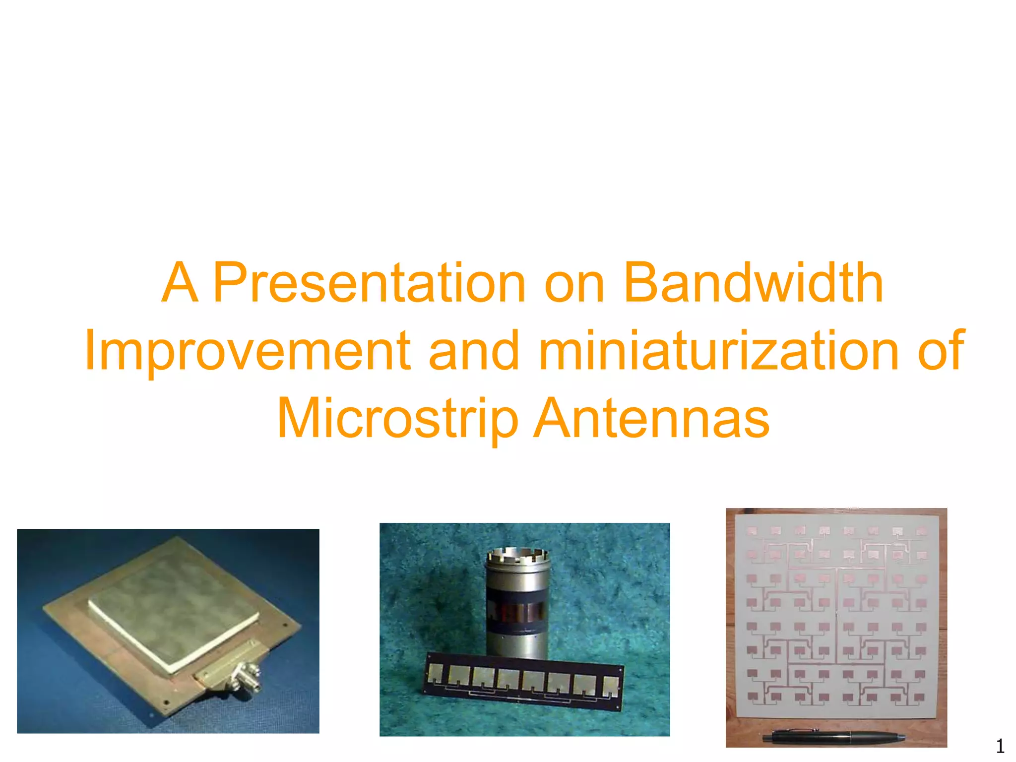
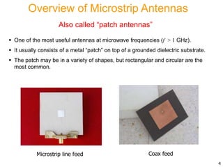
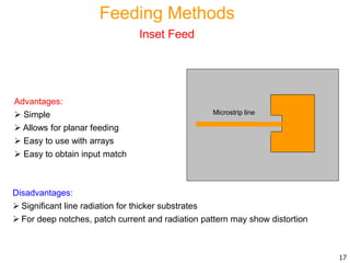
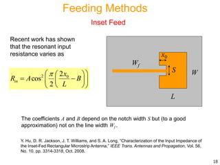
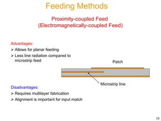
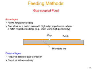


This document provides an overview of microstrip antennas and techniques for improving their bandwidth and miniaturization. It begins with an introduction to microstrip antennas, including their history, advantages, disadvantages, and applications. It then discusses various feeding methods, the basic cavity model principles of operation, and general characteristics such as bandwidth, resonance frequencies, and radiation efficiency. The document focuses on improving bandwidth through techniques such as changing the substrate thickness and permittivity or using special feeding methods. It also covers miniaturization methods such as modifying the patch shape or using stacked patches.


