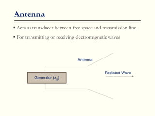
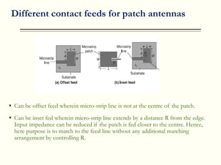
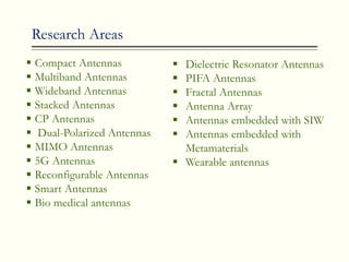
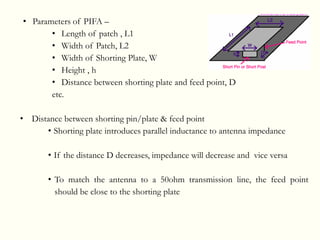
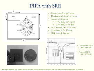
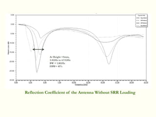
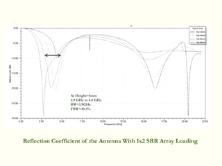
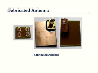
Basics of Antenna
Dr. Garima Saini
Assistant Professor
ECE Department
National Institute of Technical Teachers Training and Research
https://www.techtarget.com
Wireless Technology History & Future
Expectations
Antenna
 Acts as transducer between free space and transmission line
 For transmitting or receiving electromagnetic waves
Generator (zg)
Antenna
Radiated Wave
Antenna Categorization
Antenna
Categorization
Transmitting
Antenna
Receiving
Antenna
Transceiver
Antenna
Transmitting Antenna
 Designed to convert electrical signals into electromagnetic
waves and radiate them into space.
 The frequency of these waves is determined by the
frequency of the electrical signal applied to the antenna.
 Transmitting antennas are often optimized for specific
frequency ranges and directional characteristics, depending
on their intended applications..
Receiving Antenna
 Designed to capture incoming electromagnetic waves and
convert them into electrical signals that can be processed by a
receiving device.
 When electromagnetic waves from a distant source impinge
upon a receiving antenna, they induce a current in the
antenna's elements.
 This induced current carries the information contained in
the incoming waves, such as radio signals or data.
 Receiving antennas are also designed for certain frequency
bands.
Transreceiver
 Short for transmitter-receiver
 A device that combines both transmitting and receiving
functions in one unit.
 The transceiver switches between transmitting and receiving
modes as needed, allowing users to send and receive
information over the same antenna
Electromagnetic Spectrum
www.vodafone.co.uk
 The EM spectrum is typically divided into different fields:
radio waves, microwaves, infrared radiation, visible light,
ultraviolet, etc.
 The field order is determined by wavelength and frequency.
 = c/f
Electromagnetic Spectrum
www.vodafone.co.uk
Challenges in Antenna Design
Device
Antenna
Design
Challenges
Size
Small Size
Performance
Gain, Bandwidth etc.
Specific
Absorption
Rate
With globalisation or more spectrums bands released, antennas
will have to cover the new and existing spectrum bands.
Design
Solution Type
Creating Geometry
Geometry/Material
Analysis
Solution Setup
Frequency Sweep
Results
2D Reports
Field
Initial Project
Setup
Model
Setup
Solution
Setup
Viewing
Results
Boundaries
Excitation
Analyze
Simulation Using HFSS
Fabrication
Measurement
Antenna Design Flow
Microstrip Antenna
 A microstrip patch antenna consists of a conducting patch
of any geometry on one of the side of a dielectric substrate
with a ground plane on the other side.
 Choose the frequency –f0
 Choose the substrate
material
 Relative Permittivity of the
substrate - r
 Height of substrate- h
 Selection of Suitable geometry
 Suitable dielectric Substrate of appropriate thickness (h)
 Dielectric constant (εr ) and loss tangent (δ)
Parameter Selection
Thick substrate:
 Mechanically strong
 More radiated field
 Reduces conductor loss
 Improves impedance
bandwidth
Parameter Selection
Disadvantage:
 Increases the weight
 Increases Dielectric loss
 Increases Surface wave loss
 Dielectric constant (εr):
 If εr is high:
 Bandwidth becomes narrow because of
the loading effect
 Reduces the patch size, reduces the
radiation, increases the beamwidth.
Parameter Selection
Loss tangent (δ):
 A high loss tangent increases dielectric loss and therefore reduces the
antenna efficiency
Step 1: Calculation of the Width of patch
Step 2: Calculation of the Effective Dielectric Constant. This is based on the height,
dielectric constant of the dielectric and the calculated width of the patch antenna.
Step 3: Calculation of the Effective length
= c/f0, Wavelength
(i)
(ii)
(iii)
Step 4: Calculation of the length extension ΔL
Step5 : Calculation of actual length of the patch
f0 is the Resonance Frequency
W is the Width of the Patch
L is the Length of the Patch
h is the thickness
εr is the relative Permittivity of the dielectric substrate
c is the Speed of light: 3 x 10⁸
(iv)
(v)
Step 6: Calculation of the substrate length and width
Lg=L+ 6h
Wg= W+6h
h=0.0606/(r)
(vi)
Example:-
Frequency - 5GHz
C=3x10⁸m/s
εr =4.3
h=1.6mm
W=18.40mm
eff = 3.80
Leff = 15.39mm
l= 07298mm
L=13.93 mm, Lg = 23.55mm, Wg = 28mm
Feed design and its importance
 Feed design is an integral part of the design of actual antenna
 Success of feed design enables success in antenna design
 Many times, electronic systems are found not working properly for
wrong design of feed
 Sometimes special requirements might exist needing innovative feed
design to meet the user requirements
 Innovation in feed design is a continuous process and hence basic study
and understanding of feed design is very important.
Four common feeding methods of micro-strip patch antennas
 Micro-strip patch antenna can be
fed in variety of ways.
 Can be classified under contacting
and non-contacting feeds.
 In contacting method, RF power is
directly fed to the radiating patch
using a micro-strip line or coaxial
line.
 In non-contacting method,
electromagnetic coupling is done
through aperture coupling or
proximity coupling.
Coaxial or probe fed patch antenna
 Coaxial feed is a common feeding technique.
 Inner conductor extends through the dielectric and is soldered at the
top on the radiating patch.
 Advantage, feed can be placed at any desired location.
 Major disadvantage: Centre conductor protrudes in the dielectric,
Introduces inductance into the feed line leading to matching problems.
Also the probe may result in radiation in undesirable directions.
Centre
conductor
Different contact feeds for patch antennas
 Can be offset feed wherein micro-strip line is not at the centre of the patch.
 Can be inset fed wherein micro-strip line extends by a distance R from the edge.
Input impedance can be reduced if the patch is fed closer to the centre. Hence,
here purpose is to match to the feed line without any additional matching
arrangement by controlling R.
Different contact feeds for patch antennas
 Quarter wave line feed: Micro-strip antenna can be matched to a transmission line
of characteristic impedance Zo by using a quarter-wave section of characteristic
impedance Z1.
Zin=Zo=Z1 * Z1/ZA, where ZA is the antenna impedance.
Input impedance can be altered by suitable selection of Z1 so that Zin=Zo and the
antenna impedance is perfectly matched.
Non contacting feeds
 Aperture coupled, also called electromagnetic coupling scheme Fig a.
 Two dielectric substrate are used such that the feed line is sandwiched between the
two and radiating patch is on the top.
 Feed circuitry is shielded from the antenna by a conducting plane with a
hole/slot/aperture to transmit energy to the antenna.
 Coupling aperture is usually centered under the patch. Results in high bandwidth
about 13-20%.
Non contacting feeds
 Proximity coupled feed: Here the inset feed is stopped just before the patch antenna
feed point. Advantage is extra degree of freedom in design.
 Gap introduces a capacitance into the feed that can cancel out the inductance added
by the probe feed.
Comparison of feeding methods
Comparison of different feed methods
Different types of connectors in cable assemblies and N-type
connector with centre conductor protruded
SMA Connectors 2/4 hole flanges, PCB mountable, coaxial cable connectors
and adapters. For microstrip antenna feeding, flat centre conductor instead of
round one is suitable
Characteristic impedance of cables and
connectors
Research Areas
 Compact Antennas
 Multiband Antennas
 Wideband Antennas
 Stacked Antennas
 CP Antennas
 Dual-Polarized Antennas
 MIMO Antennas
 5G Antennas
 Reconfigurable Antennas
 Smart Antennas
 Bio medical antennas
 Dielectric Resonator Antennas
 PIFA Antennas
 Fractal Antennas
 Antenna Array
 Antennas embedded with SIW
 Antennas embedded with
Metamaterials
 Wearable antennas
Basic Antenna Research Objectives
 Enhancement of Bandwidth of MPA
 Gain Enhancement
 Size reduction of MPA
 Circular Polarization
 Multiband Performance
 Ultra-Wide Band Performance
 MIMO Antenna
 Mutual Coupling Reduction
Limitation of Existing Antenna
• Constraints on the personal communication antenna is
• Size miniaturization
• Good bandwidth
• Gain
• Microstrip patch antenna has narrow bandwidth
• Very limited scope of further miniaturization
• PIFA antenna is one of the promising candidate for personal communication
Why Planar Inverted F Antenna?
• PIFA antenna is
• Easy to hide in the casing of the mobile
handset as compared to monopole, rod & helix
antennas
• Reduced backward radiation towards user’s
head and body which further minimizes SAR
and improves performance
• They can resonate at much smaller antenna size
• By cutting slots in radiating patch, resonance
can be modified
• Parameters of PIFA –
• Length of patch , L1
• Width of Patch, L2
• Width of Shorting Plate, W
• Height , h
• Distance between shorting plate and feed point, D
etc.
• Distance between shorting pin/plate & feed point
• Shorting plate introduces parallel inductance to antenna impedance
• If the distance D decreases, impedance will decrease and vice versa
• To match the antenna to a 50ohm transmission line, the feed point
should be close to the shorting plate
• Design equations (in general)
• L1+L2-w=( /4 )+ h
• If w =0 , L1+ L2= ( /4) + h
• Fr = c/4(L1+L2-h)
• The major drawback of PIFA is its narrow bandwidth thus need
• to widen the bandwidth for using it in mobile phones and other handheld
devices.
• Some of the techniques to Improve the bandwidth
• Increase the height of shorting plate
• Reducing the ground plane
• Slot / split ring loading
• Capacitive Loading
• Change in Feed plate Width
• Meandering shorting strip
• superstrate etc.
Slit in ground plane edge can lower the Q factor of
structure and results in increase in BW
• Metamaterial can have their electromagnetic properties altered to something
beyond what can be found in nature.
• These structures can be realised artificially by creating the composite
structures of two concentric Split ring printed on substrate.
• SRR can be in any shapes like square, rectangular, ring, triangular and ohm
shaped structure etc.
• Shape & size of SRRs can be different as per design requirement and its
application domain.
Metamaterial
PIFA with SRR
Neha Yadav* and Garima Saini, Split Ring Resonator Based Wide Bandwidth Planar Inverted-F Antenna for Wi-Fi/WLAN Applications, I J C T A, 9(18) 2016, pp. 9027-9034
• Size of the slot, g=2 mm
• Thickness of rings, c=1 mm
• Radius of rings are
• r1=2 mm, r2=3 mm
• r3=4 mm, r4=5 mm
• Ls =20 mm , Ws = 20 mm,
• L1= 8mm, L2= 12mm
• FR4, r=4.4, 16mm
• Conventional PIFA
• BW-1.68 GHz
• Proposed PIFA
• BW= 1.95GHz
Design of metamaterial based PIFA of reduced size and volume
with high gain
Top view; Side view; PIFA loaded with 1x2 SRR Array and 2x2 SRR array configurations on the
inner side of the radiating top plate
• For UWB Application
Parameter
Dimension
(mm)
do 0.5
di 0.5
c 0.5
r2 2
r0 1.5
r1 1
rin 0.5
Ws 3
Wf 4
SRR Dimensions
• Ground plane: 37.6mm x 26.4mm
• Radiating top plate: 10mmx16mm
• Shorting plate width: 3mm
• Height of the top plate: Varied from
3mm to 6mm
Circular SRR
Reflection Coefficient of the Antenna Without SRR Loading
At Height =5mm,
3.1GHz to 4.9 GHz
BW = 1.8GHz
FBW= 45%
Reflection Coefficient of the Antenna With 1x2 SRR Array Loading
At Height=5mm
2.9 GHz to 4.8 GHz
BW=1.9GHz
FBW=49.3%
Reflection Coefficient of the antenna with 2x2 SRR Loading
At Height=5mm
2.9 GHz to 4.9 GHz
BW=2GHz
FBW=68.9%
3D Polar Plot at 3.6GHz of PIFA antenna (a) Without SRR, (b) With 1x2 SRR Array
Loading; and 3D Polar Plot at 3.4GHz with 2x2 SRR Array Loading
(a) (b)
(c)
Attia, H., Bait-Suwailam, M. M., and Ramahi, O. M., (2010), “Enhanced Gain Planar Inverted-F Antenna with Metamaterial Superstrate for
UMTS Applications,” Progress In Electromagnetics Research Online, 6(6), pp. 585-588.
• Magnetic superstrate constituted by SRR printed on both sides of a dielectric
slab is designed for gain enhancement
• Dimensions of 24mm X 8mm
• 12X12 array of SRRs, consists of 3 layers , Layers are separated by 2 mm
of air layers , 8.5mm ht. of shorting plate from ground
• Improvement of 3.2dB gain is observed
PIFA with Superstrate
SRR Array Embedded PIFA
• For the enhancement of antenna gain , researchers reported use of superstrate
layer above MPA
• Study of different configurations of SRR array on the inner side of radiating
plate of PIFA for gain enhancement
Top & Side View PIFA
• PIFA Dimensions
• L1 x W1- 30mm x 30 mm
• L2 x W2- 10mm x 16mm
• S x H- 5mm x 6mm
• Without SRR, Resonant frequency -
3.5GHz
• SRR unit cell dimensions
• c==w=0.5mm
• r1=2mm ,.r2=1mm
SRR unit cell
Different SRR configurations
Antenna design using different SRR configurations
Top view & Side view of the antenna
• For LTE-Hi Applications
Reflection Coefficient of PIFA with different configurations of
SRR
Resonating Frequency and Bandwidth for different SRR Configuration
Fabricated Antenna
Parameters
Resonating
Frequency
(GHz)
Bandwidth
(MHz)
Return Loss
(dB)
Gain
Without SRR 3.5 1320 -27.4 7.1
With
SRR
Arra
y
A 3.39 1290 -31.9 8.1
B 3.4, 14.6 1280, 230 -44.2, -16.6 7.18, 4.67
C 3.3 1230 -25.5 13.2
D 2.9, 3.4 1290 -24.8, -35.5 14.9, 11.5
E 3.2, 3.8, 14.5 1140, 250 -22, -26.6, -16.9 8.84, 17.1, 4.5
Simulated and Measured return loss of PIFA with Configuration
‘E’
• A good impedance matching is achieved in the frequency
range from 2.6 - 3.9 GHz
Simulated & Measured Results
Polar plot of PIFA with configuration ‘E’ at 3.2 GHz, 3.8 GHz, 14.5 GHz
Fabricated Antenna
Fabricated Antenna
Measured and simulated radiation pattern of PIFA of configuration-4
Experimental setup to observe the
radiation pattern of PIFA loaded
with SRR of configuration-4
References and Acknowledgements
 Antenna Engineering Handbook, 3rd Edition, Richard Johnson
 Antennas and wave propagation , fifth edition,
John D Kraus
 Internet open source-Images
Thank You

antennas ppt.pdf

  • 1.
    Basics of Antenna Dr.Garima Saini Assistant Professor ECE Department National Institute of Technical Teachers Training and Research
  • 2.
  • 3.
    Antenna  Acts astransducer between free space and transmission line  For transmitting or receiving electromagnetic waves Generator (zg) Antenna Radiated Wave
  • 4.
  • 5.
    Transmitting Antenna  Designedto convert electrical signals into electromagnetic waves and radiate them into space.  The frequency of these waves is determined by the frequency of the electrical signal applied to the antenna.  Transmitting antennas are often optimized for specific frequency ranges and directional characteristics, depending on their intended applications..
  • 6.
    Receiving Antenna  Designedto capture incoming electromagnetic waves and convert them into electrical signals that can be processed by a receiving device.  When electromagnetic waves from a distant source impinge upon a receiving antenna, they induce a current in the antenna's elements.  This induced current carries the information contained in the incoming waves, such as radio signals or data.  Receiving antennas are also designed for certain frequency bands.
  • 7.
    Transreceiver  Short fortransmitter-receiver  A device that combines both transmitting and receiving functions in one unit.  The transceiver switches between transmitting and receiving modes as needed, allowing users to send and receive information over the same antenna
  • 8.
    Electromagnetic Spectrum www.vodafone.co.uk  TheEM spectrum is typically divided into different fields: radio waves, microwaves, infrared radiation, visible light, ultraviolet, etc.  The field order is determined by wavelength and frequency.  = c/f
  • 9.
  • 10.
    Challenges in AntennaDesign Device Antenna Design Challenges Size Small Size Performance Gain, Bandwidth etc. Specific Absorption Rate With globalisation or more spectrums bands released, antennas will have to cover the new and existing spectrum bands.
  • 11.
    Design Solution Type Creating Geometry Geometry/Material Analysis SolutionSetup Frequency Sweep Results 2D Reports Field Initial Project Setup Model Setup Solution Setup Viewing Results Boundaries Excitation Analyze Simulation Using HFSS Fabrication Measurement Antenna Design Flow
  • 12.
    Microstrip Antenna  Amicrostrip patch antenna consists of a conducting patch of any geometry on one of the side of a dielectric substrate with a ground plane on the other side.  Choose the frequency –f0  Choose the substrate material  Relative Permittivity of the substrate - r  Height of substrate- h
  • 13.
     Selection ofSuitable geometry  Suitable dielectric Substrate of appropriate thickness (h)  Dielectric constant (εr ) and loss tangent (δ) Parameter Selection
  • 14.
    Thick substrate:  Mechanicallystrong  More radiated field  Reduces conductor loss  Improves impedance bandwidth Parameter Selection Disadvantage:  Increases the weight  Increases Dielectric loss  Increases Surface wave loss
  • 15.
     Dielectric constant(εr):  If εr is high:  Bandwidth becomes narrow because of the loading effect  Reduces the patch size, reduces the radiation, increases the beamwidth. Parameter Selection Loss tangent (δ):  A high loss tangent increases dielectric loss and therefore reduces the antenna efficiency
  • 16.
    Step 1: Calculationof the Width of patch Step 2: Calculation of the Effective Dielectric Constant. This is based on the height, dielectric constant of the dielectric and the calculated width of the patch antenna. Step 3: Calculation of the Effective length = c/f0, Wavelength (i) (ii) (iii)
  • 17.
    Step 4: Calculationof the length extension ΔL Step5 : Calculation of actual length of the patch f0 is the Resonance Frequency W is the Width of the Patch L is the Length of the Patch h is the thickness εr is the relative Permittivity of the dielectric substrate c is the Speed of light: 3 x 10⁸ (iv) (v)
  • 18.
    Step 6: Calculationof the substrate length and width Lg=L+ 6h Wg= W+6h h=0.0606/(r) (vi) Example:- Frequency - 5GHz C=3x10⁸m/s εr =4.3 h=1.6mm W=18.40mm eff = 3.80 Leff = 15.39mm l= 07298mm L=13.93 mm, Lg = 23.55mm, Wg = 28mm
  • 19.
    Feed design andits importance  Feed design is an integral part of the design of actual antenna  Success of feed design enables success in antenna design  Many times, electronic systems are found not working properly for wrong design of feed  Sometimes special requirements might exist needing innovative feed design to meet the user requirements  Innovation in feed design is a continuous process and hence basic study and understanding of feed design is very important.
  • 20.
    Four common feedingmethods of micro-strip patch antennas  Micro-strip patch antenna can be fed in variety of ways.  Can be classified under contacting and non-contacting feeds.  In contacting method, RF power is directly fed to the radiating patch using a micro-strip line or coaxial line.  In non-contacting method, electromagnetic coupling is done through aperture coupling or proximity coupling.
  • 21.
    Coaxial or probefed patch antenna  Coaxial feed is a common feeding technique.  Inner conductor extends through the dielectric and is soldered at the top on the radiating patch.  Advantage, feed can be placed at any desired location.  Major disadvantage: Centre conductor protrudes in the dielectric, Introduces inductance into the feed line leading to matching problems. Also the probe may result in radiation in undesirable directions. Centre conductor
  • 22.
    Different contact feedsfor patch antennas  Can be offset feed wherein micro-strip line is not at the centre of the patch.  Can be inset fed wherein micro-strip line extends by a distance R from the edge. Input impedance can be reduced if the patch is fed closer to the centre. Hence, here purpose is to match to the feed line without any additional matching arrangement by controlling R.
  • 23.
    Different contact feedsfor patch antennas  Quarter wave line feed: Micro-strip antenna can be matched to a transmission line of characteristic impedance Zo by using a quarter-wave section of characteristic impedance Z1. Zin=Zo=Z1 * Z1/ZA, where ZA is the antenna impedance. Input impedance can be altered by suitable selection of Z1 so that Zin=Zo and the antenna impedance is perfectly matched.
  • 24.
    Non contacting feeds Aperture coupled, also called electromagnetic coupling scheme Fig a.  Two dielectric substrate are used such that the feed line is sandwiched between the two and radiating patch is on the top.  Feed circuitry is shielded from the antenna by a conducting plane with a hole/slot/aperture to transmit energy to the antenna.  Coupling aperture is usually centered under the patch. Results in high bandwidth about 13-20%.
  • 25.
    Non contacting feeds Proximity coupled feed: Here the inset feed is stopped just before the patch antenna feed point. Advantage is extra degree of freedom in design.  Gap introduces a capacitance into the feed that can cancel out the inductance added by the probe feed.
  • 26.
  • 27.
  • 29.
    Different types ofconnectors in cable assemblies and N-type connector with centre conductor protruded
  • 30.
    SMA Connectors 2/4hole flanges, PCB mountable, coaxial cable connectors and adapters. For microstrip antenna feeding, flat centre conductor instead of round one is suitable
  • 31.
    Characteristic impedance ofcables and connectors
  • 32.
    Research Areas  CompactAntennas  Multiband Antennas  Wideband Antennas  Stacked Antennas  CP Antennas  Dual-Polarized Antennas  MIMO Antennas  5G Antennas  Reconfigurable Antennas  Smart Antennas  Bio medical antennas  Dielectric Resonator Antennas  PIFA Antennas  Fractal Antennas  Antenna Array  Antennas embedded with SIW  Antennas embedded with Metamaterials  Wearable antennas
  • 33.
    Basic Antenna ResearchObjectives  Enhancement of Bandwidth of MPA  Gain Enhancement  Size reduction of MPA  Circular Polarization  Multiband Performance  Ultra-Wide Band Performance  MIMO Antenna  Mutual Coupling Reduction
  • 34.
    Limitation of ExistingAntenna • Constraints on the personal communication antenna is • Size miniaturization • Good bandwidth • Gain • Microstrip patch antenna has narrow bandwidth • Very limited scope of further miniaturization • PIFA antenna is one of the promising candidate for personal communication
  • 35.
    Why Planar InvertedF Antenna? • PIFA antenna is • Easy to hide in the casing of the mobile handset as compared to monopole, rod & helix antennas • Reduced backward radiation towards user’s head and body which further minimizes SAR and improves performance • They can resonate at much smaller antenna size • By cutting slots in radiating patch, resonance can be modified
  • 36.
    • Parameters ofPIFA – • Length of patch , L1 • Width of Patch, L2 • Width of Shorting Plate, W • Height , h • Distance between shorting plate and feed point, D etc. • Distance between shorting pin/plate & feed point • Shorting plate introduces parallel inductance to antenna impedance • If the distance D decreases, impedance will decrease and vice versa • To match the antenna to a 50ohm transmission line, the feed point should be close to the shorting plate
  • 37.
    • Design equations(in general) • L1+L2-w=( /4 )+ h • If w =0 , L1+ L2= ( /4) + h • Fr = c/4(L1+L2-h) • The major drawback of PIFA is its narrow bandwidth thus need • to widen the bandwidth for using it in mobile phones and other handheld devices. • Some of the techniques to Improve the bandwidth • Increase the height of shorting plate • Reducing the ground plane • Slot / split ring loading • Capacitive Loading • Change in Feed plate Width • Meandering shorting strip • superstrate etc. Slit in ground plane edge can lower the Q factor of structure and results in increase in BW
  • 38.
    • Metamaterial canhave their electromagnetic properties altered to something beyond what can be found in nature. • These structures can be realised artificially by creating the composite structures of two concentric Split ring printed on substrate. • SRR can be in any shapes like square, rectangular, ring, triangular and ohm shaped structure etc. • Shape & size of SRRs can be different as per design requirement and its application domain. Metamaterial
  • 39.
    PIFA with SRR NehaYadav* and Garima Saini, Split Ring Resonator Based Wide Bandwidth Planar Inverted-F Antenna for Wi-Fi/WLAN Applications, I J C T A, 9(18) 2016, pp. 9027-9034 • Size of the slot, g=2 mm • Thickness of rings, c=1 mm • Radius of rings are • r1=2 mm, r2=3 mm • r3=4 mm, r4=5 mm • Ls =20 mm , Ws = 20 mm, • L1= 8mm, L2= 12mm • FR4, r=4.4, 16mm • Conventional PIFA • BW-1.68 GHz • Proposed PIFA • BW= 1.95GHz
  • 40.
    Design of metamaterialbased PIFA of reduced size and volume with high gain Top view; Side view; PIFA loaded with 1x2 SRR Array and 2x2 SRR array configurations on the inner side of the radiating top plate • For UWB Application
  • 41.
    Parameter Dimension (mm) do 0.5 di 0.5 c0.5 r2 2 r0 1.5 r1 1 rin 0.5 Ws 3 Wf 4 SRR Dimensions • Ground plane: 37.6mm x 26.4mm • Radiating top plate: 10mmx16mm • Shorting plate width: 3mm • Height of the top plate: Varied from 3mm to 6mm Circular SRR
  • 42.
    Reflection Coefficient ofthe Antenna Without SRR Loading At Height =5mm, 3.1GHz to 4.9 GHz BW = 1.8GHz FBW= 45%
  • 43.
    Reflection Coefficient ofthe Antenna With 1x2 SRR Array Loading At Height=5mm 2.9 GHz to 4.8 GHz BW=1.9GHz FBW=49.3%
  • 44.
    Reflection Coefficient ofthe antenna with 2x2 SRR Loading At Height=5mm 2.9 GHz to 4.9 GHz BW=2GHz FBW=68.9%
  • 45.
    3D Polar Plotat 3.6GHz of PIFA antenna (a) Without SRR, (b) With 1x2 SRR Array Loading; and 3D Polar Plot at 3.4GHz with 2x2 SRR Array Loading (a) (b) (c)
  • 46.
    Attia, H., Bait-Suwailam,M. M., and Ramahi, O. M., (2010), “Enhanced Gain Planar Inverted-F Antenna with Metamaterial Superstrate for UMTS Applications,” Progress In Electromagnetics Research Online, 6(6), pp. 585-588. • Magnetic superstrate constituted by SRR printed on both sides of a dielectric slab is designed for gain enhancement • Dimensions of 24mm X 8mm • 12X12 array of SRRs, consists of 3 layers , Layers are separated by 2 mm of air layers , 8.5mm ht. of shorting plate from ground • Improvement of 3.2dB gain is observed PIFA with Superstrate
  • 47.
    SRR Array EmbeddedPIFA • For the enhancement of antenna gain , researchers reported use of superstrate layer above MPA • Study of different configurations of SRR array on the inner side of radiating plate of PIFA for gain enhancement Top & Side View PIFA • PIFA Dimensions • L1 x W1- 30mm x 30 mm • L2 x W2- 10mm x 16mm • S x H- 5mm x 6mm • Without SRR, Resonant frequency - 3.5GHz • SRR unit cell dimensions • c==w=0.5mm • r1=2mm ,.r2=1mm SRR unit cell
  • 48.
    Different SRR configurations Antennadesign using different SRR configurations Top view & Side view of the antenna • For LTE-Hi Applications
  • 49.
    Reflection Coefficient ofPIFA with different configurations of SRR
  • 50.
    Resonating Frequency andBandwidth for different SRR Configuration Fabricated Antenna Parameters Resonating Frequency (GHz) Bandwidth (MHz) Return Loss (dB) Gain Without SRR 3.5 1320 -27.4 7.1 With SRR Arra y A 3.39 1290 -31.9 8.1 B 3.4, 14.6 1280, 230 -44.2, -16.6 7.18, 4.67 C 3.3 1230 -25.5 13.2 D 2.9, 3.4 1290 -24.8, -35.5 14.9, 11.5 E 3.2, 3.8, 14.5 1140, 250 -22, -26.6, -16.9 8.84, 17.1, 4.5
  • 51.
    Simulated and Measuredreturn loss of PIFA with Configuration ‘E’ • A good impedance matching is achieved in the frequency range from 2.6 - 3.9 GHz Simulated & Measured Results
  • 52.
    Polar plot ofPIFA with configuration ‘E’ at 3.2 GHz, 3.8 GHz, 14.5 GHz
  • 53.
  • 54.
    Measured and simulatedradiation pattern of PIFA of configuration-4 Experimental setup to observe the radiation pattern of PIFA loaded with SRR of configuration-4
  • 55.
    References and Acknowledgements Antenna Engineering Handbook, 3rd Edition, Richard Johnson  Antennas and wave propagation , fifth edition, John D Kraus  Internet open source-Images
  • 56.