Downloaded 5,897 times

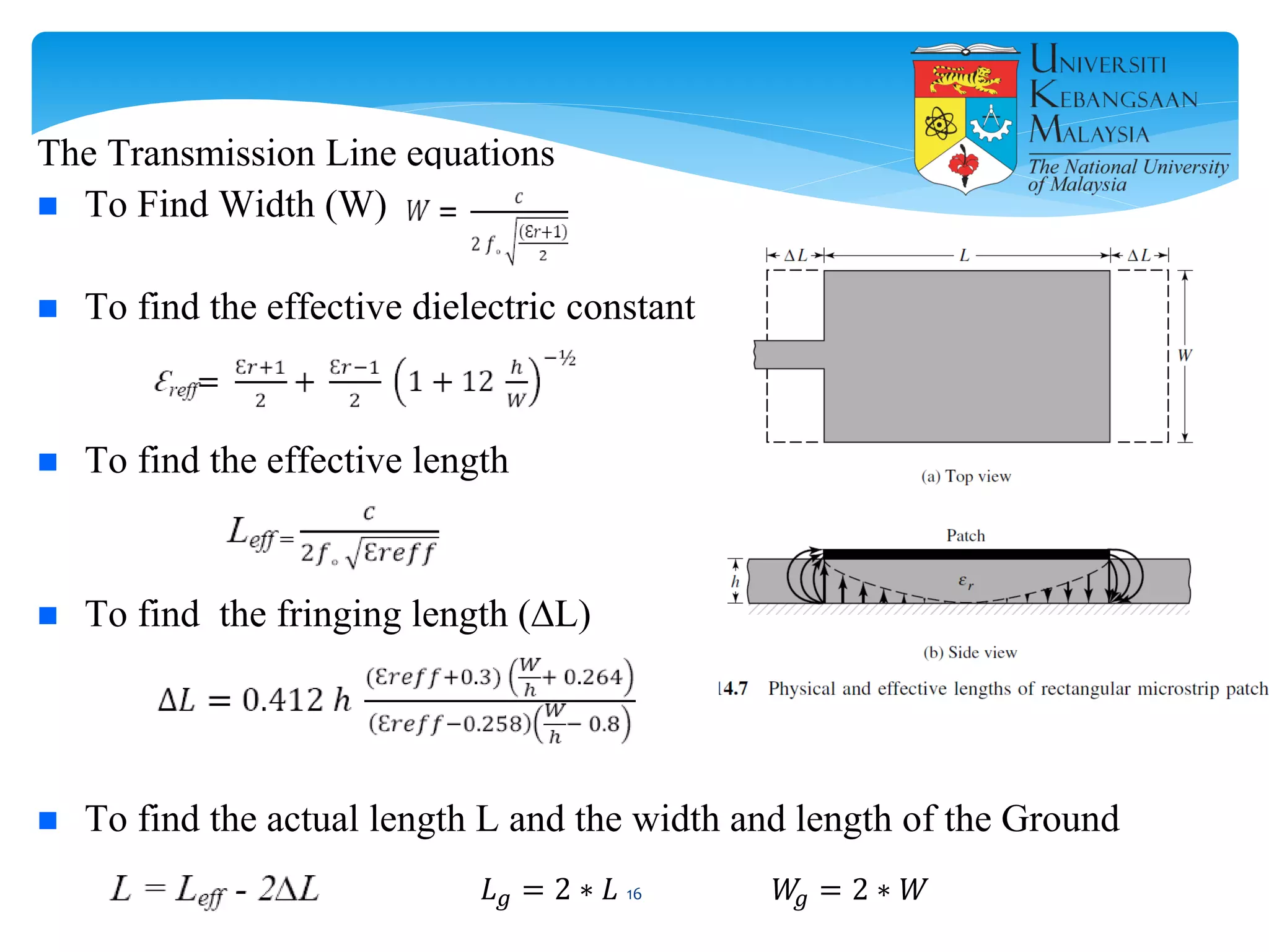
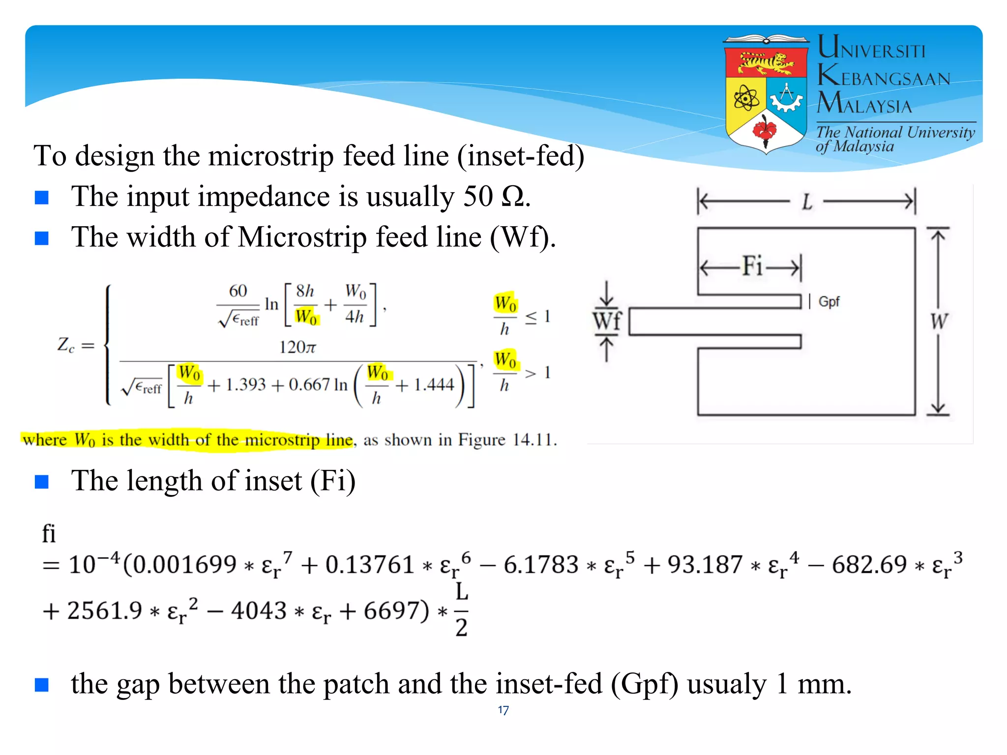
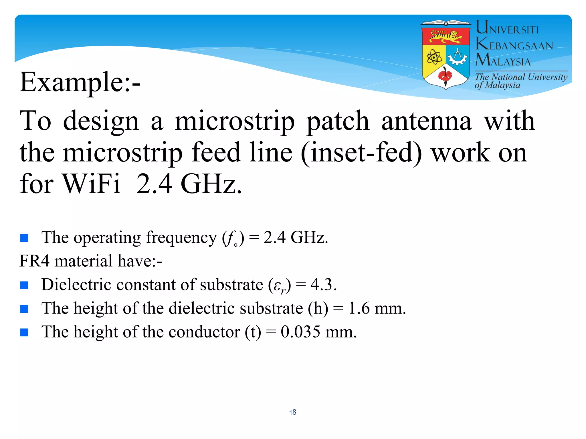
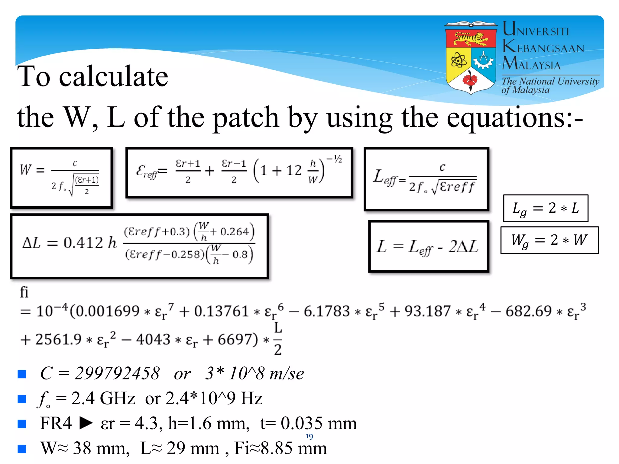
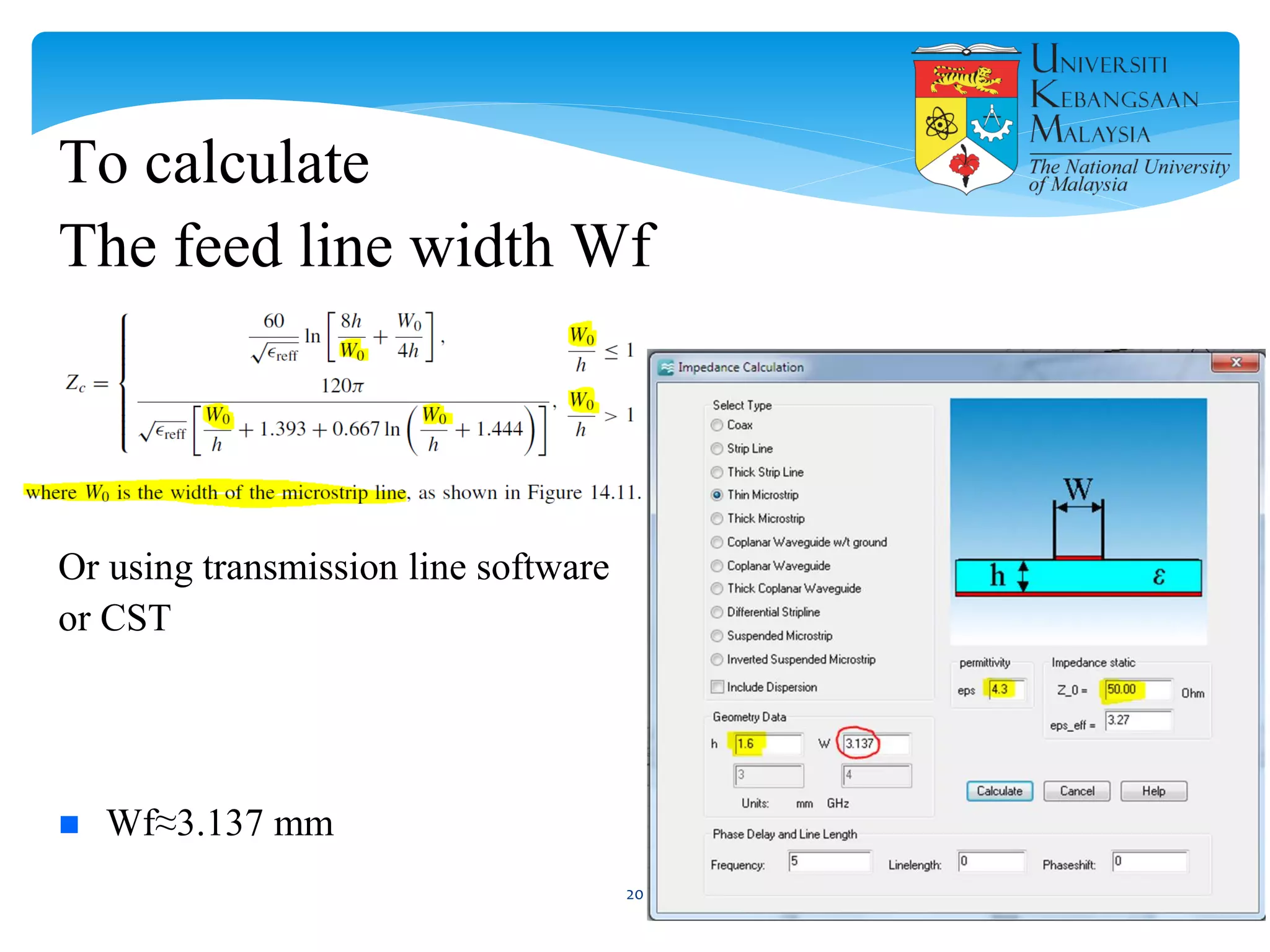
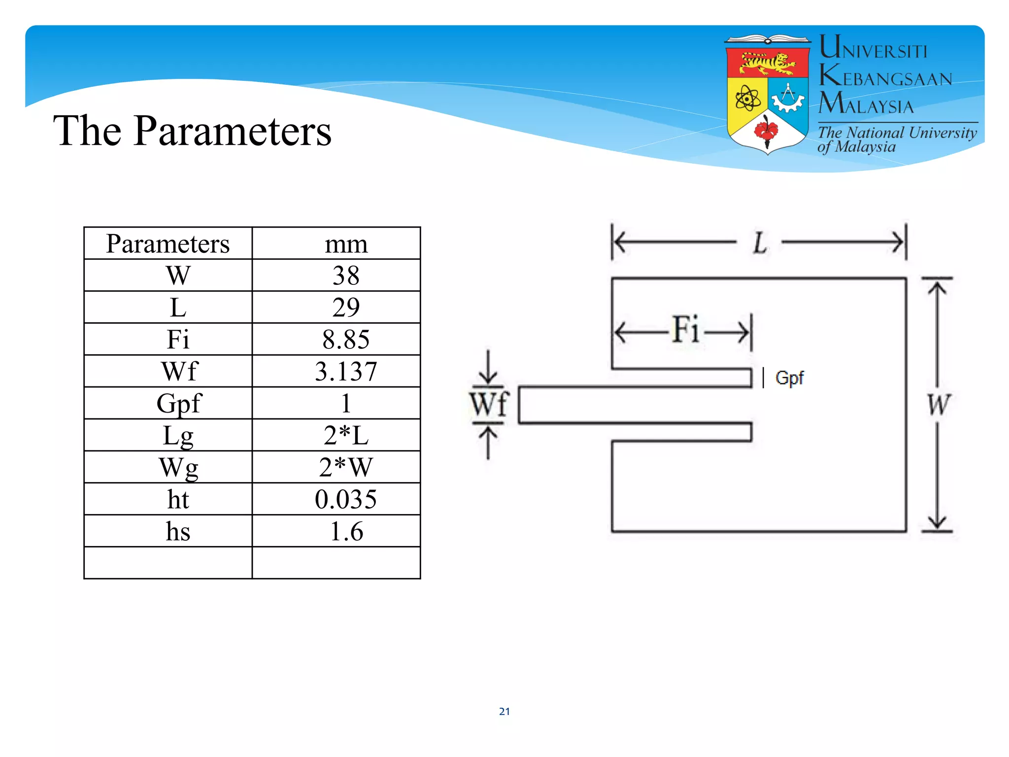

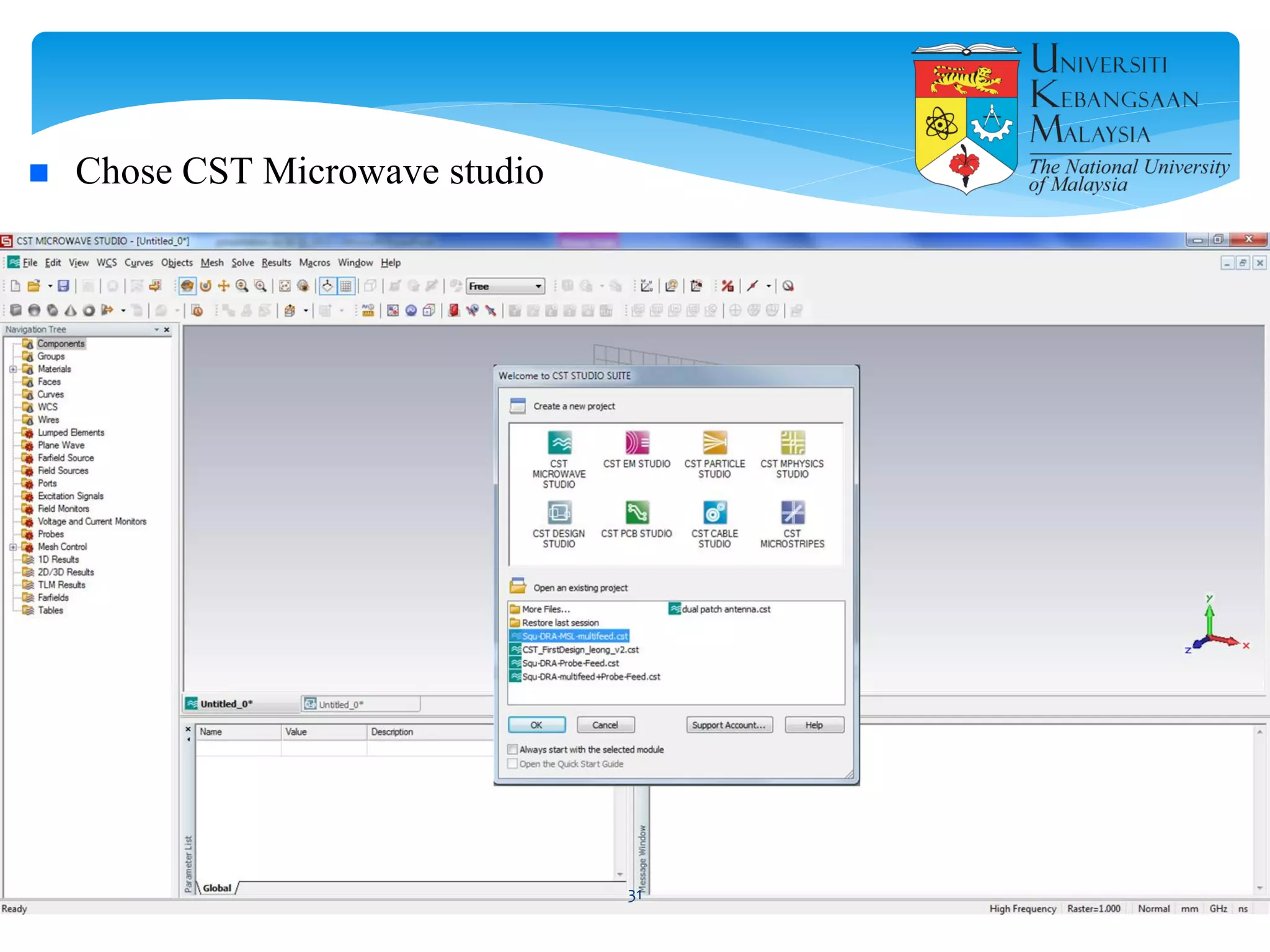
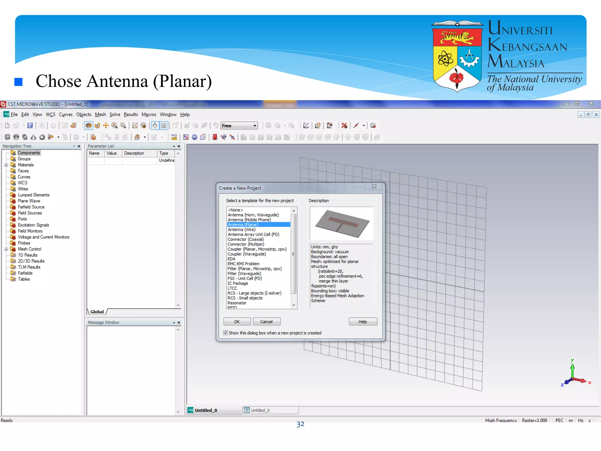
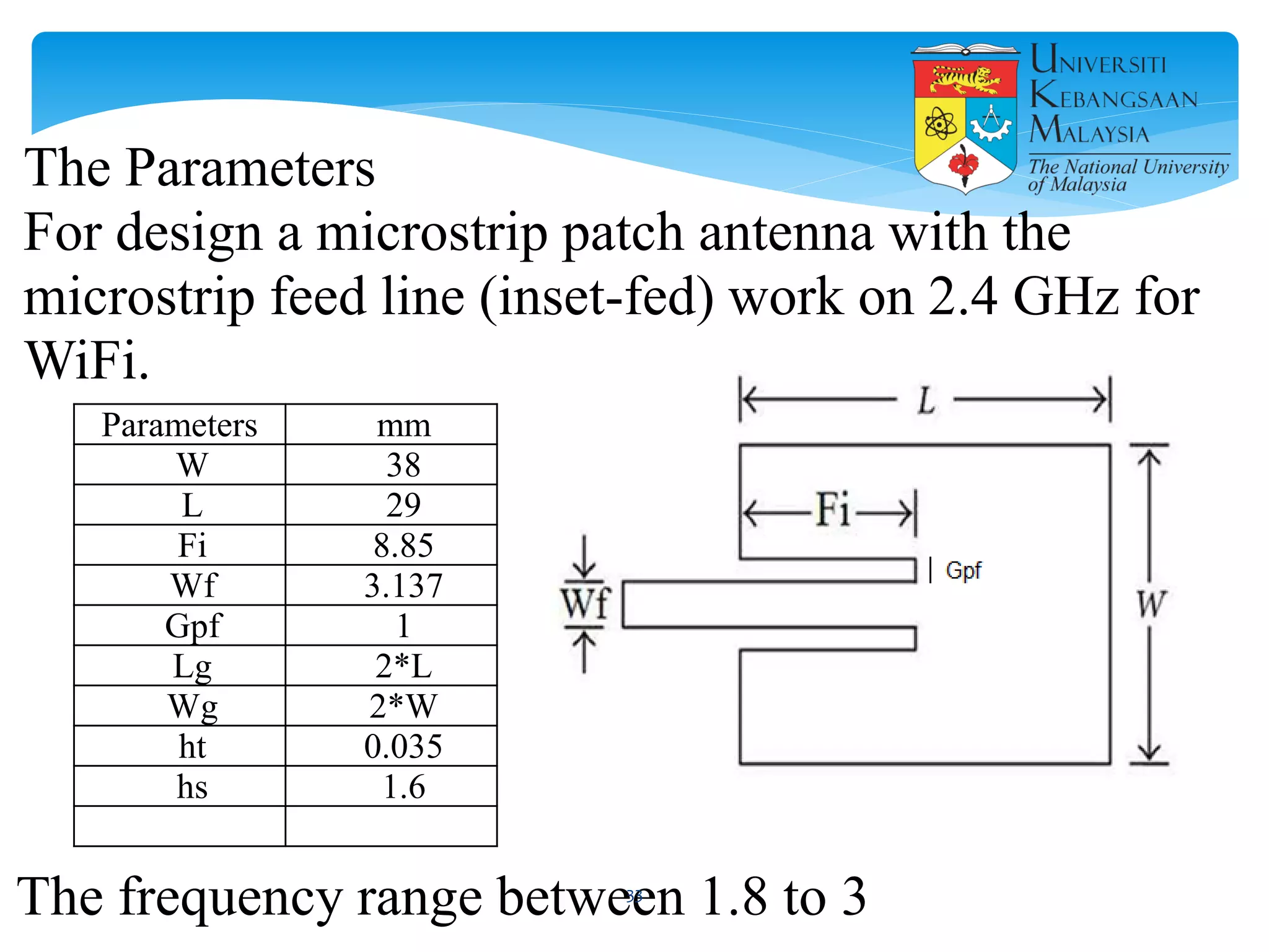
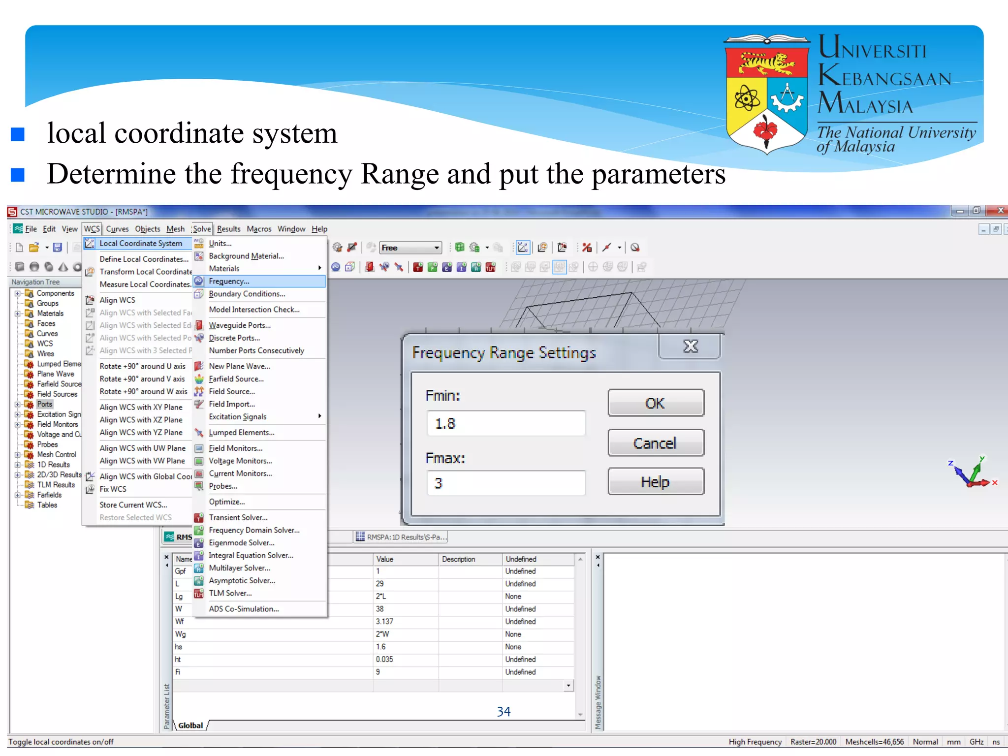
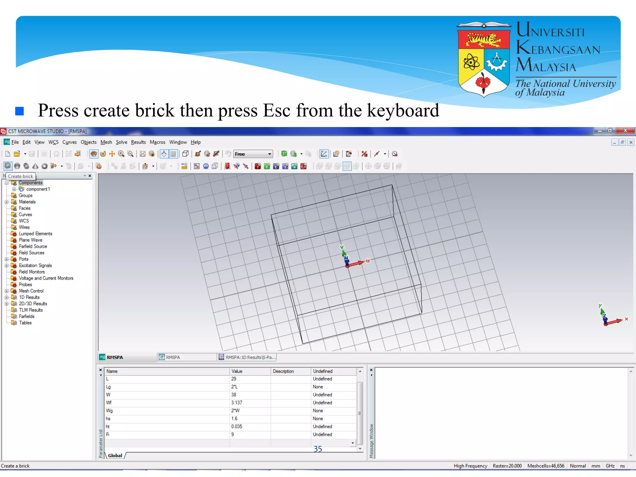
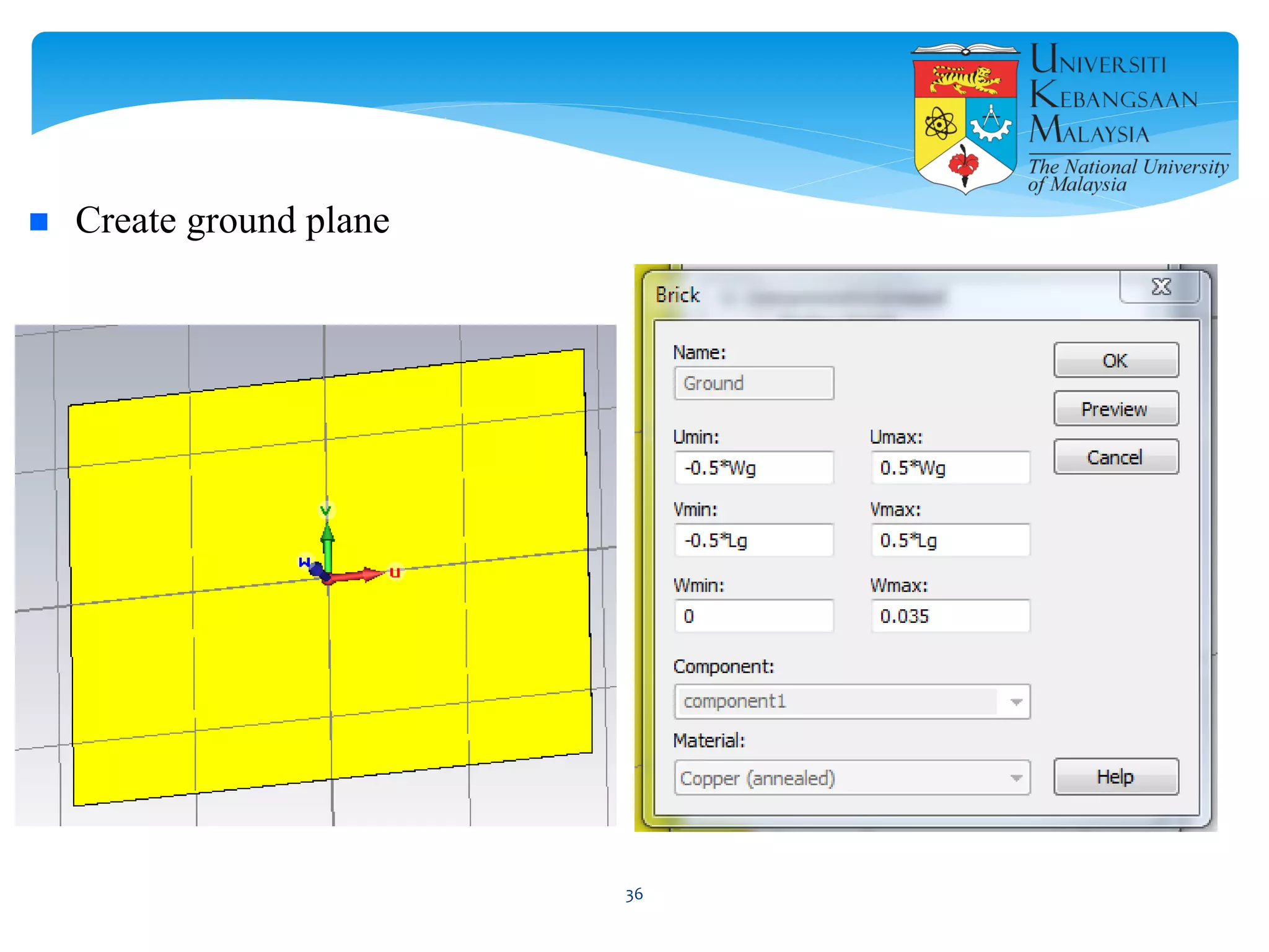
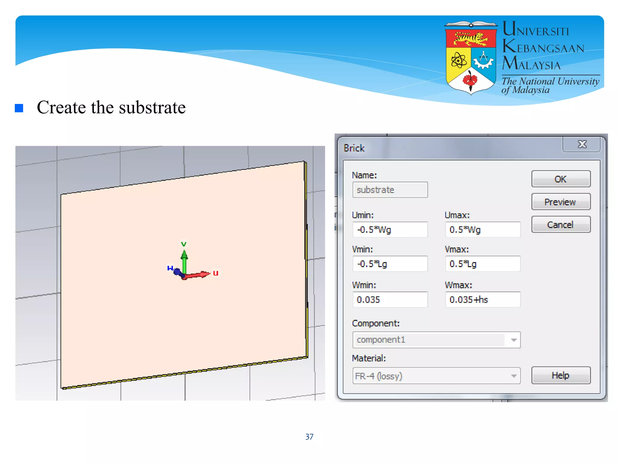
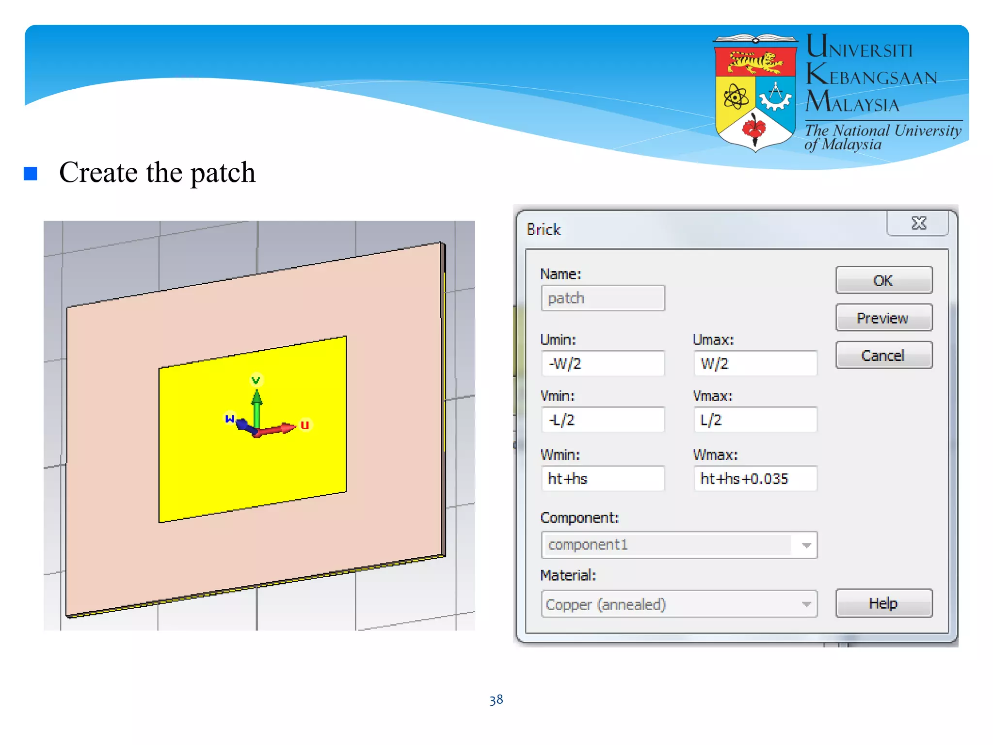
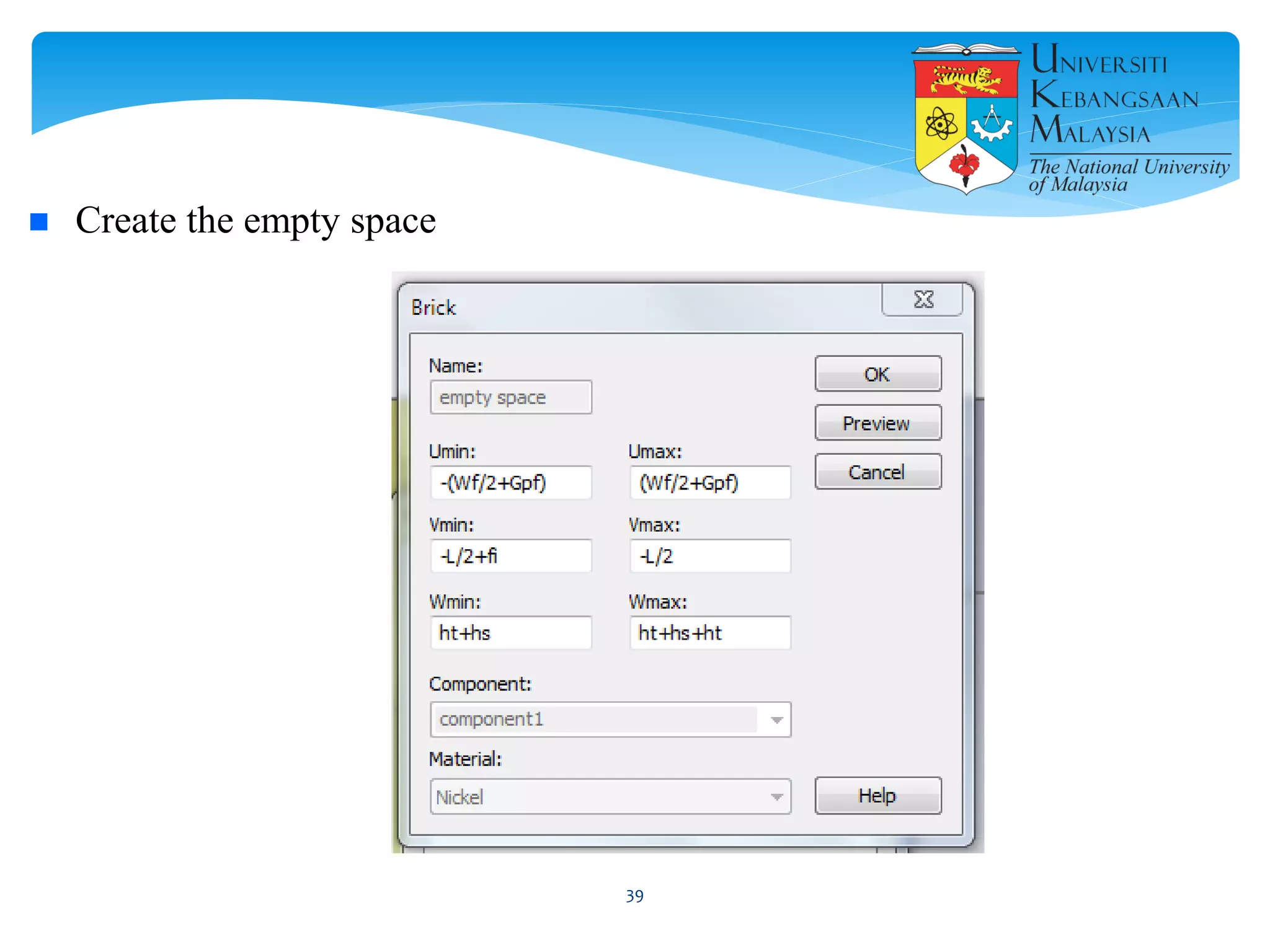
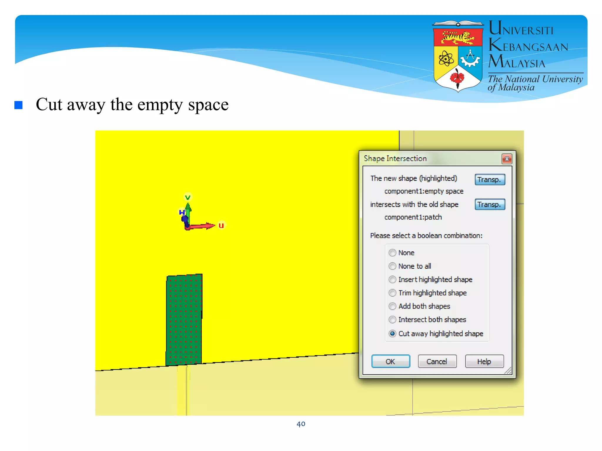
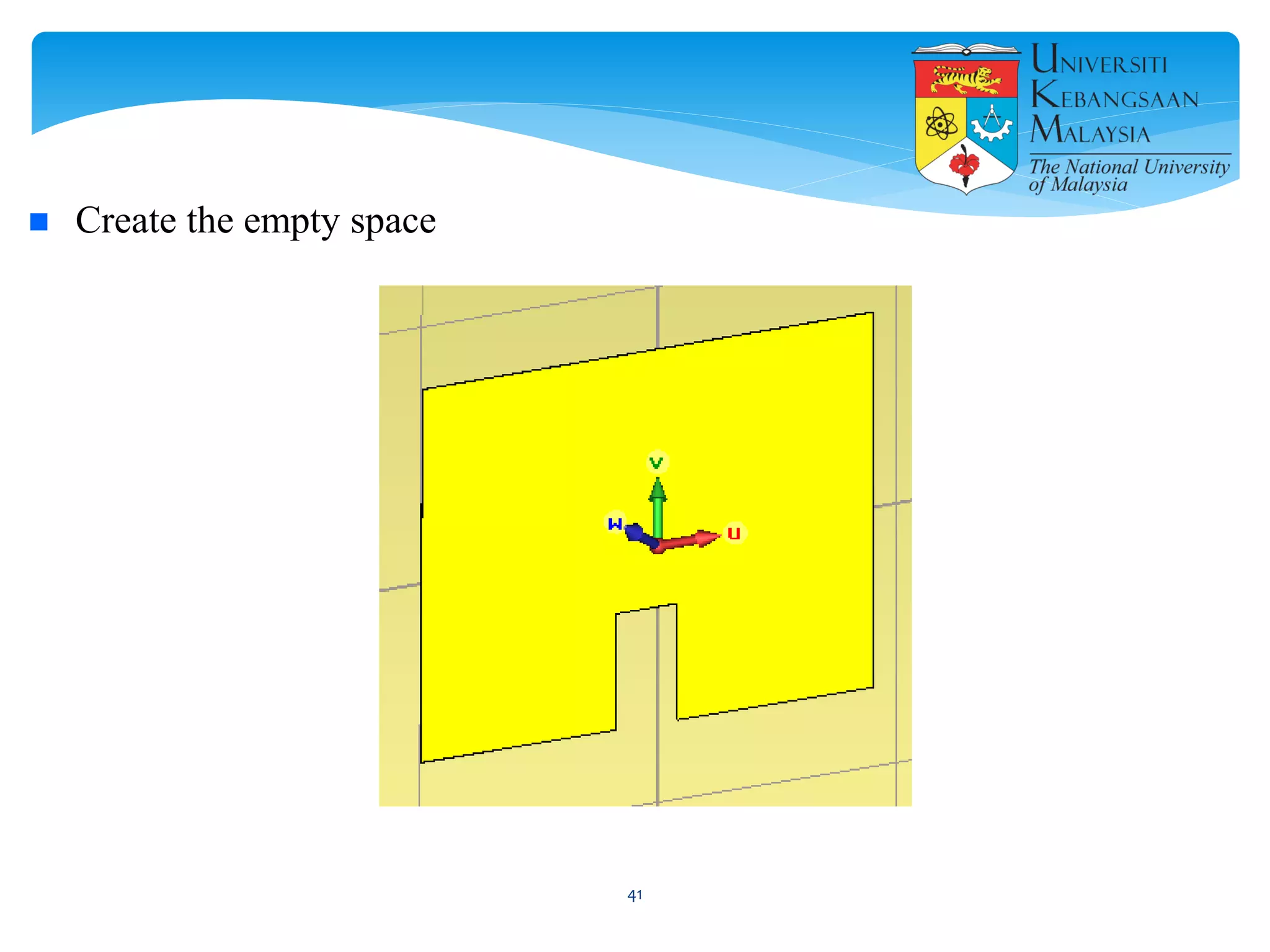
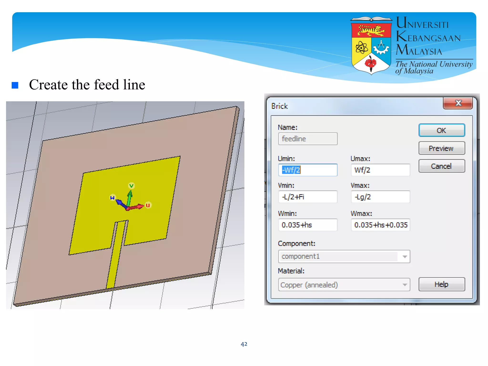
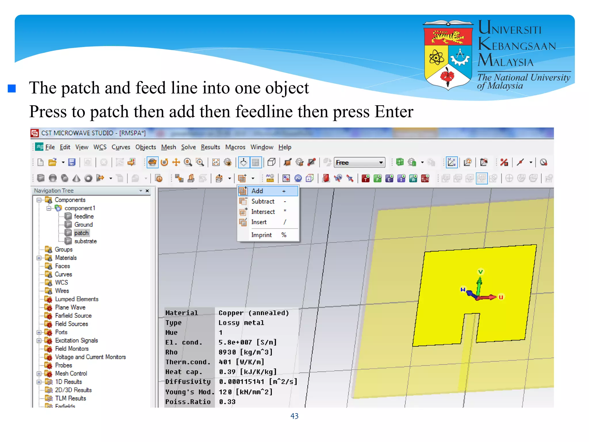
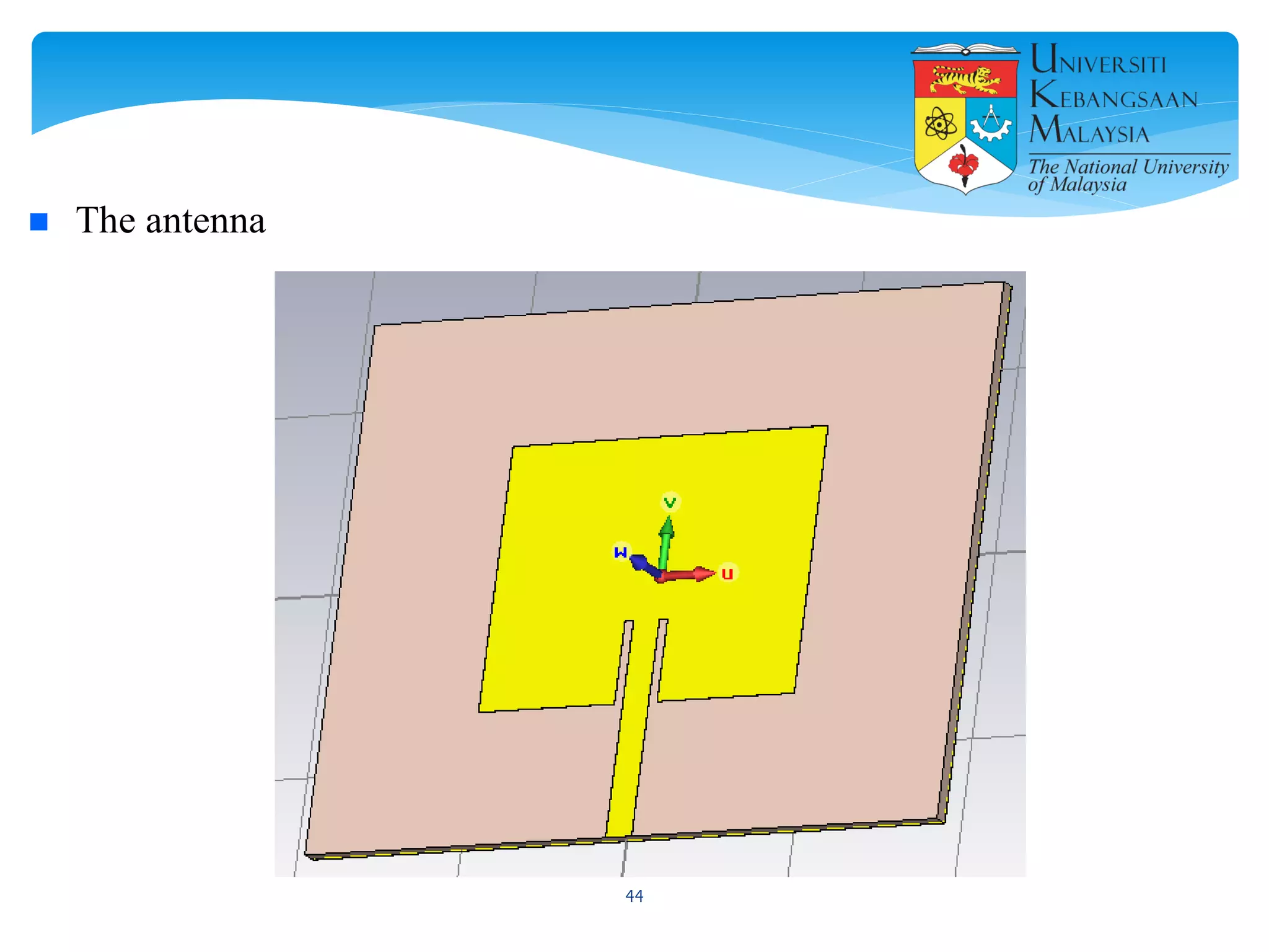
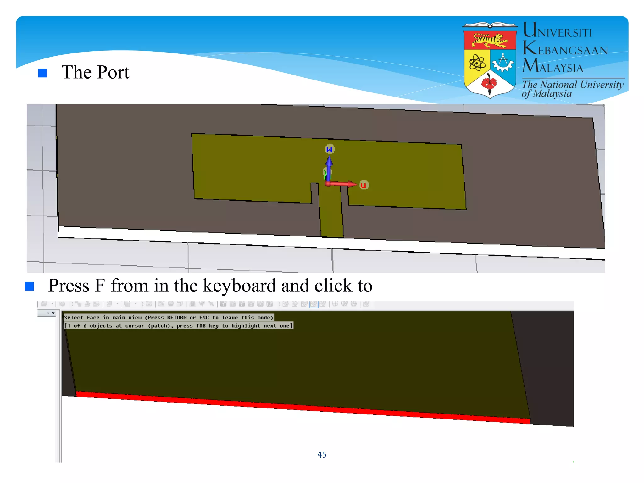

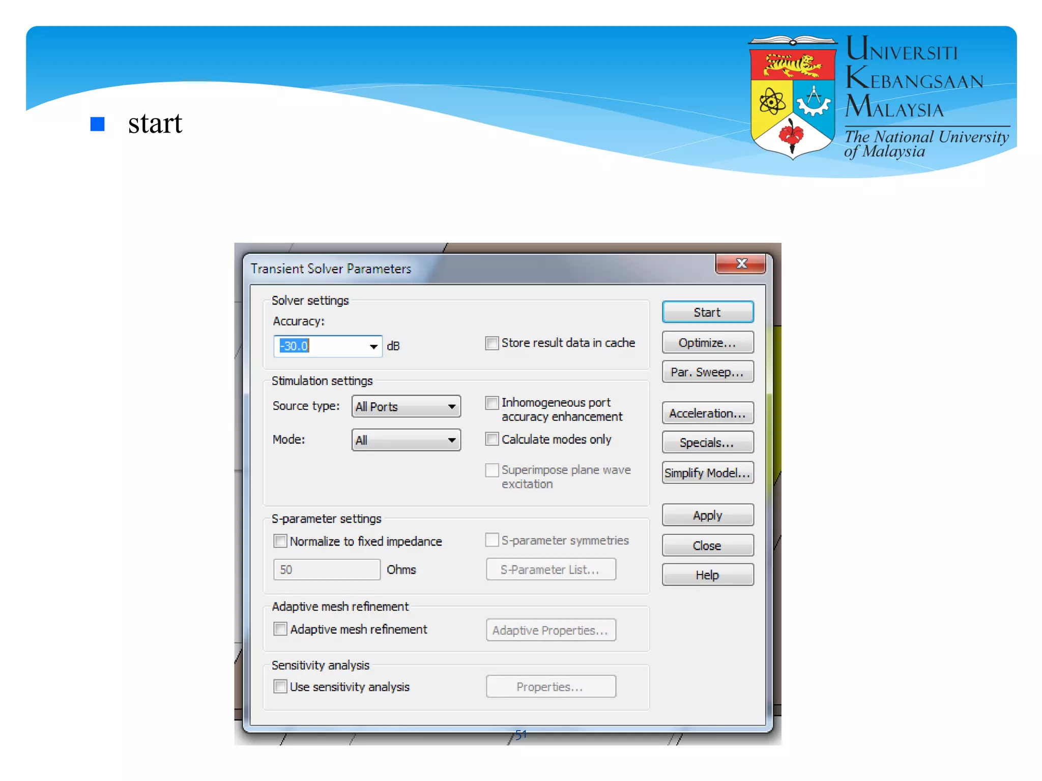
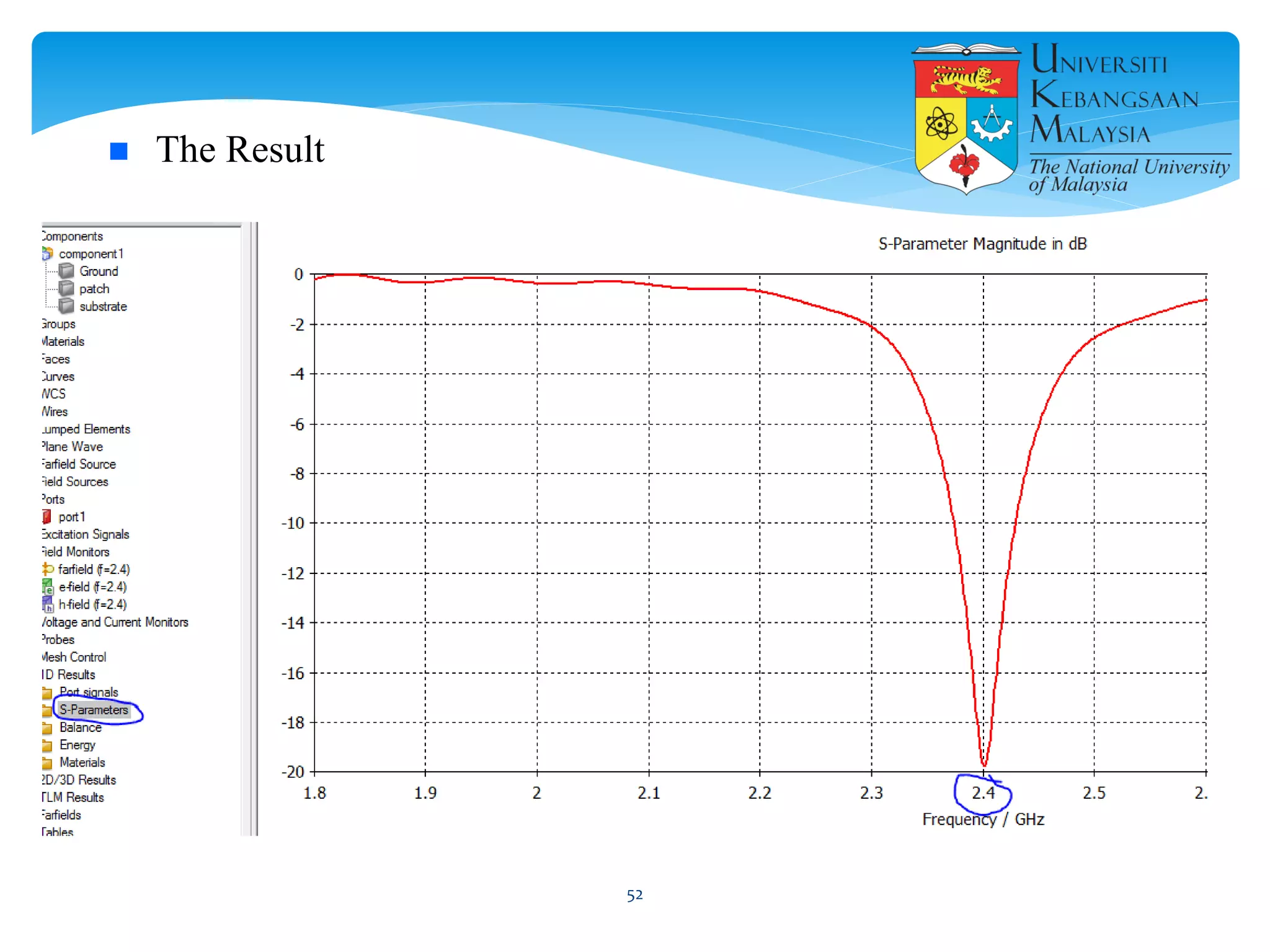
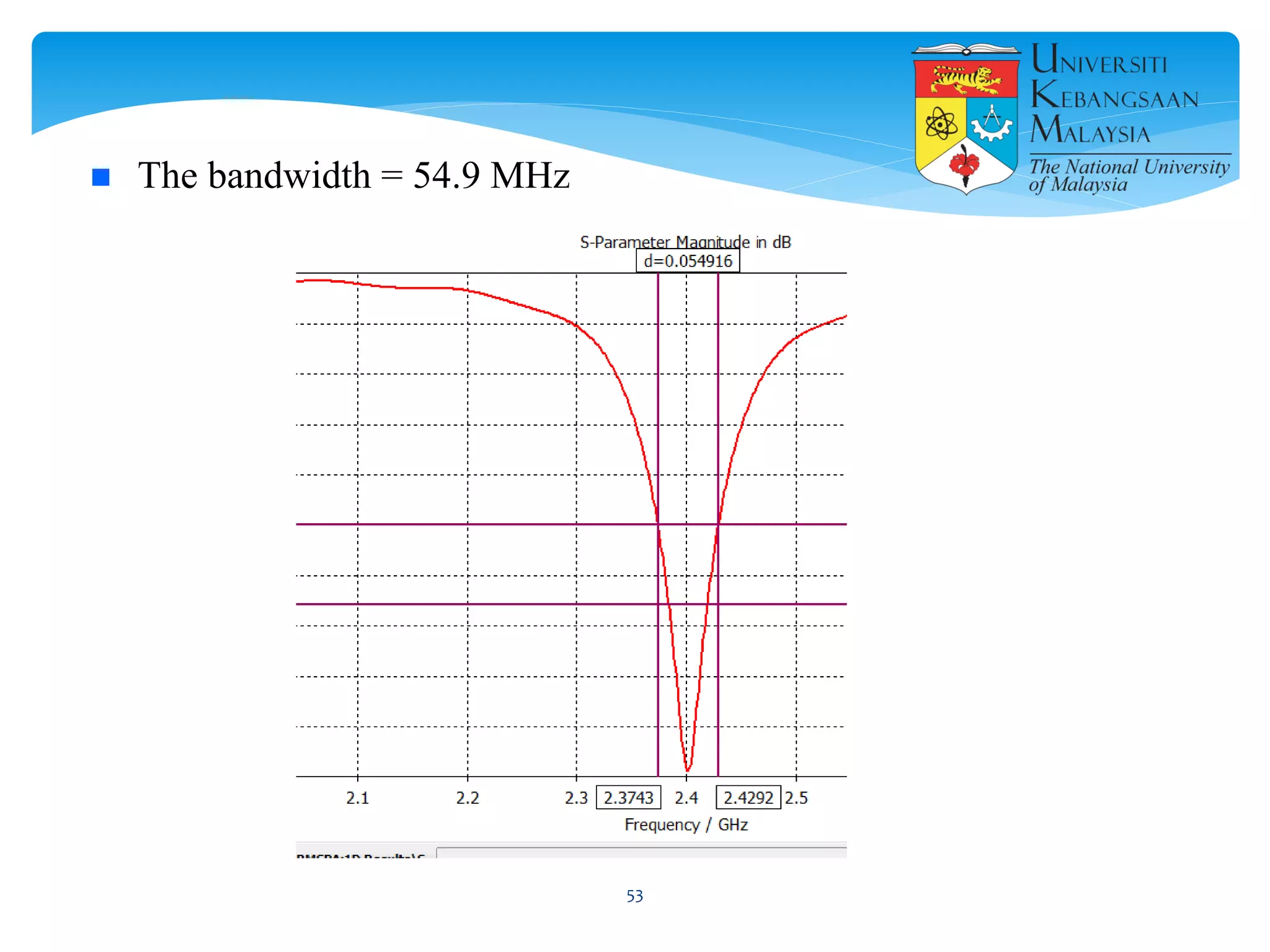
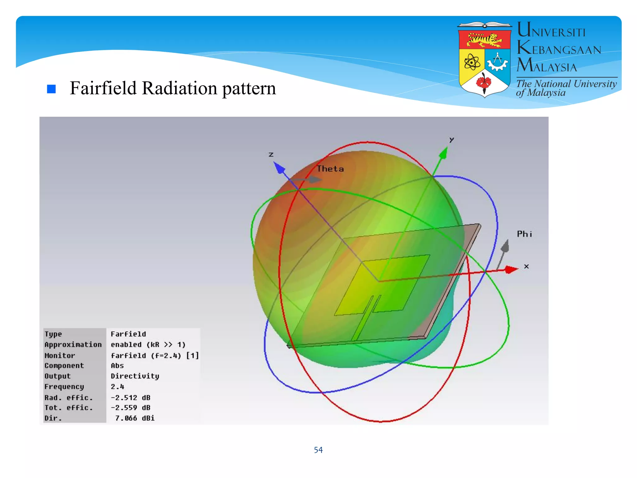


The document describes the design and simulation of a microstrip patch antenna in CST Microwave Studio. It begins with an introduction to microstrip patch antennas and their applications. Then, it outlines the theoretical design of a rectangular patch antenna for 2.4 GHz WiFi using transmission line equations. Finally, it details the simulation process in CST Microwave Studio, including adding the patch, feedline, substrate and ground plane, assigning materials and frequencies, setting up the port and monitors, and solving to obtain results like the bandwidth and radiation pattern.