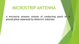
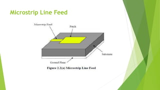
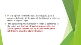
MICROSTRIP ANTENNA
Prepared by:
B.S.NageswaraRao
Assistant Professor
Department Of ECE
Eswar College Of Engineering
Narasaraopet
Andhra Pradesh.
MICROSTRIP ANTENNA
A microstrip antenna consists of conducting patch on a
ground plane separated by dielectric substrate.
 This concept was undeveloped until the revolution in
electronic circuit miniaturization and large-scale
integration in 1970.
 The early work of Munson on micro strip antennas for use as a
low profile flush mounted antennas on rockets and missiles
 micro strip antennas are the present day antenna designer’s
choice.
Low dielectric constant substrates are generally preferred for
maximum radiation.
 conducting patch can take any shape but rectangular and circular
configurations are the most commonly used configuration.
 Other configurations are complex to analyze and require heavy
numerical computations
 Some of the principal advantages of microstrip antennas compared
to conventional antennas are:
Light wieght,low volume and thin profile configuration, which can
be made conformal.
Low fabrication cost,reily amenable to mass production.
Linear and circular polarization antennas can be easily made.
 Can be easily integrated with microwave integrated circuits.
Feed lines and matching networks can be fabricated
simultaneously with the antenna structure.
 microstrip antennas also have some limitations compared to
conventional microwave Antenna
 Narrow bandwidth and associated tolerance problems.
 Somewhat lower gain(-6dB).
 Large ohmic loss in the feed structure of arrays.
Most microstrip antennas radiate into half space.
Complex feed structures required for high performance
arrays.
Polarization purity is difficult to achieve.
Low power handling capability(~100W)
Excitation of surface waves.
Reduced gain and efficiency as well as unacceptably high
levels of cross polarization and mutual coupling within an
array environment at high frequencies.
 Microstrip antennas are attractive due to their light
weight, conformability and low cost. These antennas can
be integrated with printed strip-line feed networks and
active devices.
 This is a relatively new area of antenna engineering.
 The radiation properties of micro strip structures have
been known since the mid 1950’s.
 The application of this type of antennas started in early
1970’s when conformal antennas were required for
missiles.
 Rectangular and circular micro strip resonant patches
have been used extensively in a variety of array
configurations.
 In its most fundamental form, a Microstrip Patch antenna consists of
a radiating patch on one side of a dielectric substrate which has a
ground plane on the other side as shown in Figure
 The patch is generally made of conducting
material such as copper or gold and can take any
possible shape.
 The radiating patch and the feed lines are usually
photo etched on the dielectric substrate
the patch is generally
 square,
 rectangular,
 circular,
 triangular,
 and elliptical or some other common shape as shown in
figure
 For a rectangular patch, the length L of the patch is usually
0.3333λo< L < 0.5 λo, where λo is the free-space wavelength.
 The patch is selected to be very thin such that t << λo (where
t is the patch thickness).
 The height h of the dielectric substrate is usually 0.003
λo≤h≤0.05 λo. The dielectric constant of the substrate (εr) is
typically in the range 2.2 ≤ εr≤ 12.
 Microstrip patch antennas radiate primarily because of the
fringing fields between the patch edge and the ground plane.
 For good antenna performance, a thick dielectric substrate
having a low dielectric constant is desirable since this provides
better efficiency, larger bandwidth and better radiation.
 However, such a configuration leads to a larger antenna size. In
order to design a compact Microstrip patch antenna, substrates with
higher dielectric constants must be used which are less efficient
and result in narrower bandwidth.
 Hence a trade-off must be realized between the antenna
dimensions and antenna performance.
Properties of a Basic Microstrip Patch
 A microstrip or patch antenna is a low profile antenna that has a
number of advantages over other antennas it is lightweight,
inexpensive, and easy to integrate with accompanying
electronics.
 the elements are usually flat; hence their other name, planar
antennas. Note that a planar antenna is not always a patch
antenna.
Feed Techniques
 Microstrip patch antennas can be fed by a variety of
methods.
 These methods can be classified into two categories-
contacting and non-contacting.
 In the contacting method, the RF power is fed directly to
the radiating patch using a connecting element
such as a microstrip line.
 In the non-contacting scheme
electromagnetic field coupling is done to transfer power between
the microstrip line and the radiating patch.
The four most popular feed techniques used are
 the microstrip line, coaxial probe (both contacting
schemes),
 aperture coupling and proximity coupling (both non-
contacting schemes).
Microstrip Line Feed
 In this type of feed technique, a conducting strip is
connected directly to the edge of the Microstrip patch as
shown in Figure 2.2(a).
 The conducting strip is smaller in width as compared to
the patch and this kind of feed arrangement has the
advantage that the feed can be etched on the same
substrate to provide a planar structure.
 The purpose of the inset cut in the patch is to match the
impedance of the feed line to the patch without the need
for any additional matching element.
 This is achieved by properly controlling the inset position.
this is an easy feeding scheme,
 since it provides ease of fabrication and simplicity in
modeling as well as impedance matching.
 However as the thickness of the dielectric substrate being
used, increases, surface waves and spurious feed radiation
also increases, which hampers the bandwidth of the
antenna.
 The feed radiation also leads to undesired cross polarized
radiation.
Coaxial Feed
 The Coaxial feed or probe feed is a very common
technique used for feeding Microstrip patch antennas.
 As seen from Figure 2.2(b), the inner conductor of the
coaxial connector extends through the dielectric and is
soldered to the radiating patch, while the outer conductor
is connected to the ground plane.
 The main advantage of this type of feeding scheme is that
the feed can be placed at any desired location inside the
patch in order to match with its input impedance.
 This feed method is easy to fabricate and has low spurious
radiation. However, a
 major disadvantage is that it provides narrow bandwidth
and is difficult to model since a hole has to be drilled in
the substrate and the connector protrudes outside the
ground plane, thus not making it completely planar for
thick substrates (h > 0.02λo).
 For thicker substrates,
the increased probe length makes the input impedance more
inductive, leading to matching problems.
 the microstrip line feed and the coaxial feed suffer from
numerous disadvantages.
 The non-contacting feed techniques which have been
discussed below, solve these issues.
Aperture Coupled Feed
 In this type of feed technique, the radiating patch and the
microstrip feed line are separated by the ground plane as
shown in Figure 2.2(c).
 Coupling between the patch and the feed line is made
through a slot or an aperture in the ground plane.
 The coupling aperture is usually centered under the
patch, leading to lower cross polarization due to
symmetry of the configuration.
 The amount of coupling from the feed line to the patch is
determined by the shape, size and location of the
aperture.
 Since the ground plane separates the patch and the feed
line, spurious radiation is minimized.
 high dielectric material is used for bottom substrate and a thick,
low dielectric constant material is used for the top substrate to
optimize radiation from the patch.
The major disadvantage of this feed technique is that
 it is difficult to fabricate due to multiple layers, which
also increases the antenna thickness. This feeding scheme
also provides narrow bandwidth.
Proximity Coupled Feed
 feed technique is also called as the electromagnetic coupling scheme
 two dielectric substrates are used such that the feed line
is between the two substrates and the radiating patch is
on top of the upper substrate
 The main advantage of this feed technique is that it
eliminates spurious feed radiation and provides very high
bandwidth (as high as 13%), due to overall increase in the
thickness of the microstrip patch antenna
 The major disadvantage of this feed scheme is that it is
difficult to fabricate because of the two dielectric layers
which need proper alignment.
 Also, there is an increase in the overall thickness of the
antenna.
END

Microstrip antenna for awp class

  • 1.
    MICROSTRIP ANTENNA Prepared by: B.S.NageswaraRao AssistantProfessor Department Of ECE Eswar College Of Engineering Narasaraopet Andhra Pradesh.
  • 2.
    MICROSTRIP ANTENNA A microstripantenna consists of conducting patch on a ground plane separated by dielectric substrate.
  • 3.
     This conceptwas undeveloped until the revolution in electronic circuit miniaturization and large-scale integration in 1970.
  • 4.
     The earlywork of Munson on micro strip antennas for use as a low profile flush mounted antennas on rockets and missiles
  • 5.
     micro stripantennas are the present day antenna designer’s choice. Low dielectric constant substrates are generally preferred for maximum radiation.
  • 6.
     conducting patchcan take any shape but rectangular and circular configurations are the most commonly used configuration.  Other configurations are complex to analyze and require heavy numerical computations
  • 7.
     Some ofthe principal advantages of microstrip antennas compared to conventional antennas are: Light wieght,low volume and thin profile configuration, which can be made conformal. Low fabrication cost,reily amenable to mass production. Linear and circular polarization antennas can be easily made.
  • 8.
     Can beeasily integrated with microwave integrated circuits. Feed lines and matching networks can be fabricated simultaneously with the antenna structure.
  • 9.
     microstrip antennasalso have some limitations compared to conventional microwave Antenna  Narrow bandwidth and associated tolerance problems.  Somewhat lower gain(-6dB).  Large ohmic loss in the feed structure of arrays.
  • 10.
    Most microstrip antennasradiate into half space. Complex feed structures required for high performance arrays. Polarization purity is difficult to achieve. Low power handling capability(~100W) Excitation of surface waves. Reduced gain and efficiency as well as unacceptably high levels of cross polarization and mutual coupling within an array environment at high frequencies.
  • 11.
     Microstrip antennasare attractive due to their light weight, conformability and low cost. These antennas can be integrated with printed strip-line feed networks and active devices.
  • 12.
     This isa relatively new area of antenna engineering.
  • 13.
     The radiationproperties of micro strip structures have been known since the mid 1950’s.  The application of this type of antennas started in early 1970’s when conformal antennas were required for missiles.  Rectangular and circular micro strip resonant patches have been used extensively in a variety of array configurations.
  • 15.
     In itsmost fundamental form, a Microstrip Patch antenna consists of a radiating patch on one side of a dielectric substrate which has a ground plane on the other side as shown in Figure
  • 16.
     The patchis generally made of conducting material such as copper or gold and can take any possible shape.  The radiating patch and the feed lines are usually photo etched on the dielectric substrate
  • 17.
    the patch isgenerally  square,  rectangular,  circular,  triangular,  and elliptical or some other common shape as shown in figure
  • 19.
     For arectangular patch, the length L of the patch is usually 0.3333λo< L < 0.5 λo, where λo is the free-space wavelength.  The patch is selected to be very thin such that t << λo (where t is the patch thickness).  The height h of the dielectric substrate is usually 0.003 λo≤h≤0.05 λo. The dielectric constant of the substrate (εr) is typically in the range 2.2 ≤ εr≤ 12.
  • 20.
     Microstrip patchantennas radiate primarily because of the fringing fields between the patch edge and the ground plane.  For good antenna performance, a thick dielectric substrate having a low dielectric constant is desirable since this provides better efficiency, larger bandwidth and better radiation.
  • 21.
     However, sucha configuration leads to a larger antenna size. In order to design a compact Microstrip patch antenna, substrates with higher dielectric constants must be used which are less efficient and result in narrower bandwidth.  Hence a trade-off must be realized between the antenna dimensions and antenna performance.
  • 22.
    Properties of aBasic Microstrip Patch  A microstrip or patch antenna is a low profile antenna that has a number of advantages over other antennas it is lightweight, inexpensive, and easy to integrate with accompanying electronics.  the elements are usually flat; hence their other name, planar antennas. Note that a planar antenna is not always a patch antenna.
  • 23.
    Feed Techniques  Microstrippatch antennas can be fed by a variety of methods.  These methods can be classified into two categories- contacting and non-contacting.
  • 24.
     In thecontacting method, the RF power is fed directly to the radiating patch using a connecting element such as a microstrip line.
  • 25.
     In thenon-contacting scheme electromagnetic field coupling is done to transfer power between the microstrip line and the radiating patch.
  • 26.
    The four mostpopular feed techniques used are  the microstrip line, coaxial probe (both contacting schemes),  aperture coupling and proximity coupling (both non- contacting schemes).
  • 27.
  • 28.
     In thistype of feed technique, a conducting strip is connected directly to the edge of the Microstrip patch as shown in Figure 2.2(a).  The conducting strip is smaller in width as compared to the patch and this kind of feed arrangement has the advantage that the feed can be etched on the same substrate to provide a planar structure.
  • 29.
     The purposeof the inset cut in the patch is to match the impedance of the feed line to the patch without the need for any additional matching element.  This is achieved by properly controlling the inset position.
  • 30.
    this is aneasy feeding scheme,  since it provides ease of fabrication and simplicity in modeling as well as impedance matching.  However as the thickness of the dielectric substrate being used, increases, surface waves and spurious feed radiation also increases, which hampers the bandwidth of the antenna.  The feed radiation also leads to undesired cross polarized radiation.
  • 31.
  • 32.
     The Coaxialfeed or probe feed is a very common technique used for feeding Microstrip patch antennas.  As seen from Figure 2.2(b), the inner conductor of the coaxial connector extends through the dielectric and is soldered to the radiating patch, while the outer conductor is connected to the ground plane.
  • 33.
     The mainadvantage of this type of feeding scheme is that the feed can be placed at any desired location inside the patch in order to match with its input impedance.
  • 34.
     This feedmethod is easy to fabricate and has low spurious radiation. However, a  major disadvantage is that it provides narrow bandwidth and is difficult to model since a hole has to be drilled in the substrate and the connector protrudes outside the ground plane, thus not making it completely planar for thick substrates (h > 0.02λo).
  • 35.
     For thickersubstrates, the increased probe length makes the input impedance more inductive, leading to matching problems.
  • 36.
     the microstripline feed and the coaxial feed suffer from numerous disadvantages.  The non-contacting feed techniques which have been discussed below, solve these issues.
  • 37.
  • 38.
     In thistype of feed technique, the radiating patch and the microstrip feed line are separated by the ground plane as shown in Figure 2.2(c).  Coupling between the patch and the feed line is made through a slot or an aperture in the ground plane.
  • 39.
     The couplingaperture is usually centered under the patch, leading to lower cross polarization due to symmetry of the configuration.  The amount of coupling from the feed line to the patch is determined by the shape, size and location of the aperture.  Since the ground plane separates the patch and the feed line, spurious radiation is minimized.
  • 40.
     high dielectricmaterial is used for bottom substrate and a thick, low dielectric constant material is used for the top substrate to optimize radiation from the patch.
  • 41.
    The major disadvantageof this feed technique is that  it is difficult to fabricate due to multiple layers, which also increases the antenna thickness. This feeding scheme also provides narrow bandwidth.
  • 42.
    Proximity Coupled Feed feed technique is also called as the electromagnetic coupling scheme
  • 43.
     two dielectricsubstrates are used such that the feed line is between the two substrates and the radiating patch is on top of the upper substrate  The main advantage of this feed technique is that it eliminates spurious feed radiation and provides very high bandwidth (as high as 13%), due to overall increase in the thickness of the microstrip patch antenna
  • 44.
     The majordisadvantage of this feed scheme is that it is difficult to fabricate because of the two dielectric layers which need proper alignment.  Also, there is an increase in the overall thickness of the antenna.
  • 45.