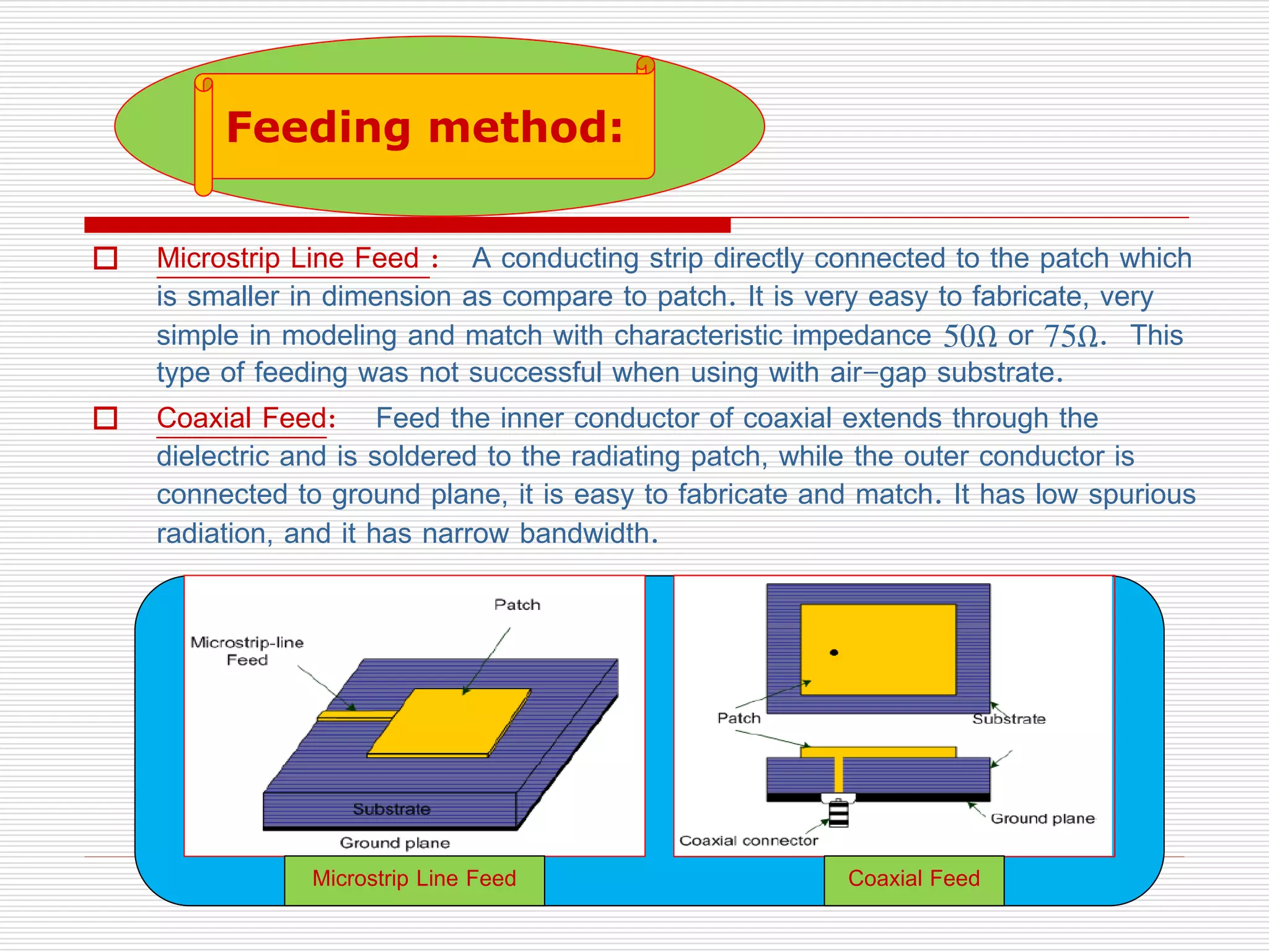
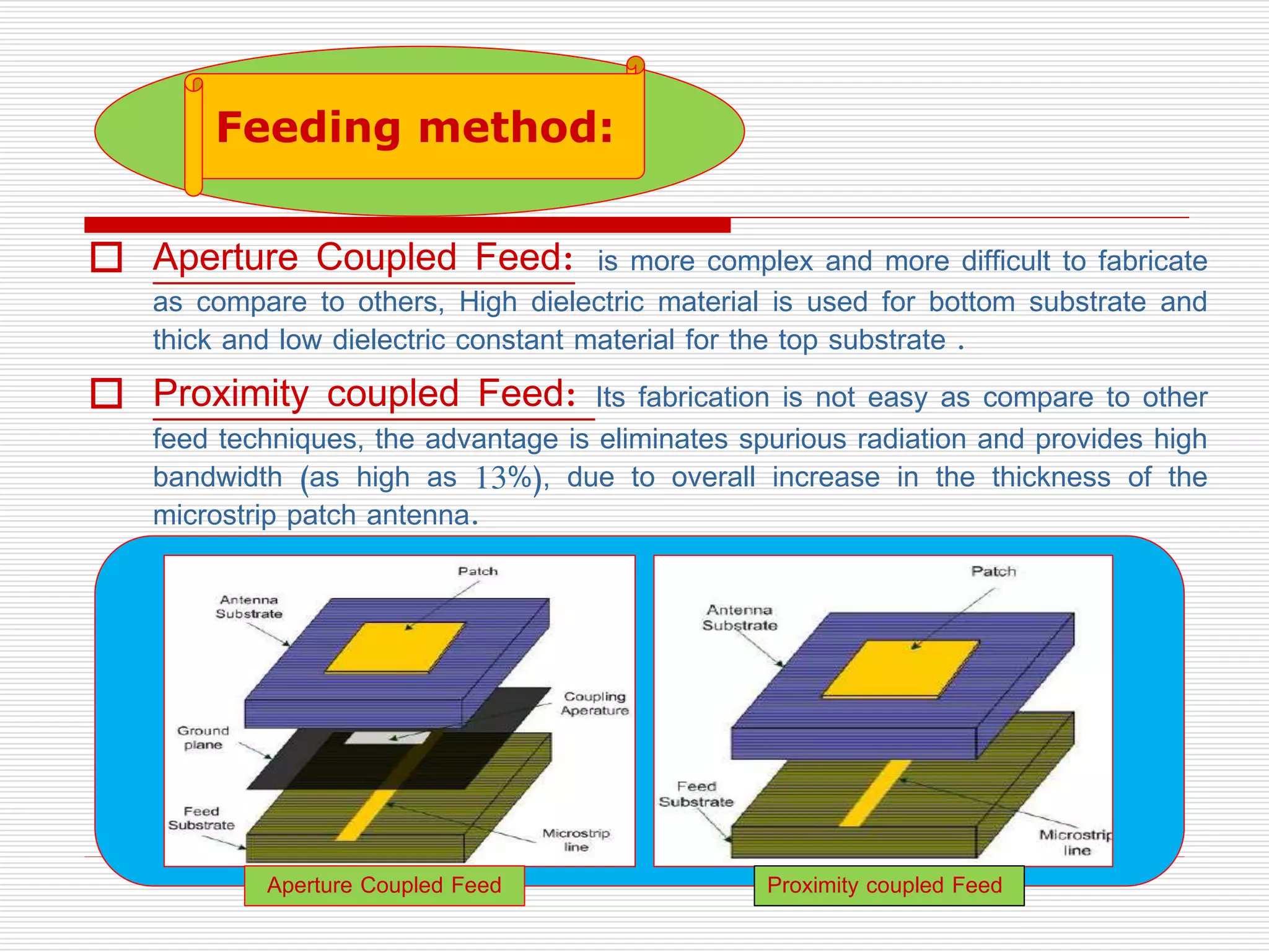
Downloaded 967 times


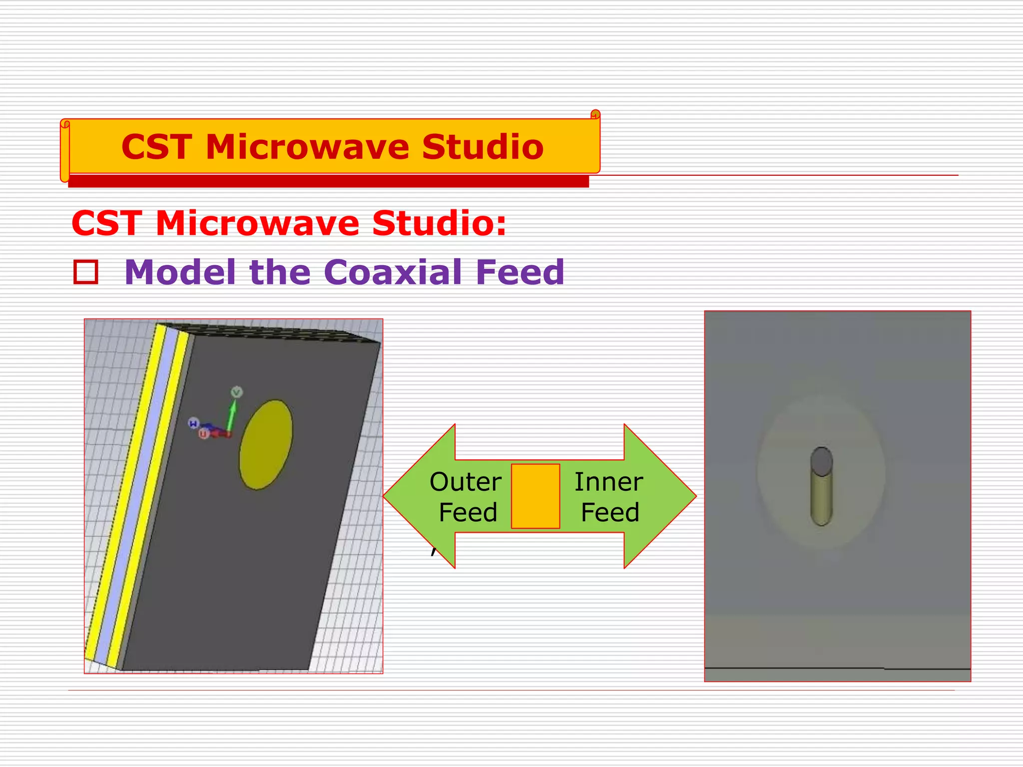
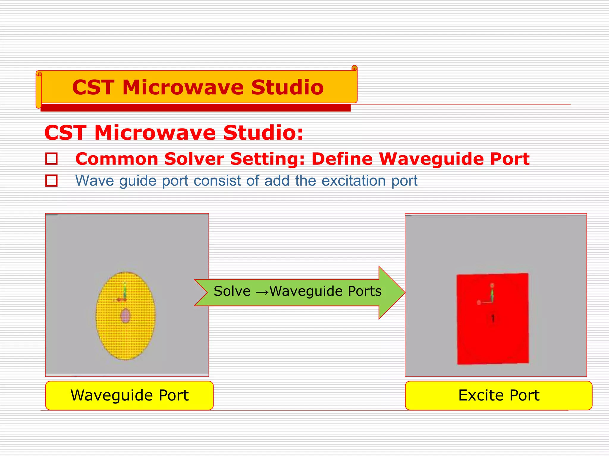
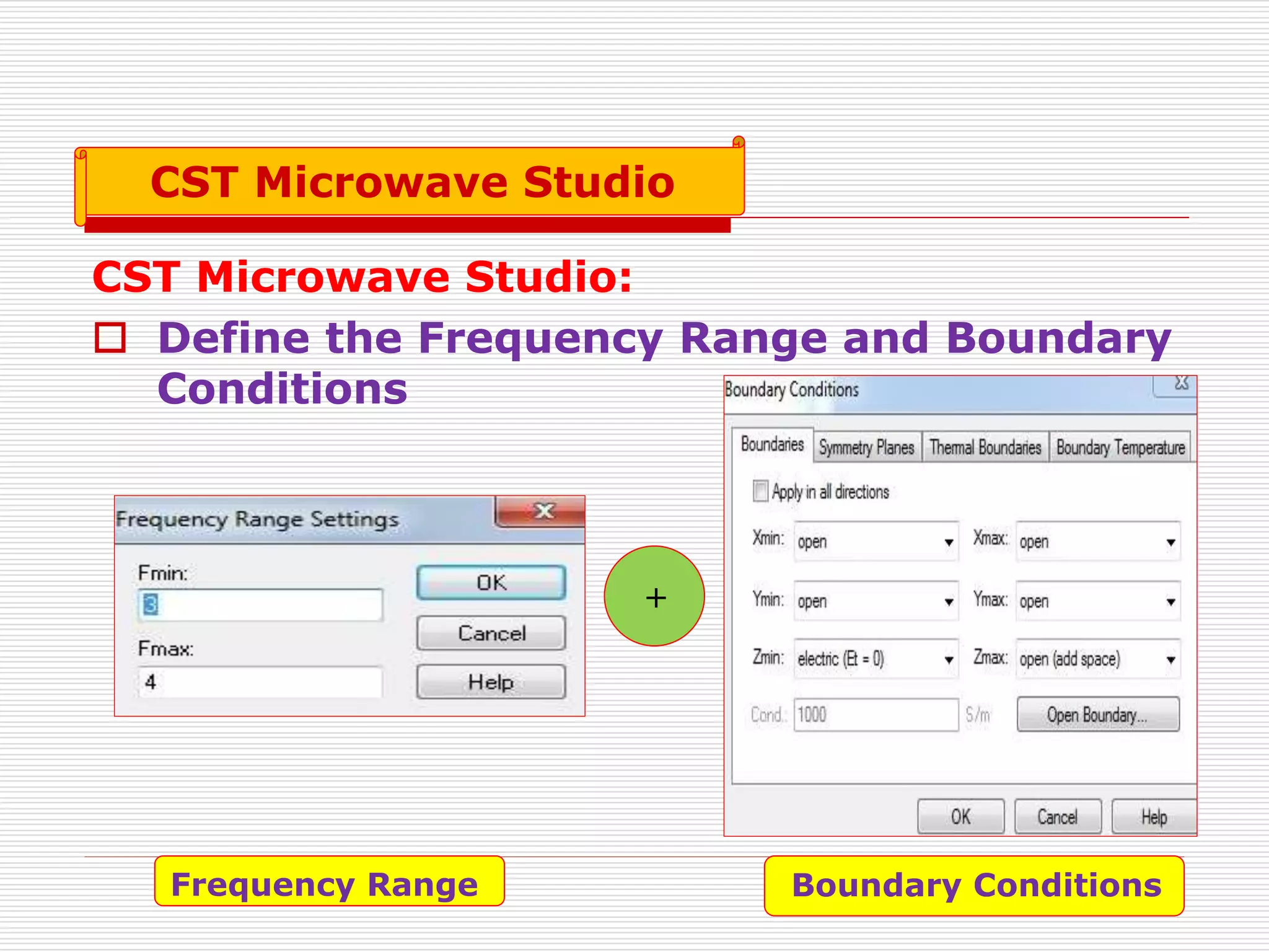
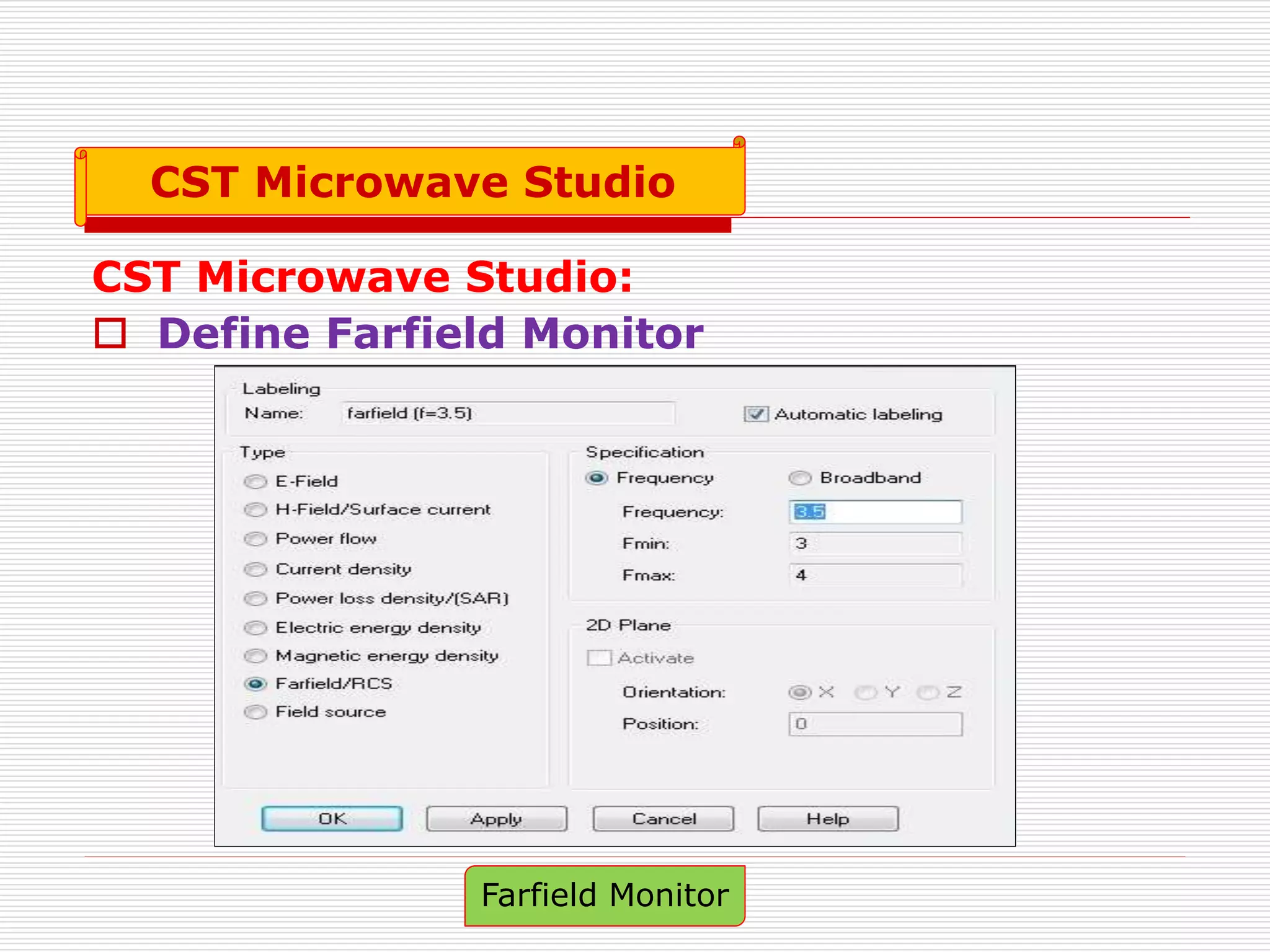

Waveguide Port CST Microwave Studio CST Microwave Studio: Mesh Setting: Define Mesh Mesh is the process of dividing the structure into small elements called cells or elements. Mesh Setting CST Microwave Studio CST Microwave Studio: Simulation Setting: Define Frequency Domain Solver Frequency Domain Solver is used to solve electromagnetic problems in the frequency domain. Frequency Domain Solver CST Microwave Studio