Downloaded 10 times
![Proceedings of the International Conference on Emerging Trends in
Because this technology is new it carries new challenges, including:
• Yield: Each extra manufacturing step adds a risk for defects.
• Heat: Simulations show that a 10°C raise in temperature can double a 3D IC chip’s heat density, degrading
performance by more than one-
issue as electrical proximity correlates
managed.
• Design complexity: Taking full advantage of 3D integration requires sophisticated design techniques and new
CAD tools.
3D IC integration technology is recent in IC
problem in 3D IC technology. Various techniques are introduced to mitigate heat dissipated in different IC layers. They
are classified as active and passive cooling techniques. Many shortco
active method of cooling, which uses peltier element to mitigate heat.
2. LITERATURE SURVEY
Sungjun et al[1] showed by Full Chip Thermal Analysis of Planar (2
Performance ICs [1] showed that interconnect Joule heating in advanced technology nodes can strongly impact the
magnitude of the maximum temperature within 2
thermal analysis of vertically integrated (3
simulations. Full chip thermal analysis of 2
numerical simulations shown that thermal de
considered during their early design phase. It has also been shown that interconnect Joule heating and low thermal
conductivity of dielectric materials will strongly impact the magn
with significant implications for reliability and performance.
Arifur Rahman et al [2] examined thermal issues in 3
analytical and numerical modeling of device
comparable system performance in 2-D and 3
integration due to lower capacitance associated with interconnec
ICs is higher (compared to that of 2-D ICs), chip temperature could reach an unacceptable level. The chip temperature is
generally limited by the heat removal capability of the packaging technology. T
for reliable operation of devices and interconnects, innovative package
Thermal vias, Cu bonding layer for 3-D integration, etc. could also be beneficial for heat remova
2.1. PASSIVE METHODS OF COOLI
2.1.1. INTER-TIER INTEGRATED M
Mohamed M. Sabry et al [3] proved that conventional back
cooling and micro channel cold-plates prove to
heat from multi-processor 3D ICs.
Fig1:
Inter-tier liquid cooling is a potential solution to address the high temperatures in 3D MPSoCs.
being developed by the CMOSAIC Nano
the tiers of a 3D stack. This cooling technology scales with
vertical interconnects (through silicon vias or TSVs), which are needed to connect the different electrical components in
the 3D processing architectures. Main Advantages of this method is that Micro channel
International Conference on Emerging Trends in Engineering and Management (ICETEM14)
30 – 31, December 2014, Ernakulam, India
217
Because this technology is new it carries new challenges, including:
: Each extra manufacturing step adds a risk for defects.
Simulations show that a 10°C raise in temperature can double a 3D IC chip’s heat density, degrading
-third. Heat building up within the stack must be dissipated. This is an inevitable
issue as electrical proximity correlates with thermal proximity. Specific thermal hotspots must be more carefully
Taking full advantage of 3D integration requires sophisticated design techniques and new
3D IC integration technology is recent in IC fabrication process. Heat mitigation is the one of the challenging
problem in 3D IC technology. Various techniques are introduced to mitigate heat dissipated in different IC layers. They
are classified as active and passive cooling techniques. Many shortcomings of passive cooling techniques got solved in
active method of cooling, which uses peltier element to mitigate heat.
Sungjun et al[1] showed by Full Chip Thermal Analysis of Planar (2-D) and Vertically Integrated
Performance ICs [1] showed that interconnect Joule heating in advanced technology nodes can strongly impact the
magnitude of the maximum temperature within 2-D chips despite negligible change in the chip power density. Detailed
of vertically integrated (3-D) ICs has been carried out using analytical modeling and numerical
simulations. Full chip thermal analysis of 2-D and 3-D high performance chips, performed using analytical models and
numerical simulations shown that thermal design issues are going to be critical for both 2-D and 3
considered during their early design phase. It has also been shown that interconnect Joule heating and low thermal
conductivity of dielectric materials will strongly impact the magnitude of the maximum temperature within these chips,
with significant implications for reliability and performance.
Arifur Rahman et al [2] examined thermal issues in 3-D ICs by system-level modeling of power dissipation and
ng of device- and package-level heat removal. The results obtained shows that
D and 3-D ICs, 20% - 25% reduction in power dissipation can be achieved by 3
integration due to lower capacitance associated with interconnects and clock networks. If the system performance in 3
D ICs), chip temperature could reach an unacceptable level. The chip temperature is
generally limited by the heat removal capability of the packaging technology. To reduce the chip temperature in 3
for reliable operation of devices and interconnects, innovative package-level cooling technologies will be necessary.
D integration, etc. could also be beneficial for heat remova
ING
MICRO CHANNEL LIQUID COOLING
Mohamed M. Sabry et al [3] proved that conventional back-side heat removal strategies like heat sinks, air
plates prove to be insufficient for 3D ICs. Inter-tier liquid cooling is capable of removing
: 3D Stacked IC with inter layer channel cooling.
tier liquid cooling is a potential solution to address the high temperatures in 3D MPSoCs.
being developed by the CMOSAIC Nano-Tera.ch RTD project, involves injecting water through micro
the tiers of a 3D stack. This cooling technology scales with the number of dies and it is compatible with area
vias or TSVs), which are needed to connect the different electrical components in
processing architectures. Main Advantages of this method is that Micro channel
Engineering and Management (ICETEM14)
31, December 2014, Ernakulam, India
Simulations show that a 10°C raise in temperature can double a 3D IC chip’s heat density, degrading
third. Heat building up within the stack must be dissipated. This is an inevitable
with thermal proximity. Specific thermal hotspots must be more carefully
Taking full advantage of 3D integration requires sophisticated design techniques and new
fabrication process. Heat mitigation is the one of the challenging
problem in 3D IC technology. Various techniques are introduced to mitigate heat dissipated in different IC layers. They
mings of passive cooling techniques got solved in
D) and Vertically Integrated (3-D) High
Performance ICs [1] showed that interconnect Joule heating in advanced technology nodes can strongly impact the
D chips despite negligible change in the chip power density. Detailed
D) ICs has been carried out using analytical modeling and numerical
D high performance chips, performed using analytical models and
D and 3-D ICs, and must be
considered during their early design phase. It has also been shown that interconnect Joule heating and low thermal
itude of the maximum temperature within these chips,
level modeling of power dissipation and
level heat removal. The results obtained shows that
25% reduction in power dissipation can be achieved by 3-D
ts and clock networks. If the system performance in 3-D
D ICs), chip temperature could reach an unacceptable level. The chip temperature is
o reduce the chip temperature in 3-D ICs
level cooling technologies will be necessary.
D integration, etc. could also be beneficial for heat removal in 3-D ICs.
side heat removal strategies like heat sinks, air
tier liquid cooling is capable of removing
tier liquid cooling is a potential solution to address the high temperatures in 3D MPSoCs. This technology
water through micro-channels between
the number of dies and it is compatible with area-array
vias or TSVs), which are needed to connect the different electrical components in
processing architectures. Main Advantages of this method is that Micro channel-based liquid cooling is a](https://image.slidesharecdn.com/activecoolingtechniqueusingpeltierelementforefficientheatmitigationin3dicsacomparativestudy-141216082142-conversion-gate01/75/Active-cooling-technique-using-peltier-element-for-efficient-heat-mitigation-in-3-dics-a-comparative-study-2-2048.jpg)
![Proceedings of the International Conference on Emerging Trends in
promising cooling technology solution to overcome the ther
intelligent control of the coolant flow rate is needed to avoid
when the system is under-utilized.
2.1.2. THERMAL VIA PLACEMENT
Brent Goplen et al [4] proposed a method of in
promising way of mitigating thermal issues by lowering the thermal
take up valuable routing space, and therefore, algorithms are needed
where they would make the greatest impact.
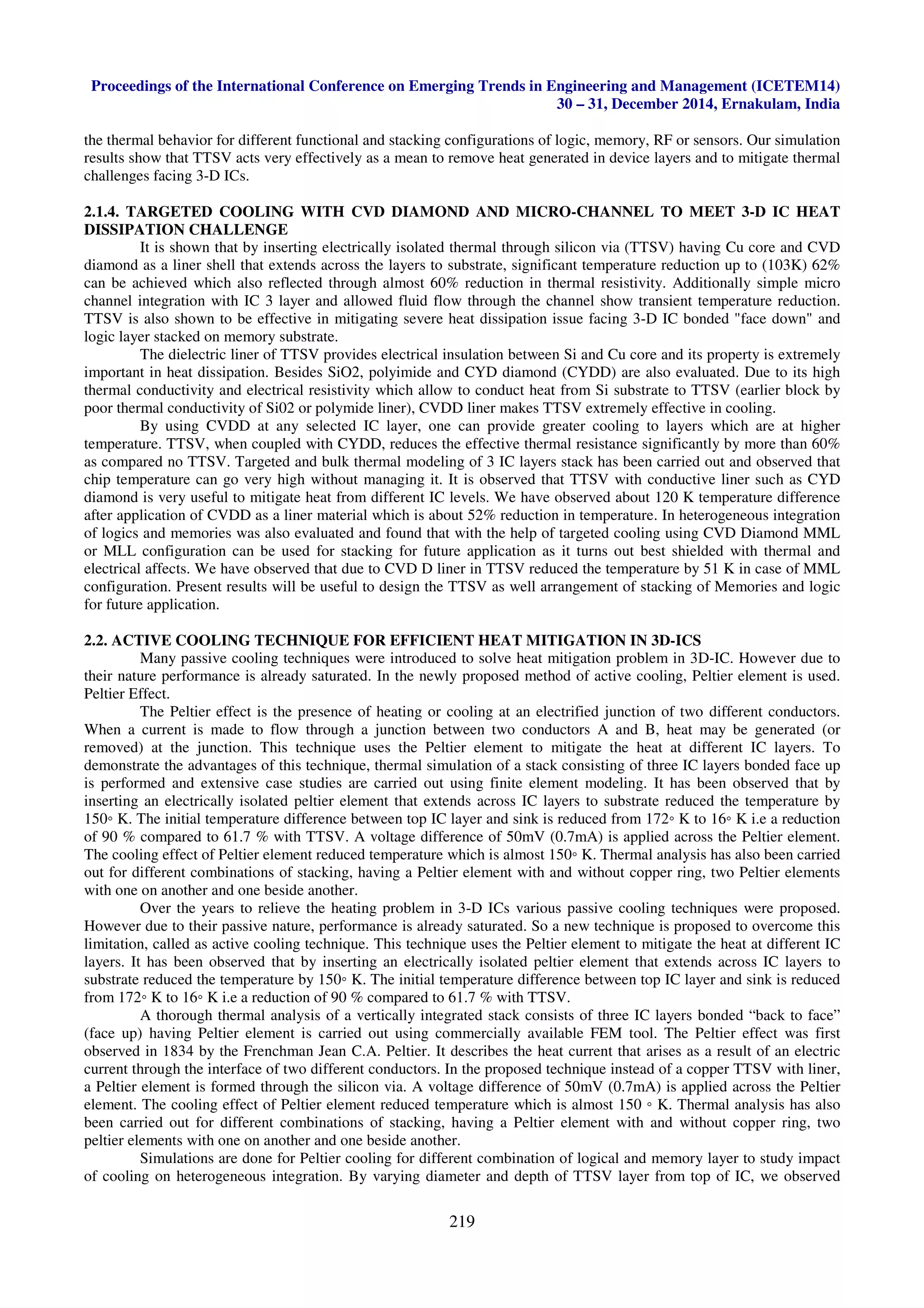
Fig 2: Th
2.1.3. IMPACT OF THERMAL THROUGH
TEMPERATURE PROFILE OF MUL
Shiv Govind Singh et al [6] presented IC performance is predominantly governed by
smaller wire cross-section, wire pitch and longer lines that t
capacitance hence signal latency of these lines. Material solutions
interconnects delay time as pitch is scaled down further. 3
to overcome this scaling barrier as it replaces long
interconnects. Thermal dissipation in present 2
device reliability in a negative manner. This problem is expected to be exacerbated further in 3
by every silicon layers must now be dissipated
the power density and is a potential show
Fig
The schematic of 3-D stack with TTSV is depicted in Figure 3. In this proposed model, heat is
device power and interconnects joule heating. The heat flux is generated by device is
and is in the range of 0.3 W/mm2 to 0.7 W/mm2. This power density
we also assume that interconnects joule heating is
interface between two chips.
This method also compared the temperature variation along the vertical distance from the top of
substrate) in Figure 3. TTSV reduces temperatures of all layers. Additionally, the impact
different IC layers has also been investigated. This allows one to
layer temperature. Another consideration is the
Figure 5, as the TTSV extends further into substrate, the temperature of IC1 at a point immediate to TTSV decreases
sharply and saturates when TTSV is about 10 m and further into substrate. On the other hand, IC1 temperature at a
distant point (>90 m) is not affected by the TTSV extension length. Thermal aware design is imperative
success and must be considered at early phase of design. The model presented in this work
International Conference on Emerging Trends in Engineering and Management (ICETEM14)
30 – 31, December 2014, Ernakulam, India
218
promising cooling technology solution to overcome the thermal challenges of 3D MPSoCs in HPC architectures. But
intelligent control of the coolant flow rate is needed to avoid wasted energy consumption for over
T IN 3D ICS.
Brent Goplen et al [4] proposed a method of incorporating thermal vias into integrated
promising way of mitigating thermal issues by lowering the thermal resistance of the chip itself. However, thermal vias
therefore, algorithms are needed to minimize their usage while placing them in areas
would make the greatest impact.
Thermal mesh or 3DIC, with thermal via regions
OUGH SILICON VIA (TTSV) ON THE
LTI-LAYER 3-D DEVICE STACK
Shiv Govind Singh et al [6] presented IC performance is predominantly governed by
section, wire pitch and longer lines that traverse across larger chips. These increase the resistance and
capacitance hence signal latency of these lines. Material solutions such as Cu/low-κ is no longer able to reduce
interconnects delay time as pitch is scaled down further. 3-D ICs with multiple active Si layers is a promising technique
to overcome this scaling barrier as it replaces long inter-block global wires with much shorter vertical inter
present 2-D circuits is known to significantly impact interconnect, performance and
a negative manner. This problem is expected to be exacerbated further in 3
every silicon layers must now be dissipated through a smaller 3-D chip foot print. This results in a sharp
the power density and is a potential show-stopper to 3-D ICs if left unmanaged
ig 3: The schematic of 3-D stack with TTSV
D stack with TTSV is depicted in Figure 3. In this proposed model, heat is
device power and interconnects joule heating. The heat flux is generated by device is homogeneous across the entire chip
and is in the range of 0.3 W/mm2 to 0.7 W/mm2. This power density is applied at the top of each Si layers. In addition
we also assume that interconnects joule heating is homogeneous across the entire chip and is applied at the bonding
This method also compared the temperature variation along the vertical distance from the top of
substrate) in Figure 3. TTSV reduces temperatures of all layers. Additionally, the impact of various TTSV diameters on
different IC layers has also been investigated. This allows one to determine the required TTSV diameter given a desire
layer temperature. Another consideration is the impact of TTSV extension length into silicon substrate. As can be seen in
further into substrate, the temperature of IC1 at a point immediate to TTSV decreases
saturates when TTSV is about 10 m and further into substrate. On the other hand, IC1 temperature at a
distant point (>90 m) is not affected by the TTSV extension length. Thermal aware design is imperative
success and must be considered at early phase of design. The model presented in this work can be applied to understand
Engineering and Management (ICETEM14)
31, December 2014, Ernakulam, India
MPSoCs in HPC architectures. But
wasted energy consumption for over-cooling the system
corporating thermal vias into integrated circuits (ICs) is a
resistance of the chip itself. However, thermal vias
to minimize their usage while placing them in areas
Shiv Govind Singh et al [6] presented IC performance is predominantly governed by interconnects delay due to
chips. These increase the resistance and
κ is no longer able to reduce
tiple active Si layers is a promising technique
block global wires with much shorter vertical inter-layer
D circuits is known to significantly impact interconnect, performance and
a negative manner. This problem is expected to be exacerbated further in 3-D ICs as power generated
D chip foot print. This results in a sharp increase in
D stack with TTSV is depicted in Figure 3. In this proposed model, heat is generated due to
homogeneous across the entire chip
is applied at the top of each Si layers. In addition,
homogeneous across the entire chip and is applied at the bonding
This method also compared the temperature variation along the vertical distance from the top of IC1 layer (i.e.
of various TTSV diameters on
determine the required TTSV diameter given a desired
impact of TTSV extension length into silicon substrate. As can be seen in
further into substrate, the temperature of IC1 at a point immediate to TTSV decreases
saturates when TTSV is about 10 m and further into substrate. On the other hand, IC1 temperature at a
distant point (>90 m) is not affected by the TTSV extension length. Thermal aware design is imperative for 3-D ICs
can be applied to understand](https://image.slidesharecdn.com/activecoolingtechniqueusingpeltierelementforefficientheatmitigationin3dicsacomparativestudy-141216082142-conversion-gate01/75/Active-cooling-technique-using-peltier-element-for-efficient-heat-mitigation-in-3-dics-a-comparative-study-3-2048.jpg)
![Proceedings of the International Conference on Emerging Trends in Engineering and Management (ICETEM14)
30 – 31, December 2014, Ernakulam, India
220
better cooling is achieved by increasing diameter of Peltier element and no significant variation with depth. Better heat
reduction is seen for multiple Peltier elements than single peltier element of same area. It also provides approximately
lesser variation in temperature profile across the top IC layer. It is shown that for heterogeneous integration irrespective
of their stacking combination, temperature can be reduced at any IC layer.
3. COMPARATIVE ANALYSIS
Different methods of cooling in IC technology, both active and passive methods are compared.
Table 1: Comparative analysis of cooling techniques in IC
4. CONCLUSION
Management of thermal issues is central to the development of future generation microprocessors, integrated
networks, and other highly integrated systems. It is rapidly becoming one of the most challenging issues in high-
performance chip design due to ever increasing device count and clock speed. Thermal problems have important
implications for performance and reliability. Different cooling techniques are introduced to eliminate heat problem in
3D-IC. Passive methods are less used because their performance is already saturated.
REFERENCES
[1] Sungjun Im and Kaustav Banerjee Center for Integrated Systems, Stanford University, Stanford, CA 94305.
[2] A. Rahman, R. Reif, “Thermal analysis of three-dimensional (3-D) integrated circuits (ICs)” in Proc. IITC,
pp. 157159, 2001.
[3] Mohamed M. Sabry, “Towards Thermally-Aware Design of 3D MPSoCs with Inter-Tier Cooling”.
[4] Brent Goplen, “Thermal Via Placement in 3D ICs”.
[5] A. A. Khan, S. B. Patel, D. Chaturvedi, A. Dutta, S. G. Singh, “Targeted cooling with CVD diamond and micro-
channel to meet 3-D IC heat dissipation challenge,” IEEE ICEE , Dec. 2012.
[6] Aftab Alam Khan, Shabaz Basheer Patel, Divanshu Chaturvedi, Ashudeb Dutta, Shivgovind Singh Electrical
Engineering Department, IIT-Hyderabad, Hyderabad, India [7]Lee et al, “full Chip Thermal analysis of Planner
and vertically integrated High performance ICs, 2000.
[7] S. Singh, C. S. Tan, “Thermal mitigation using thermal through silicon via (TTSV) in 3-D IC”, IEEE IMPACT
conference Taiwan, pp. 182–184, 2009.
[8] S. Lee, T.F. Lemczyk, and M. M. Yovanovich, “Analysis of Thermal Vias in High Density Interconnect
Technology,” in 8th IEEE Semi-Therm Symposium, pp. 55-61, Feb. 1992.
[9] R.S. Li, “Optimization of Thermal Via Design Parameters Based on an Analytical Thermal Resistance Model,”
in Thermal and Thermomechanical Phenomena in Electronic Systems, pp. 475-480, 1998.
[10] D. Pinjala, M.K. Iyer, Chow Seng Guan, and I.J. Rasiah, “Thermal characterization of vias using compact
models,” in Proc. of the Electronics Packaging Technology Conf., pp. 144-147, Dec. 2000.
[11] T-Y Chiang, K. Banerjee, and K. C. Saraswat, “Effect of Via Separation and Low-k Dielectric Materials on the
Thermal Characteristics of Cu Interconnects,” in IEEE Int. Electron Devices Meeting Tech. Digest, pp. 261-264,
2000.
[12] T-Y. Chiang, K. Banerjee, and K. C. Saraswat, "Compact Modeling and SPICE-Based Simulation for
Electrothermal Analysis of Multilevel ULSI Interconnects," in Proc. of the Int. Conf. on Comput.-Aided Des.,
pp. 165-172, Nov. 2001.
Author Year Method Advantage Disadvantage
Lee et al 2000 Thermal via island. Simple process. Use of Si area which can be
used for new functionality.
Rahman et al. 2001 Thermal via made of Cu. More heat reduction. Use of Si area which can be
used for new functionality
Singh et al 2009 TTSV. Significant reduction
of top level heat.
Technique is passive in nature
Aftab et al 2012 Use of Conductive CVD
diamond as a liner.
Further heat reduction
of∼103 ◦K.
Technique is passive in nature
Pramod et alJ 2014 Active cooling technique
with the use of Peltier
element
Further heat reduction
of∼150 ◦K.
Active method of cooling.
Performance is not saturated.](https://image.slidesharecdn.com/activecoolingtechniqueusingpeltierelementforefficientheatmitigationin3dicsacomparativestudy-141216082142-conversion-gate01/75/Active-cooling-technique-using-peltier-element-for-efficient-heat-mitigation-in-3-dics-a-comparative-study-5-2048.jpg)

The document discusses the challenges and methods of heat mitigation in three-dimensional integrated circuits (3D ICs), highlighting the advantages of 3D architecture over traditional 2D circuits. It presents a comparative study of various active and passive cooling techniques, specifically focusing on the use of Peltier elements and innovative cooling methodologies like micro-channel liquid cooling. Effective thermal management is deemed crucial for enhancing performance and reliability as device density and clock speeds increase in modern chip designs.


![Coded Agents – with UiPath SDK + LangGraph [Virtual Hands-on Workshop]](https://cdn.slidesharecdn.com/ss_thumbnails/codedagentsdeck-251215155422-5497c599-thumbnail.jpg?width=640&height=640&fit=bounds)


