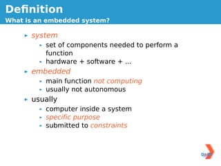
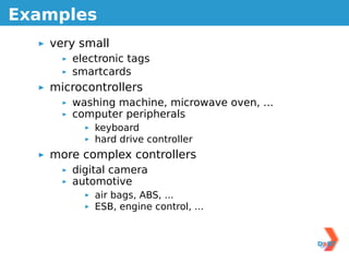
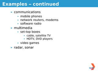
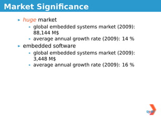
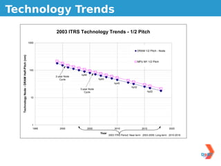
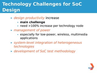
The document discusses challenges in system-on-chip design. The main challenges are:
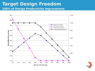
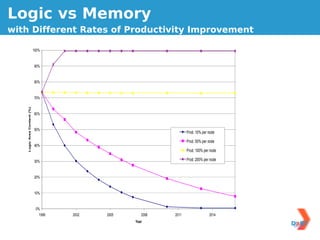
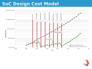
1. Increasing design productivity by over 100% per technology node to keep up with Moore's Law scaling.
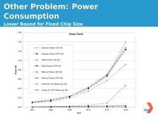
2. Managing power, especially for low-power, wireless, and multimedia applications.
3. Integrating heterogeneous technologies like MEMS and optoelectronics at the system level.
4. Developing test methodologies for system-on-chips, including reusable tests and built-in self-test for analog and digital components.


![[Duality Inc.] Double Sided Padless Sensor Chip](https://cdn.slidesharecdn.com/ss_thumbnails/visuals16-150227081719-conversion-gate02-thumbnail.jpg?width=640&height=640&fit=bounds)