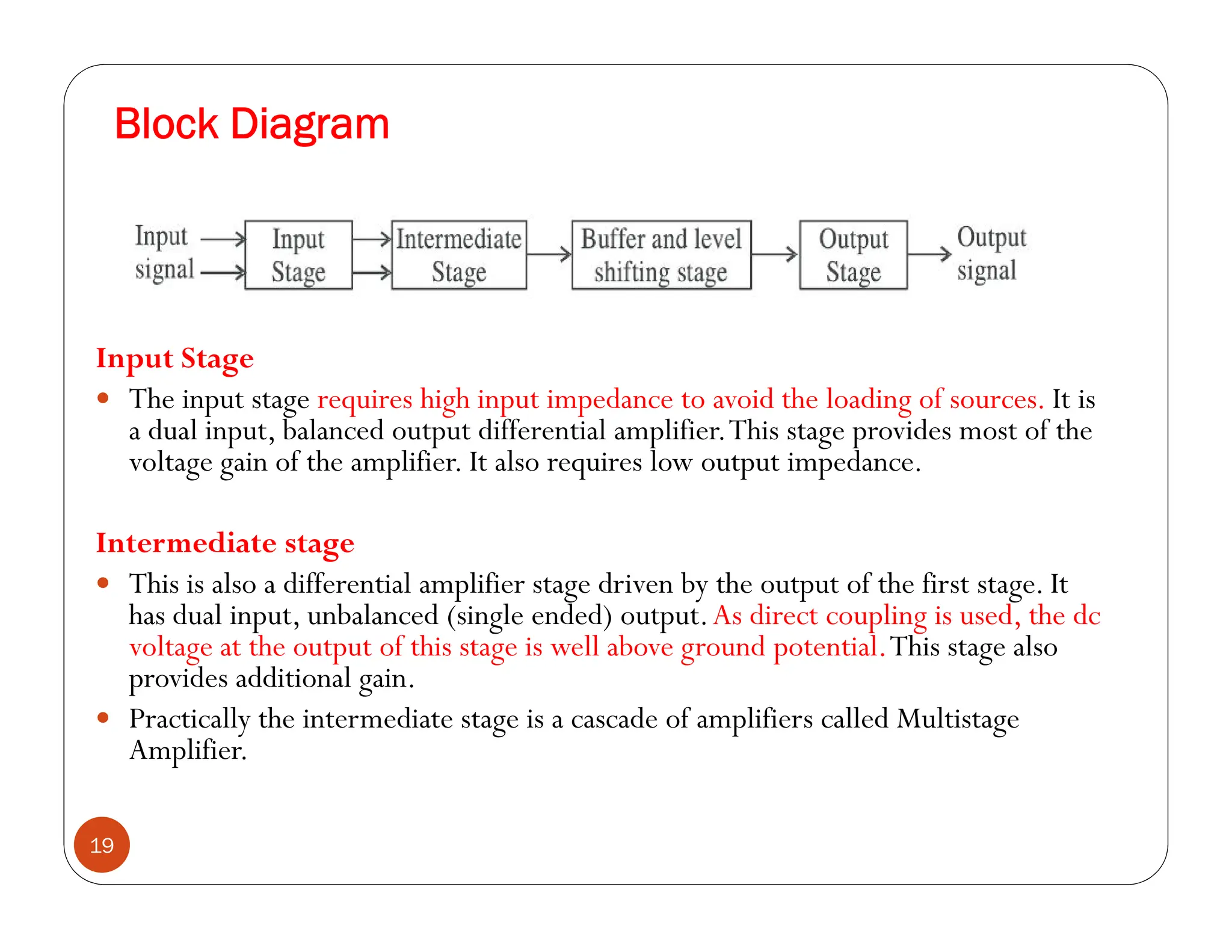
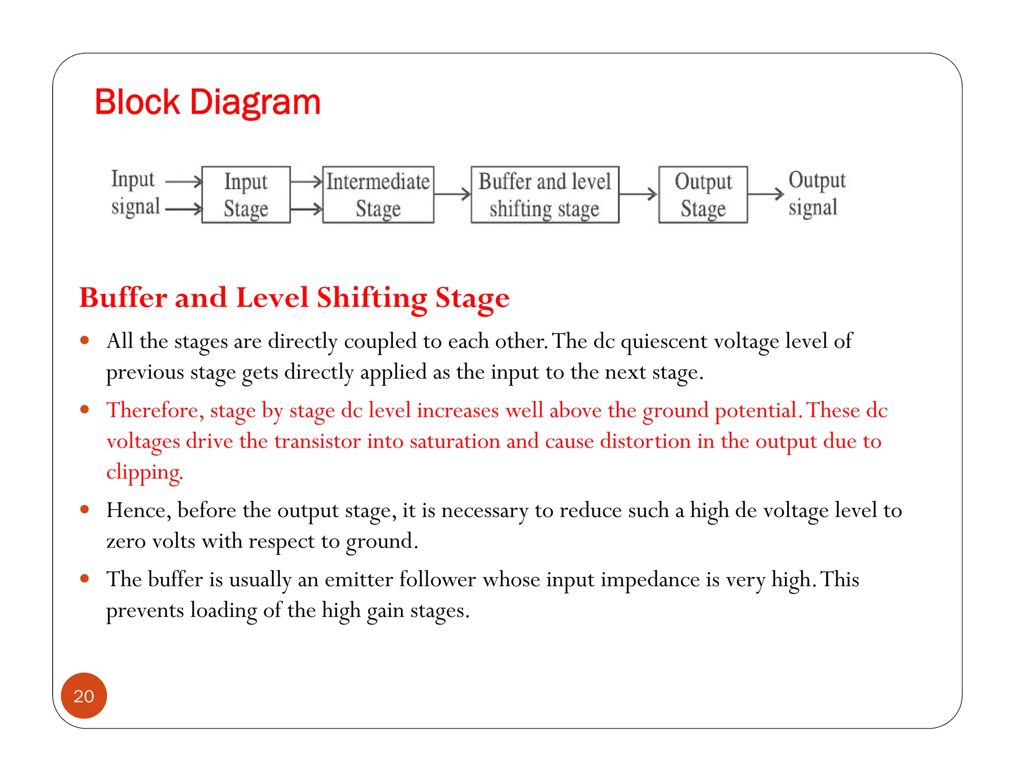
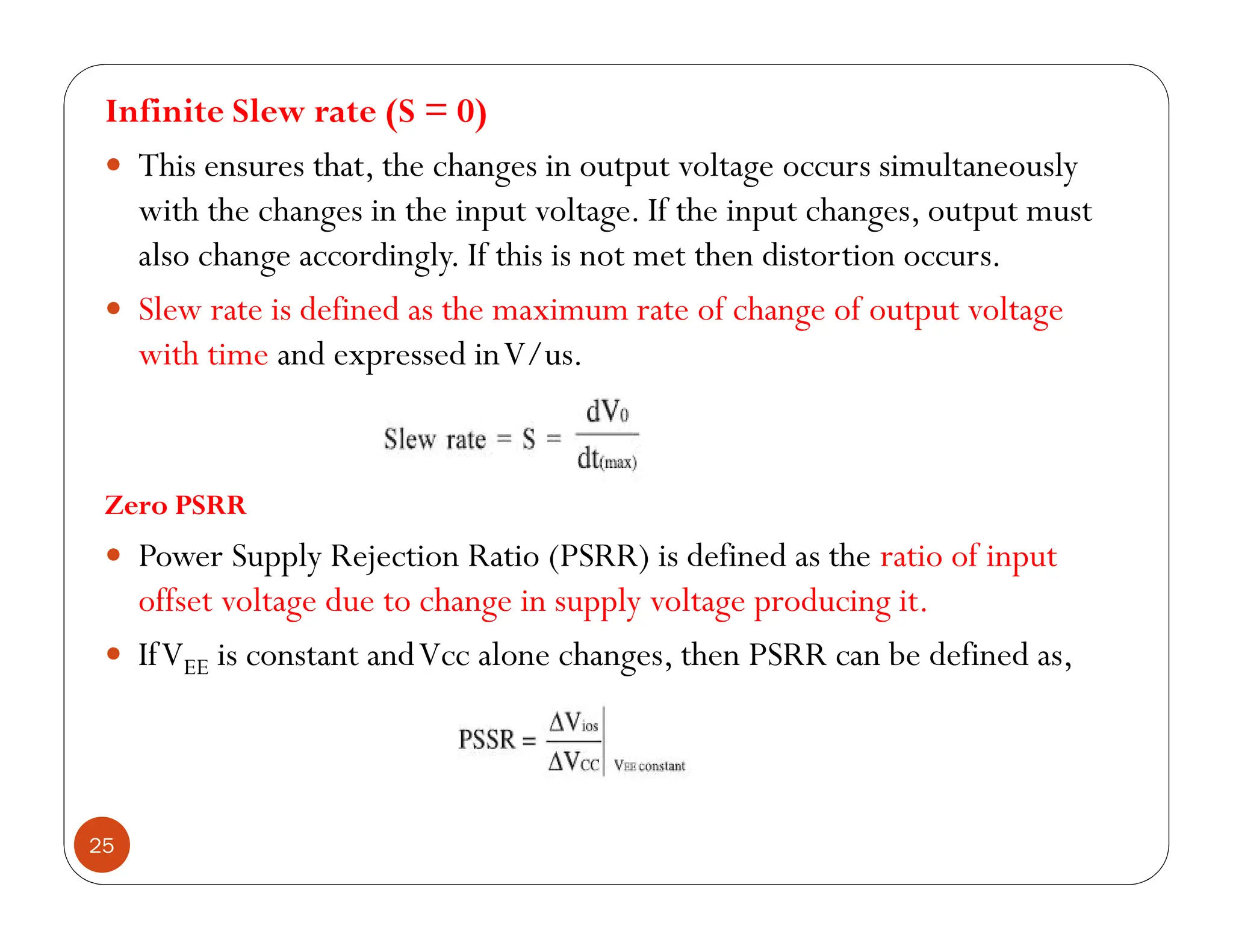
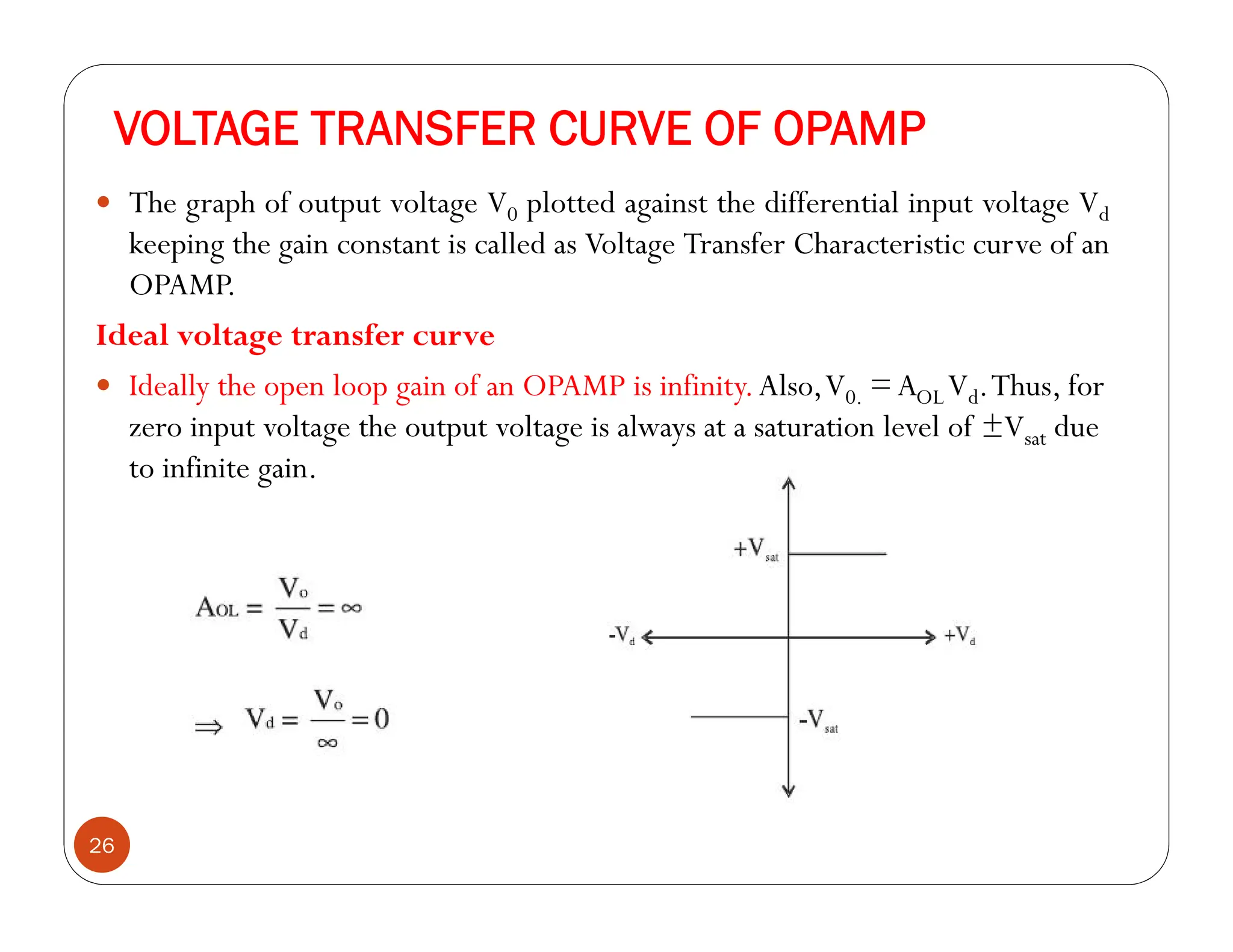
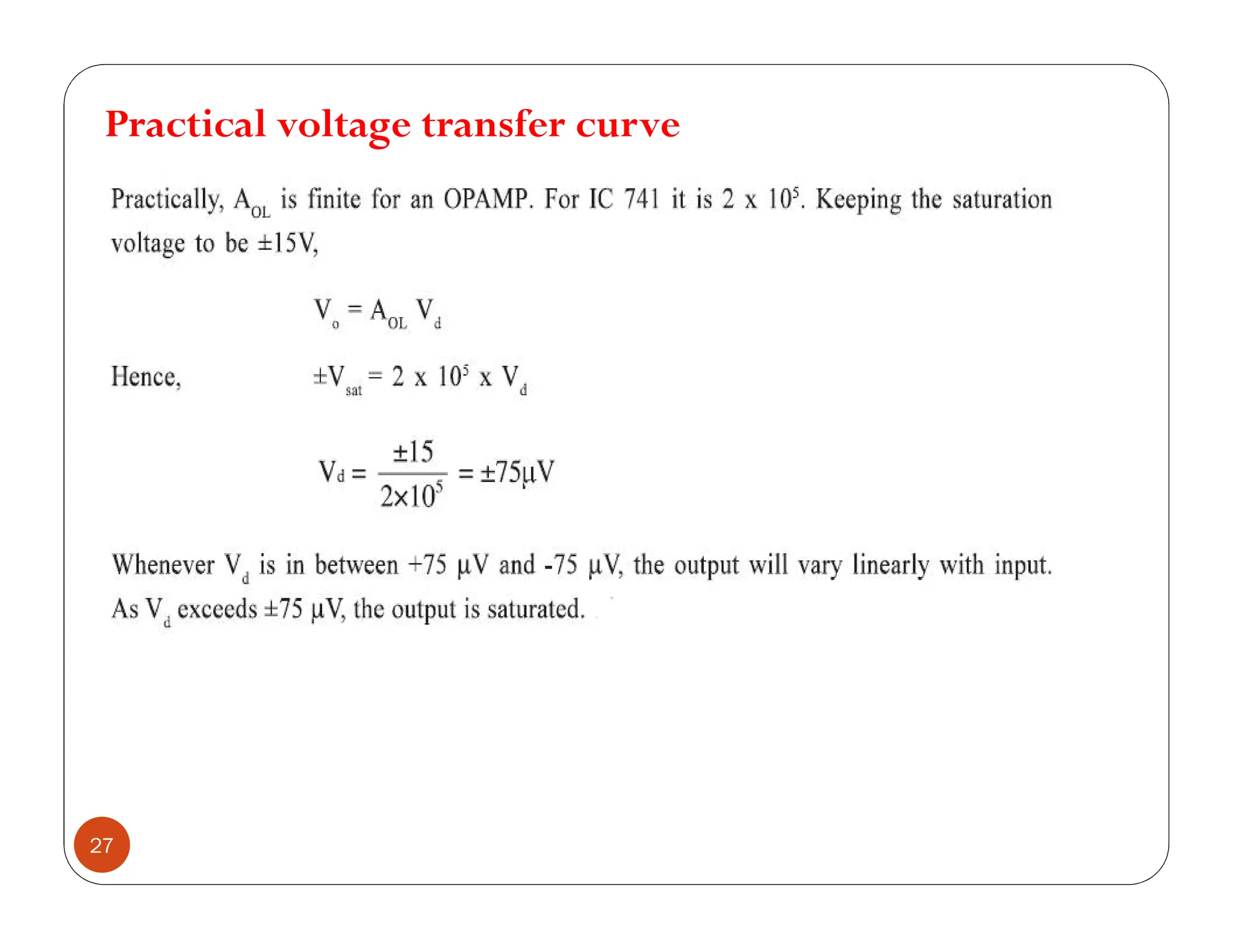
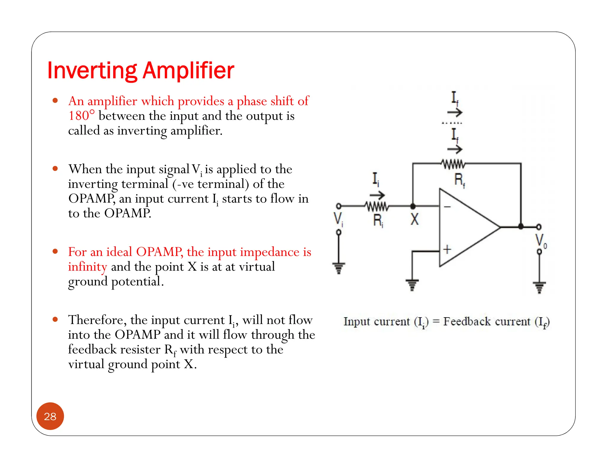
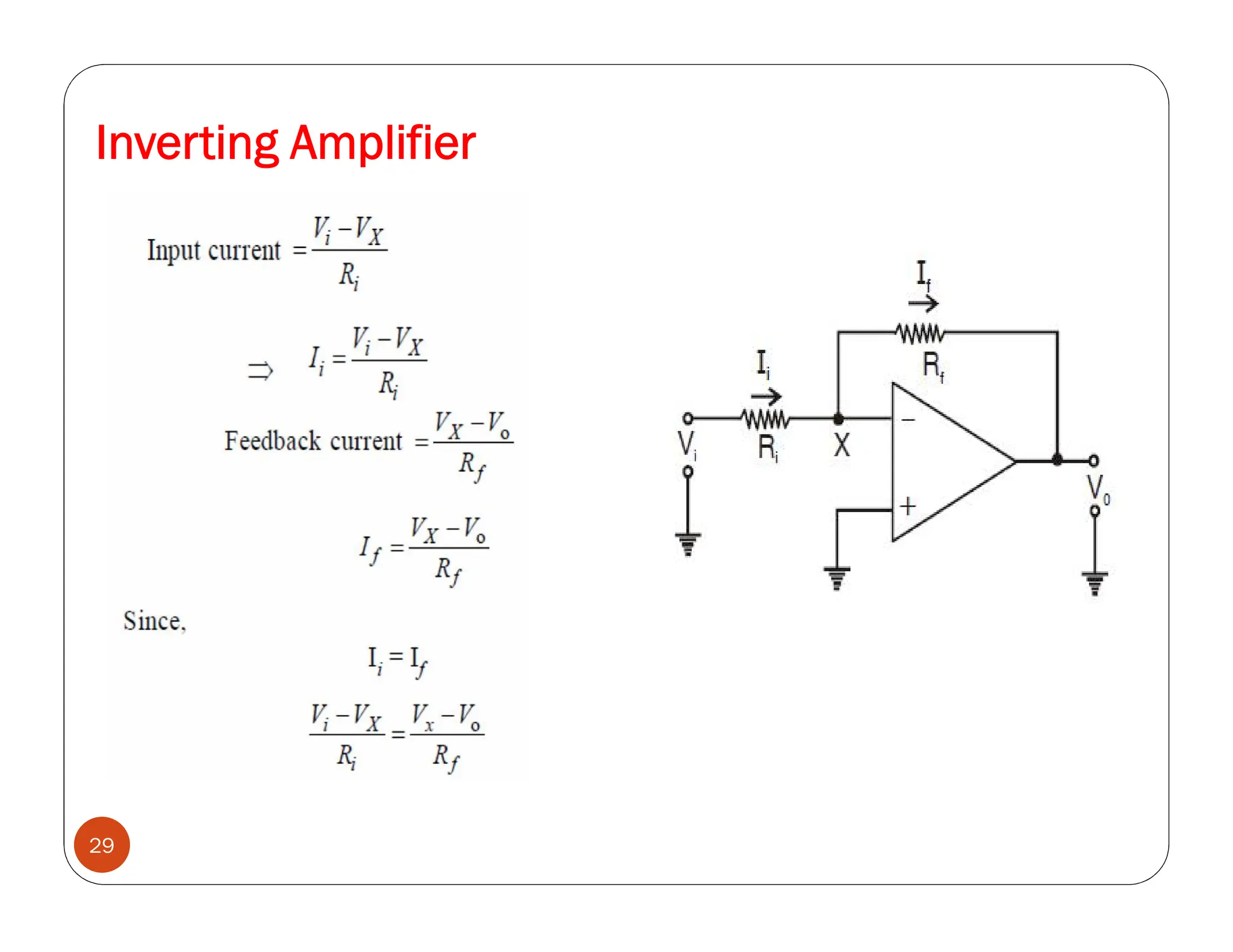
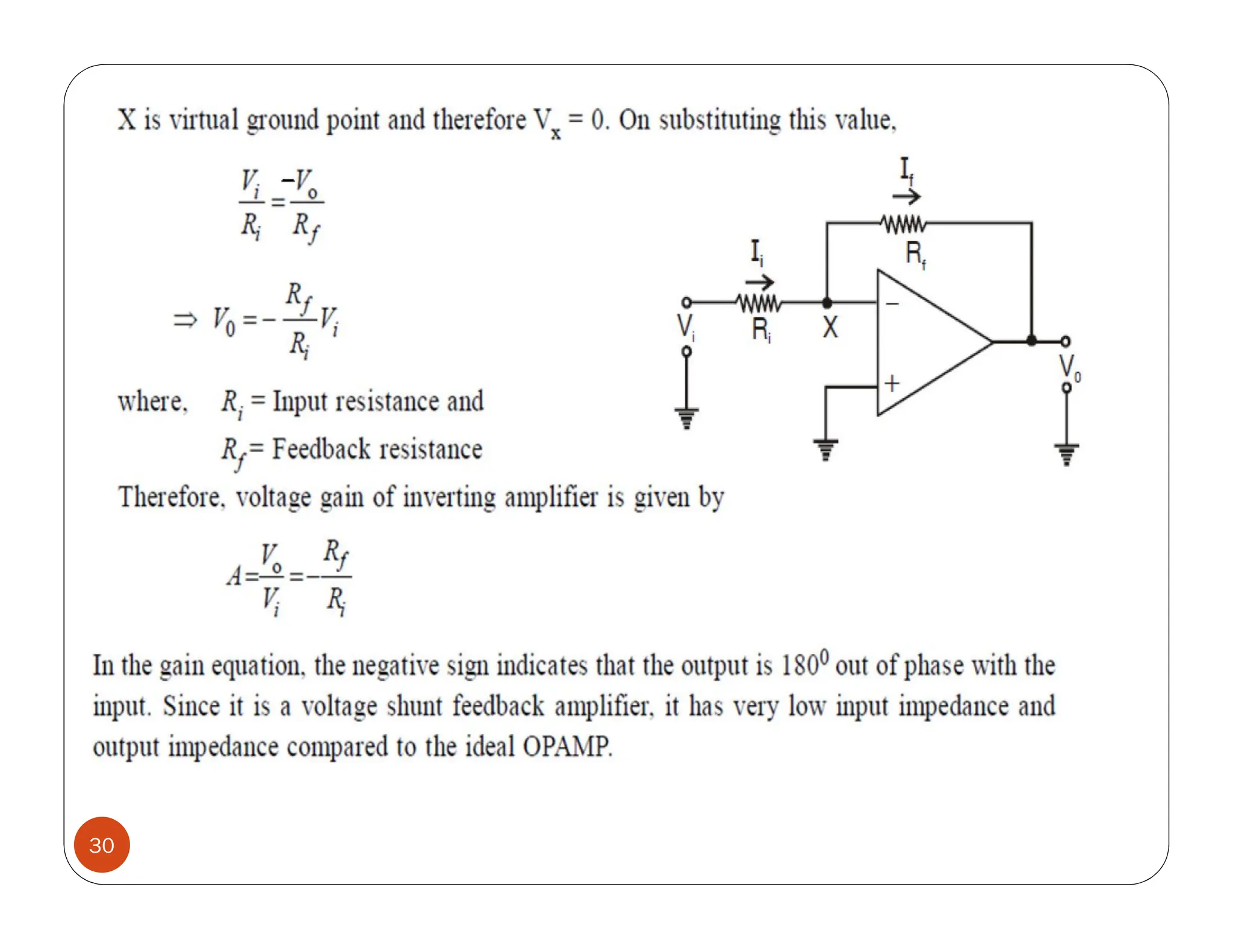
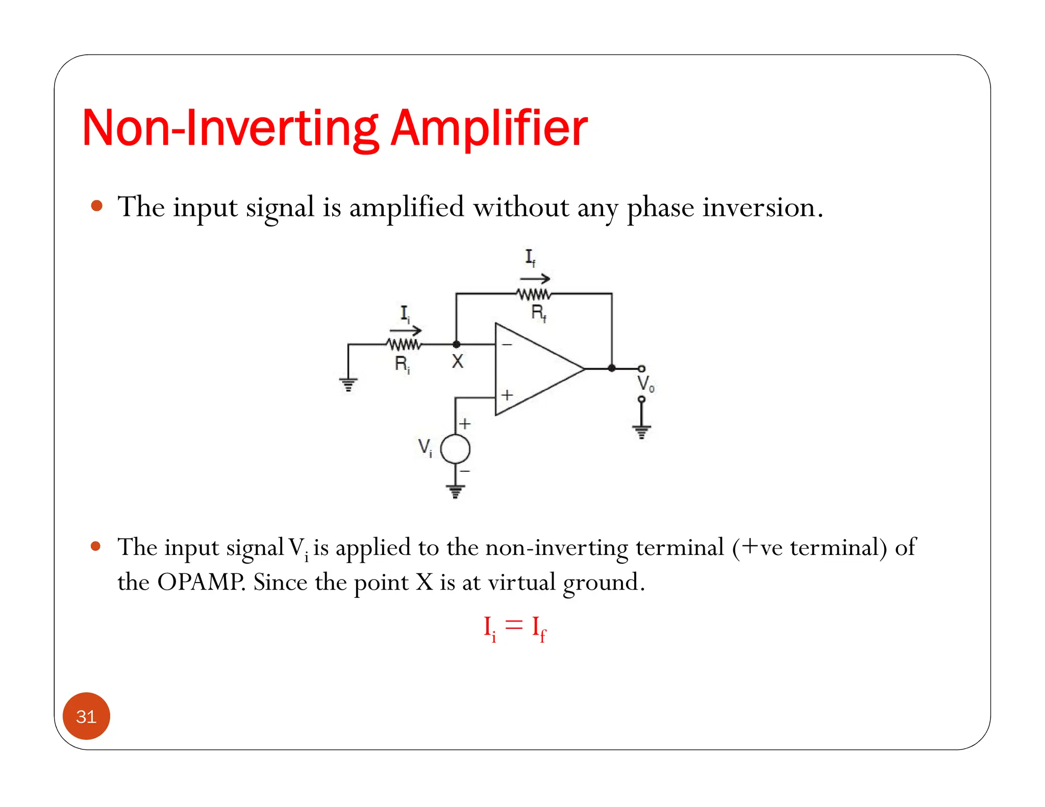
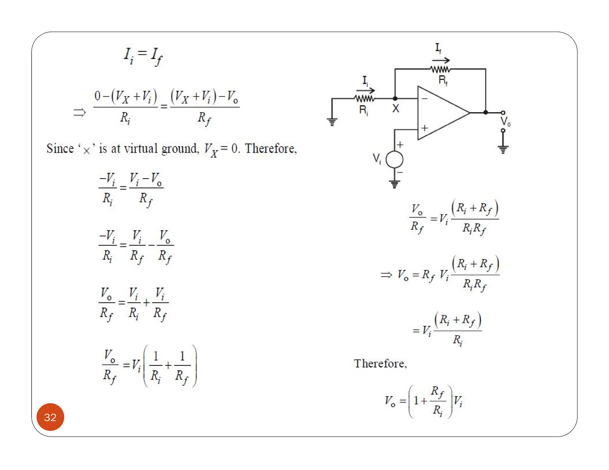
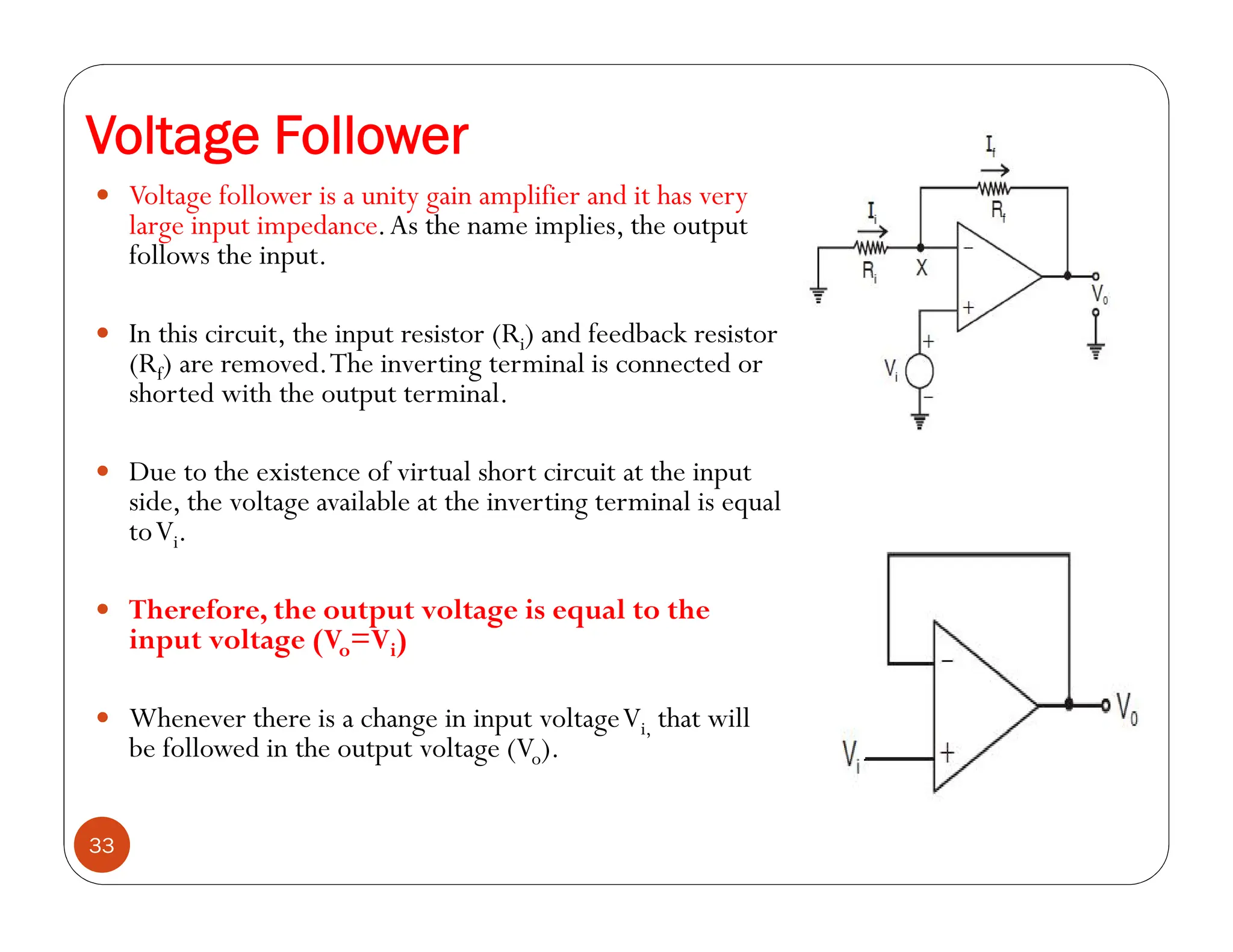
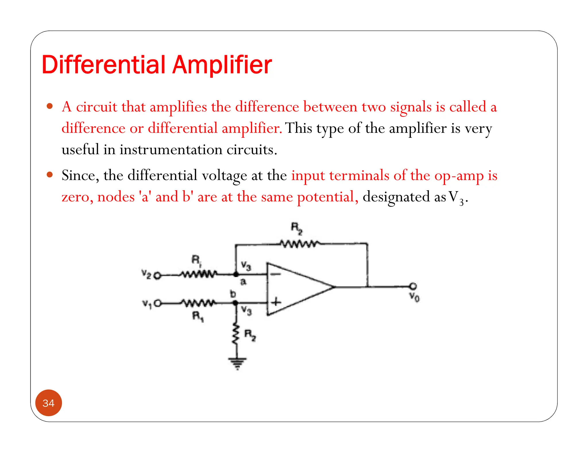
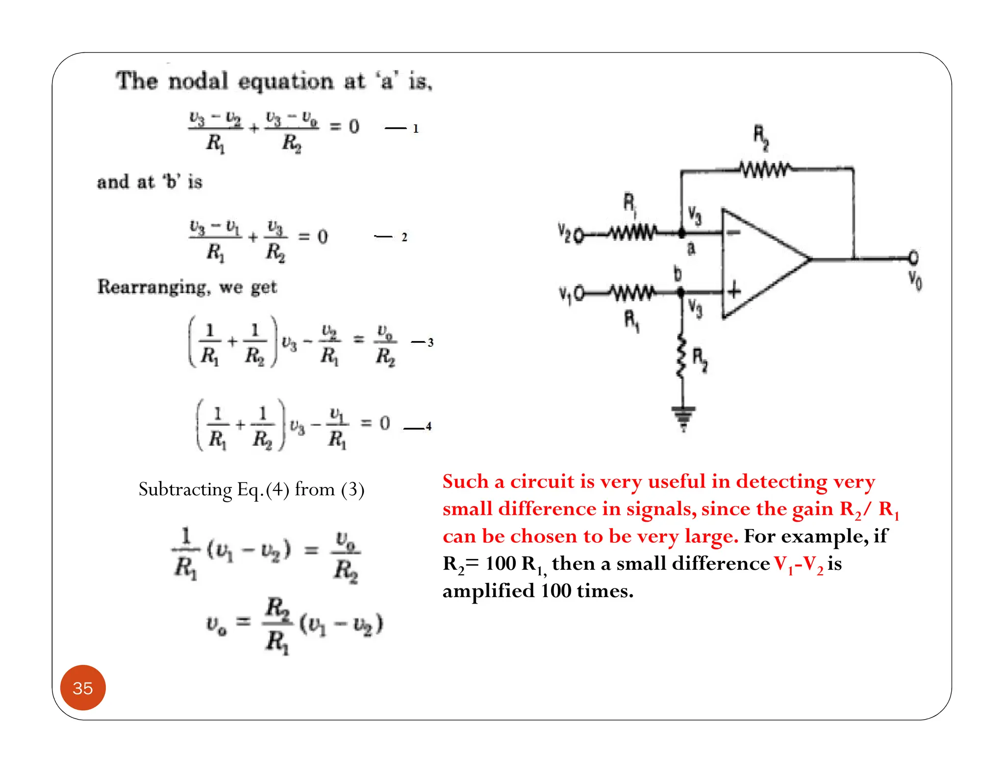
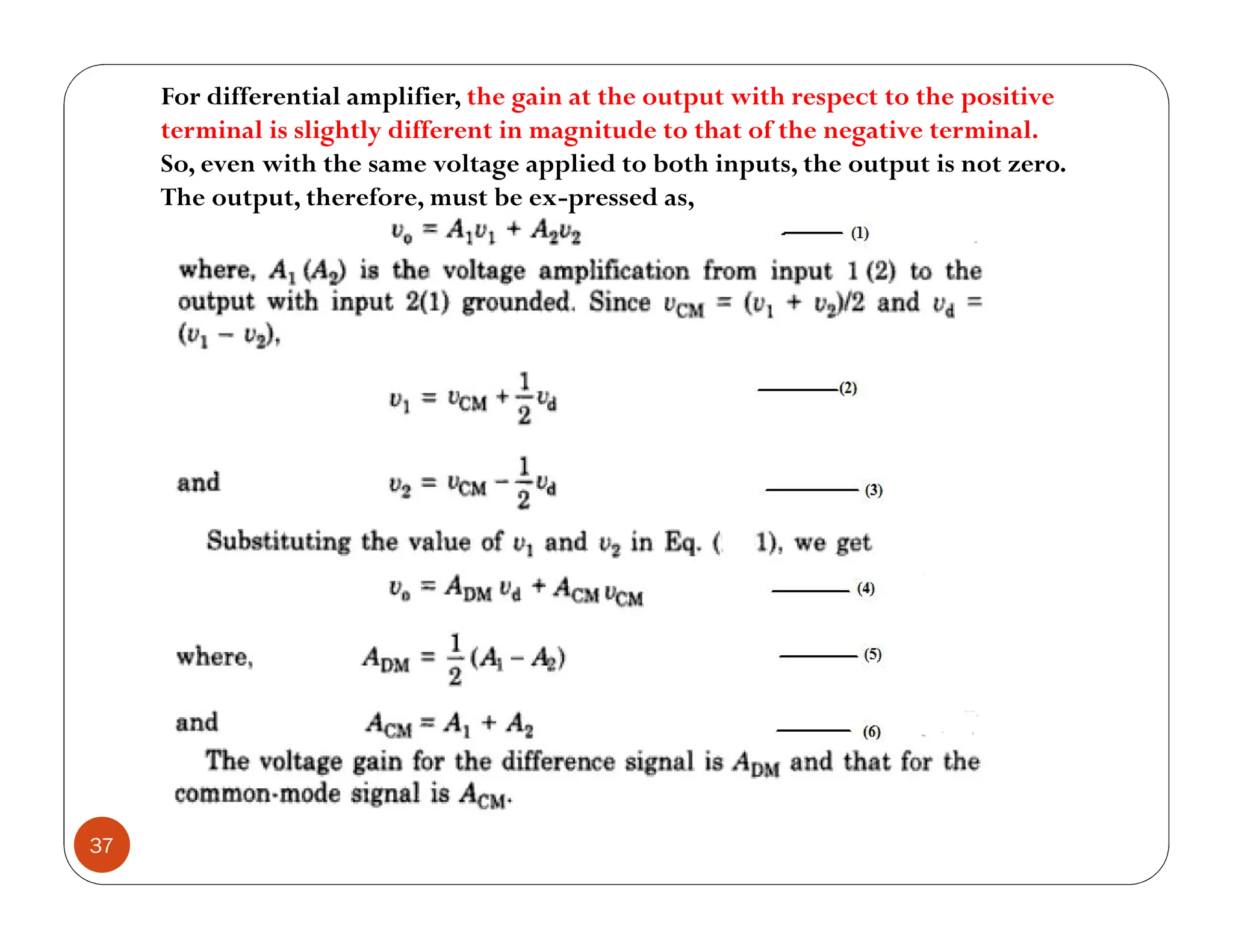
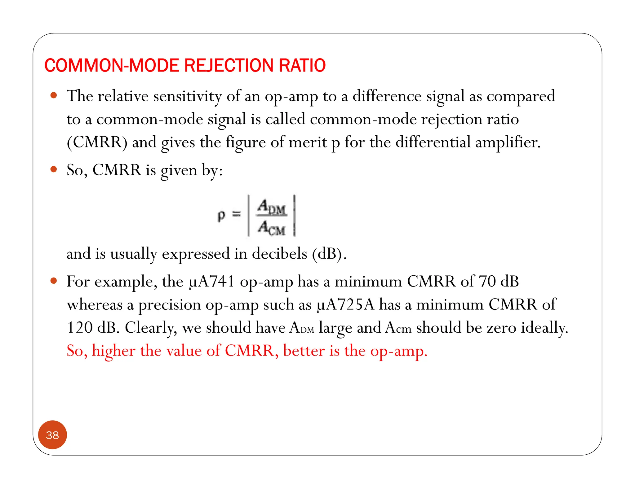
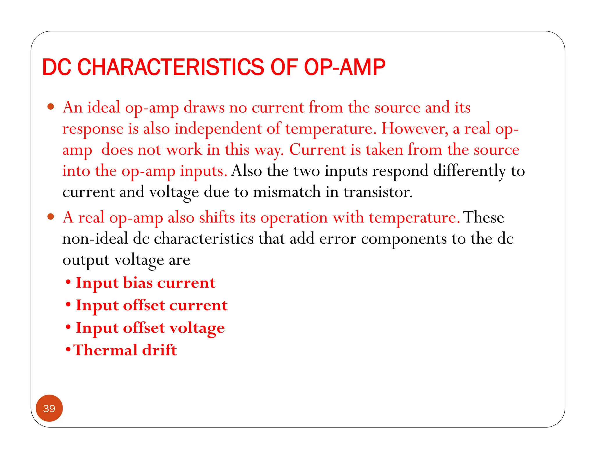
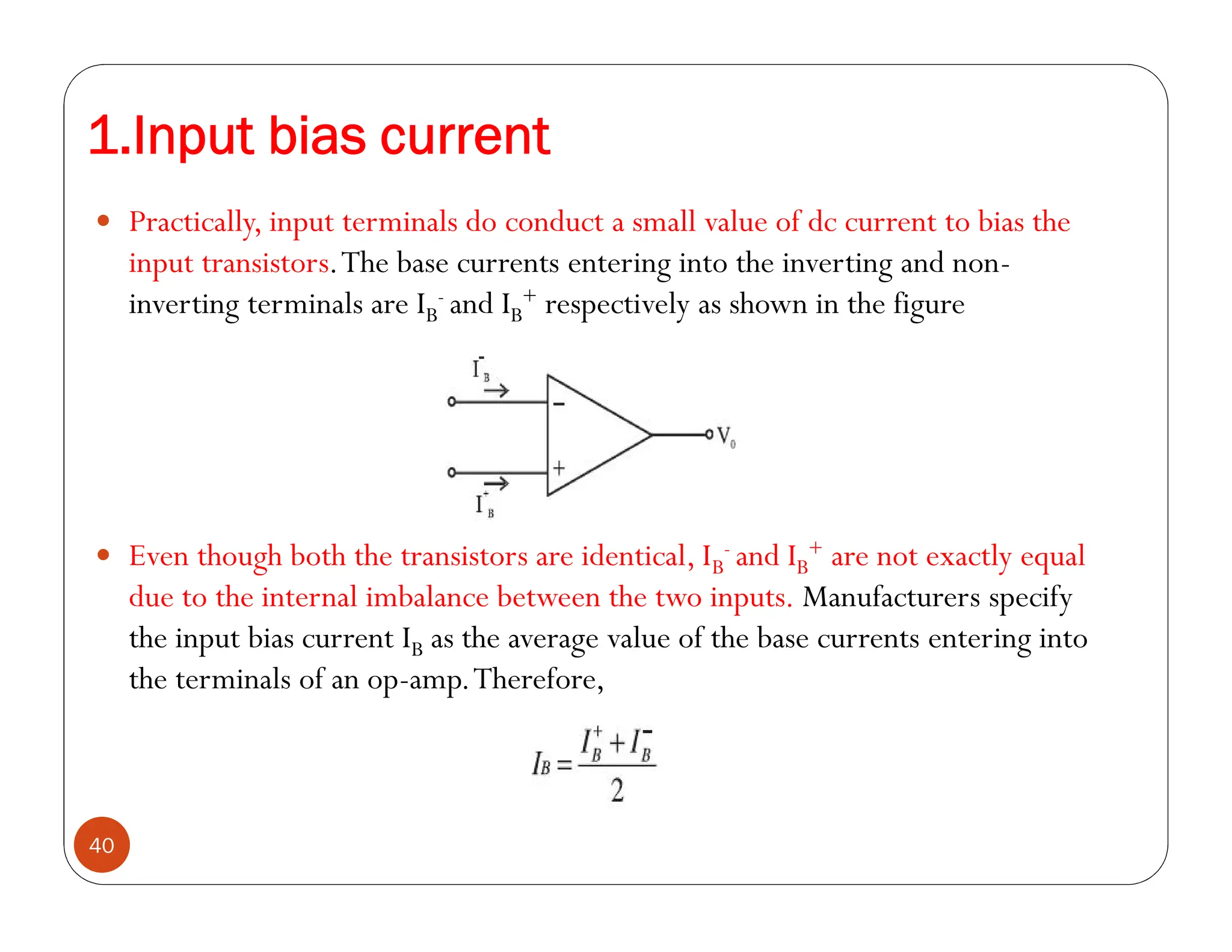
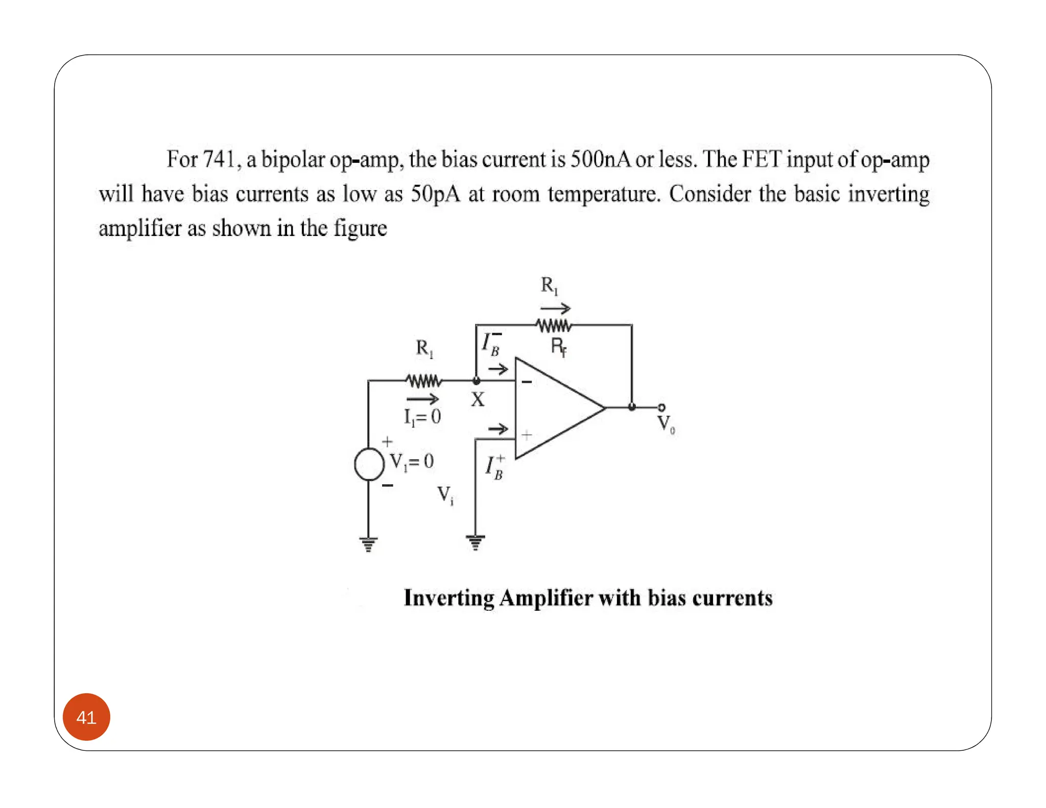
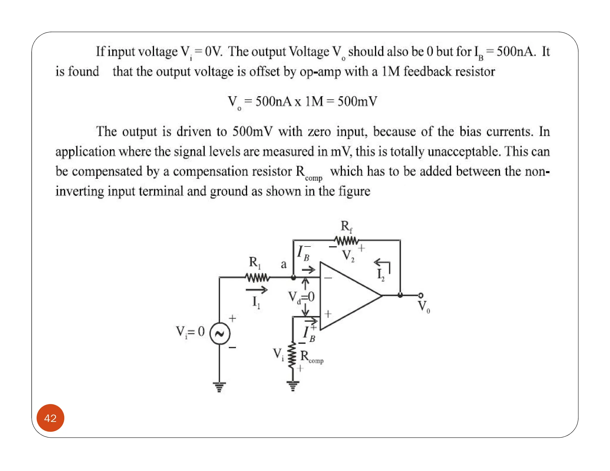
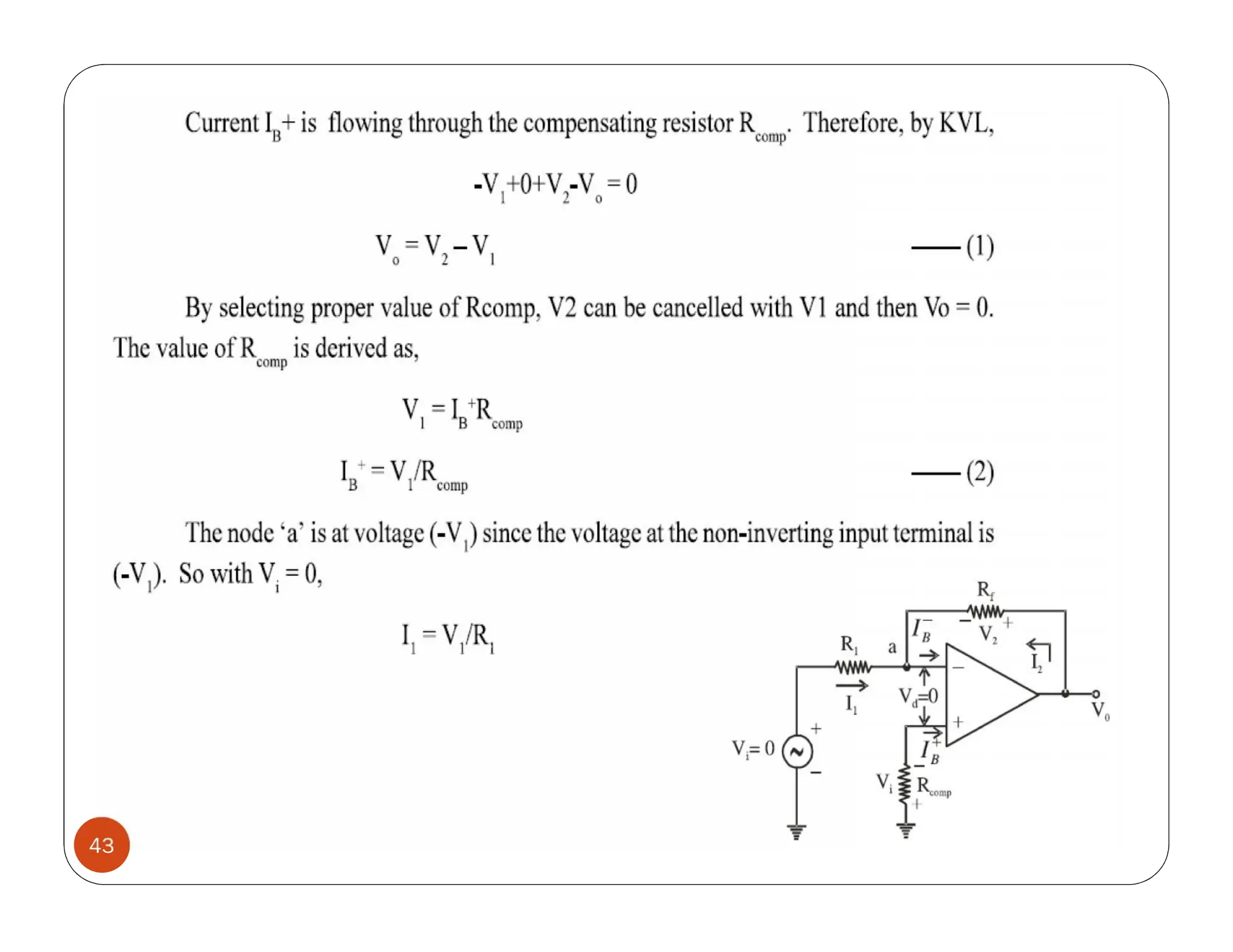
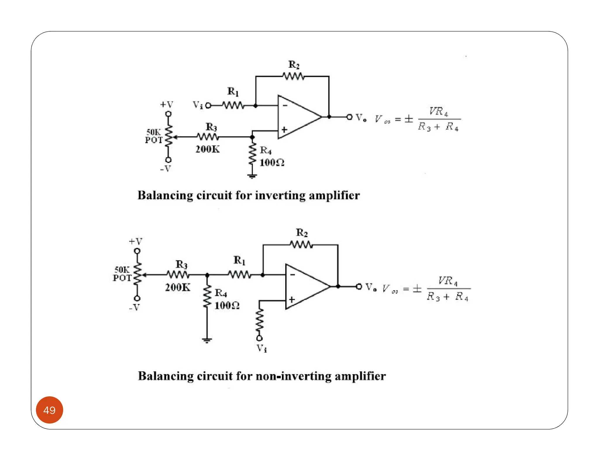
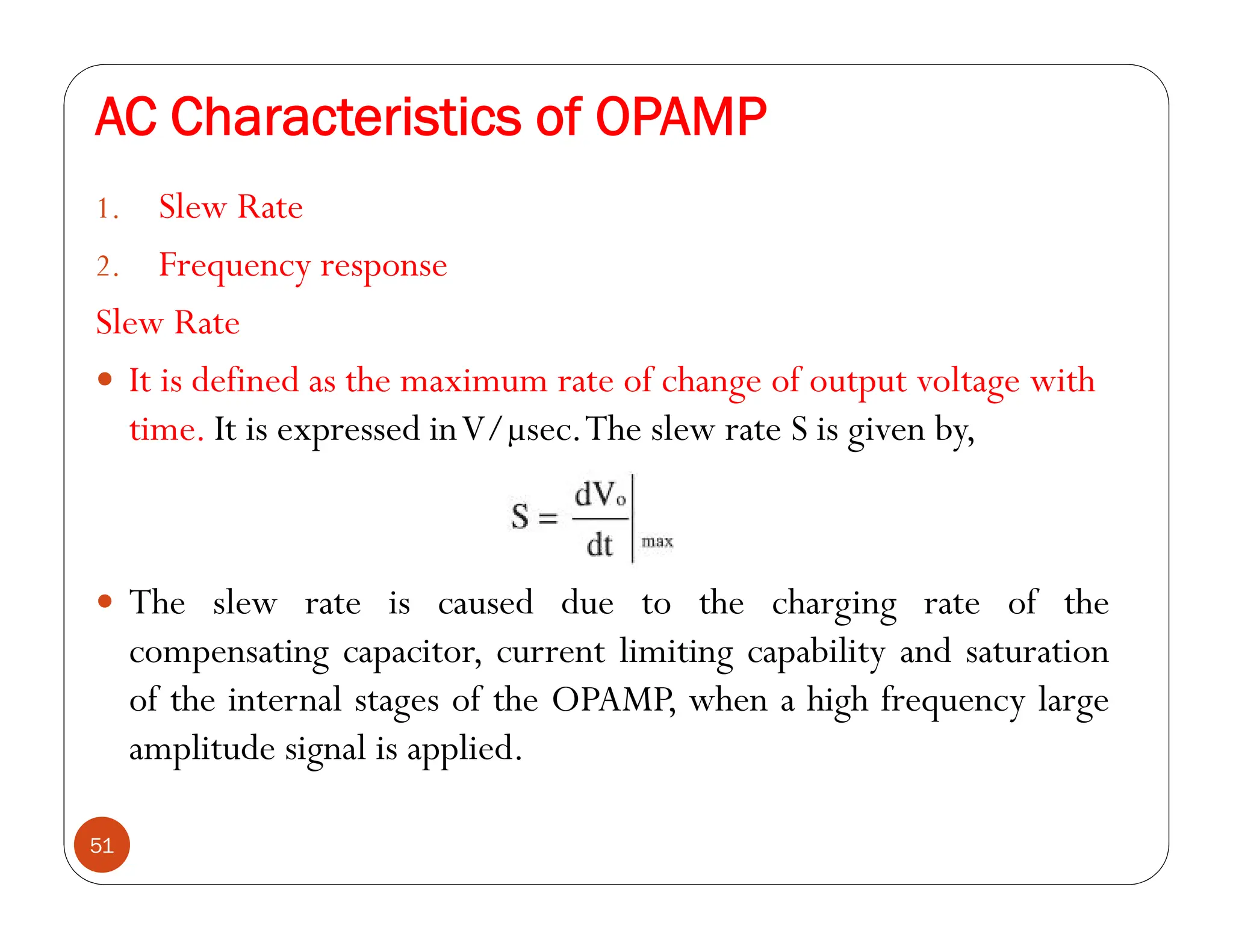
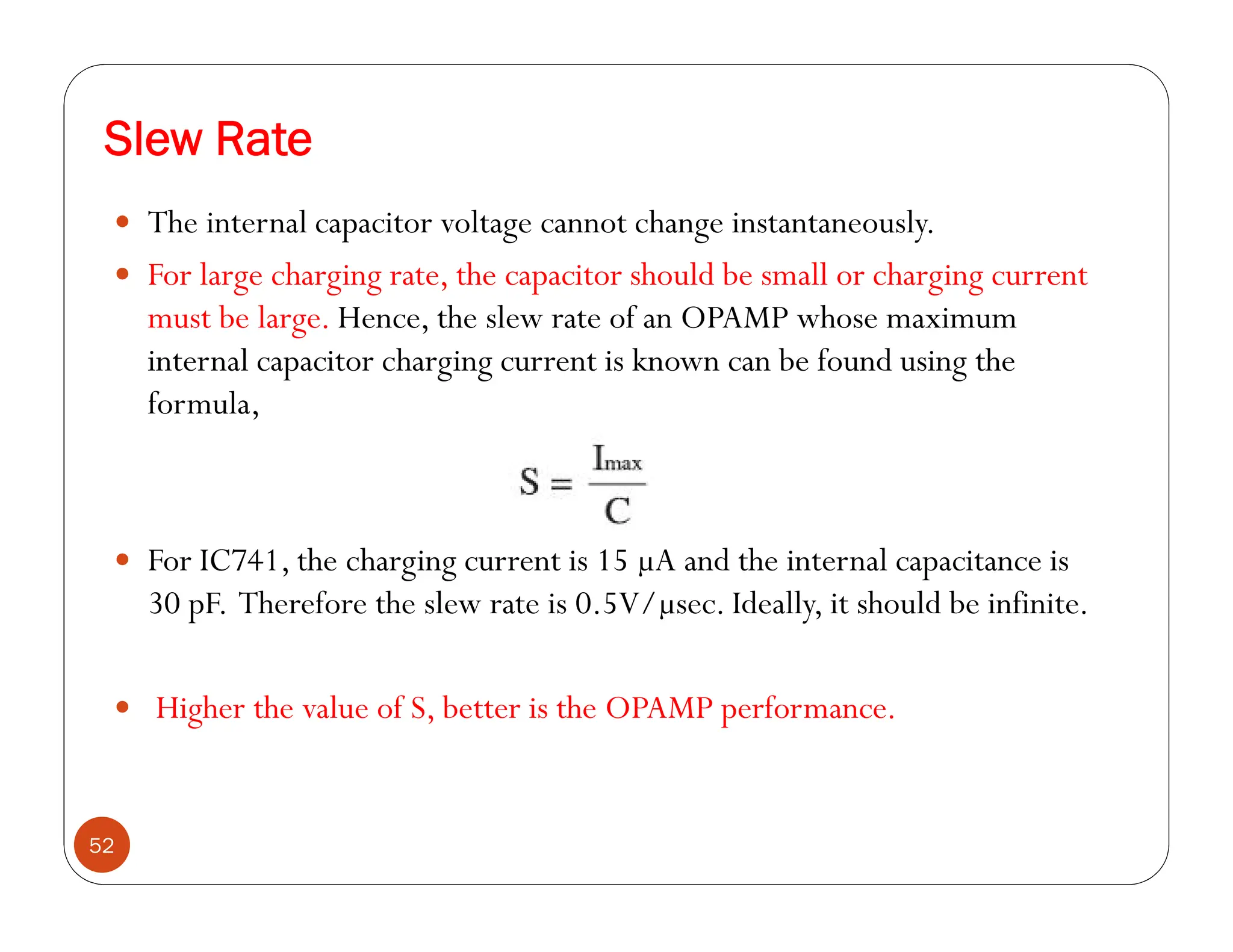
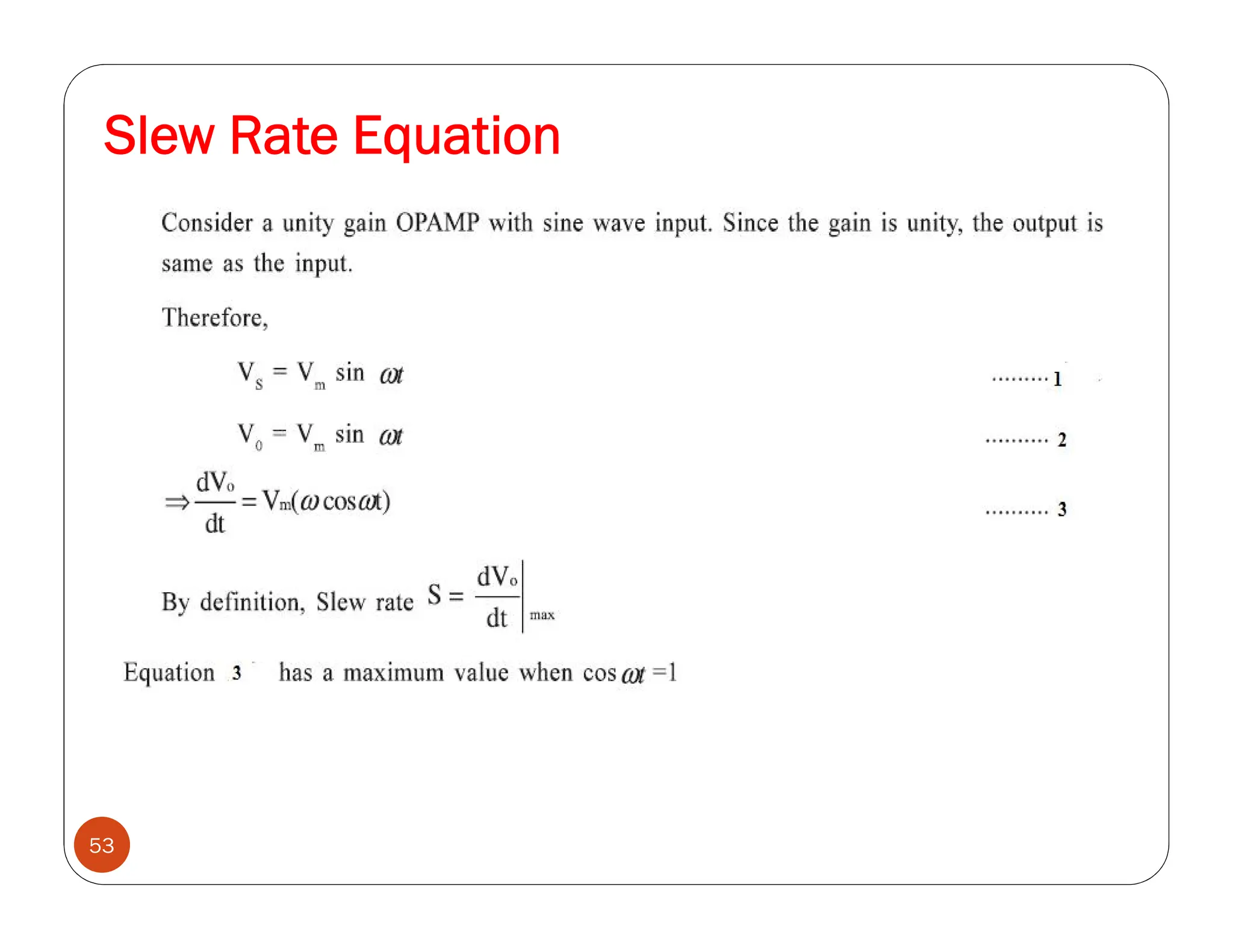
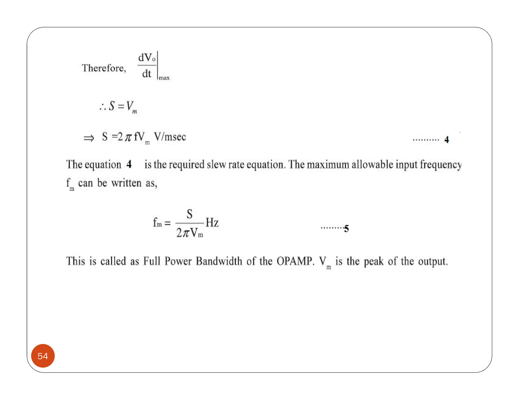
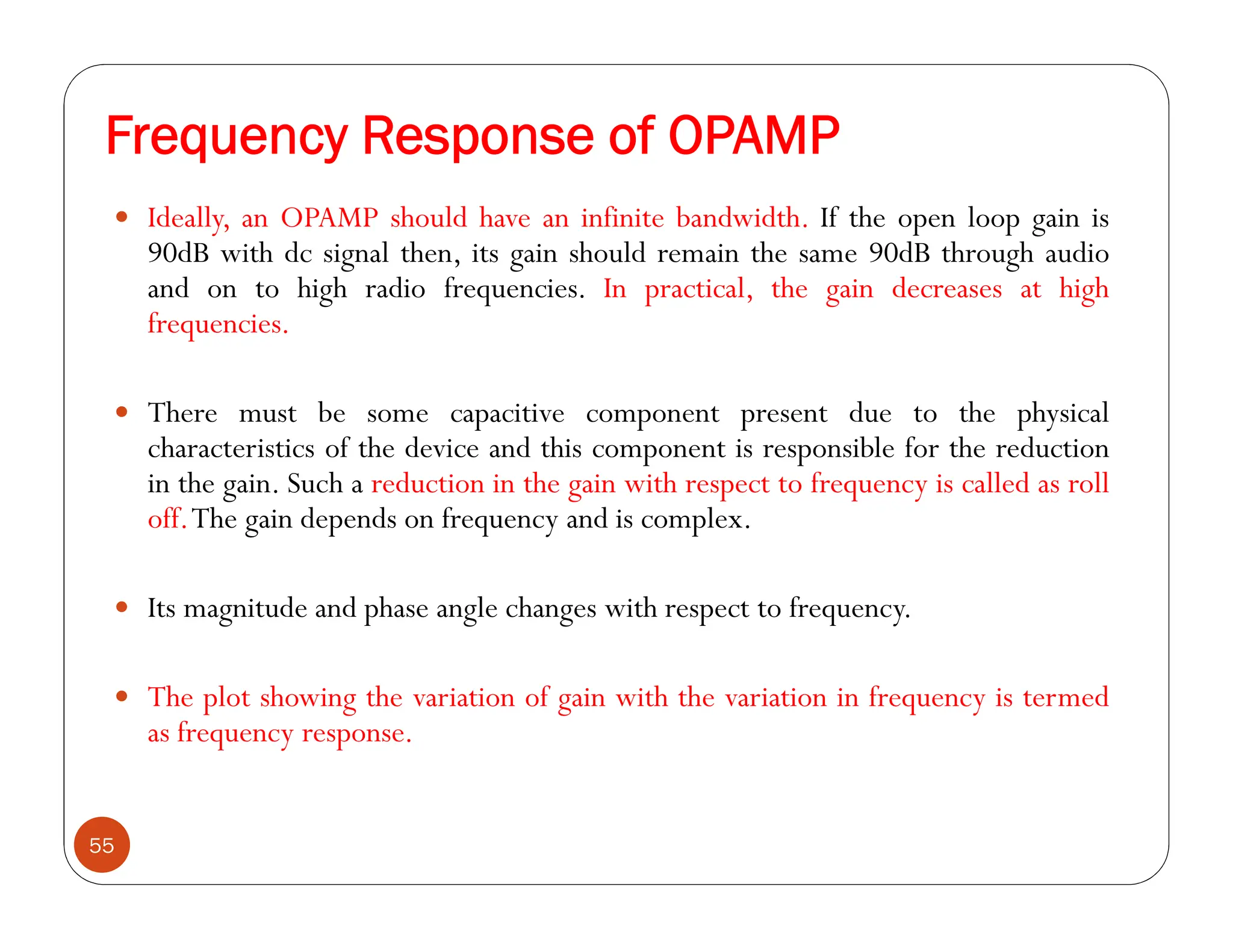
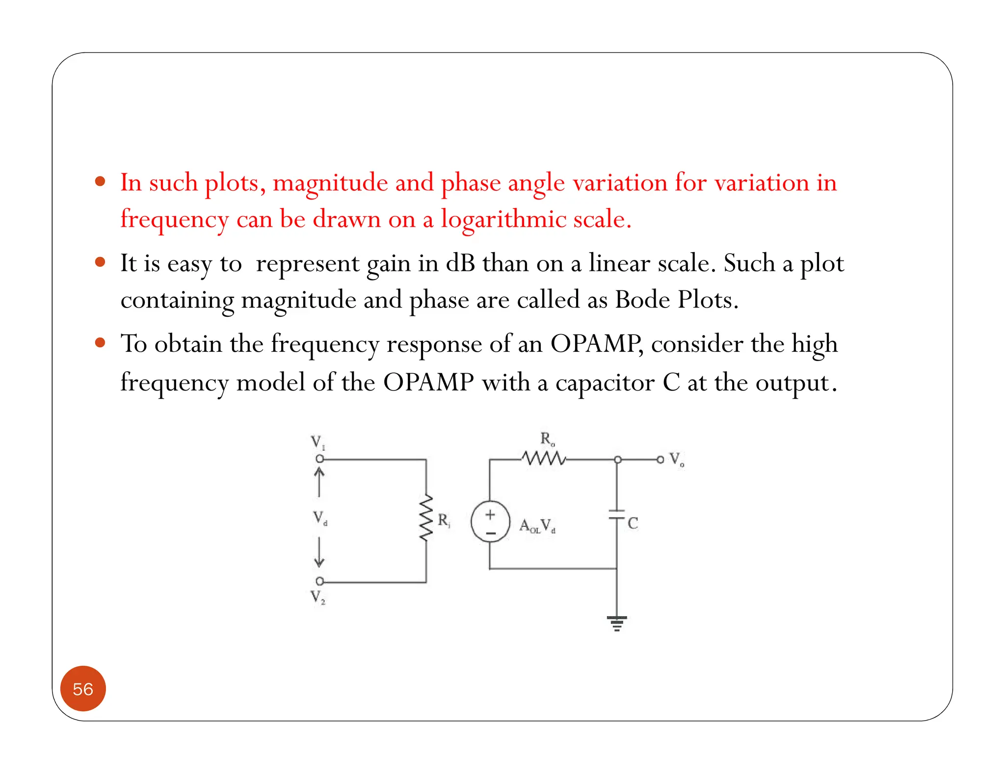
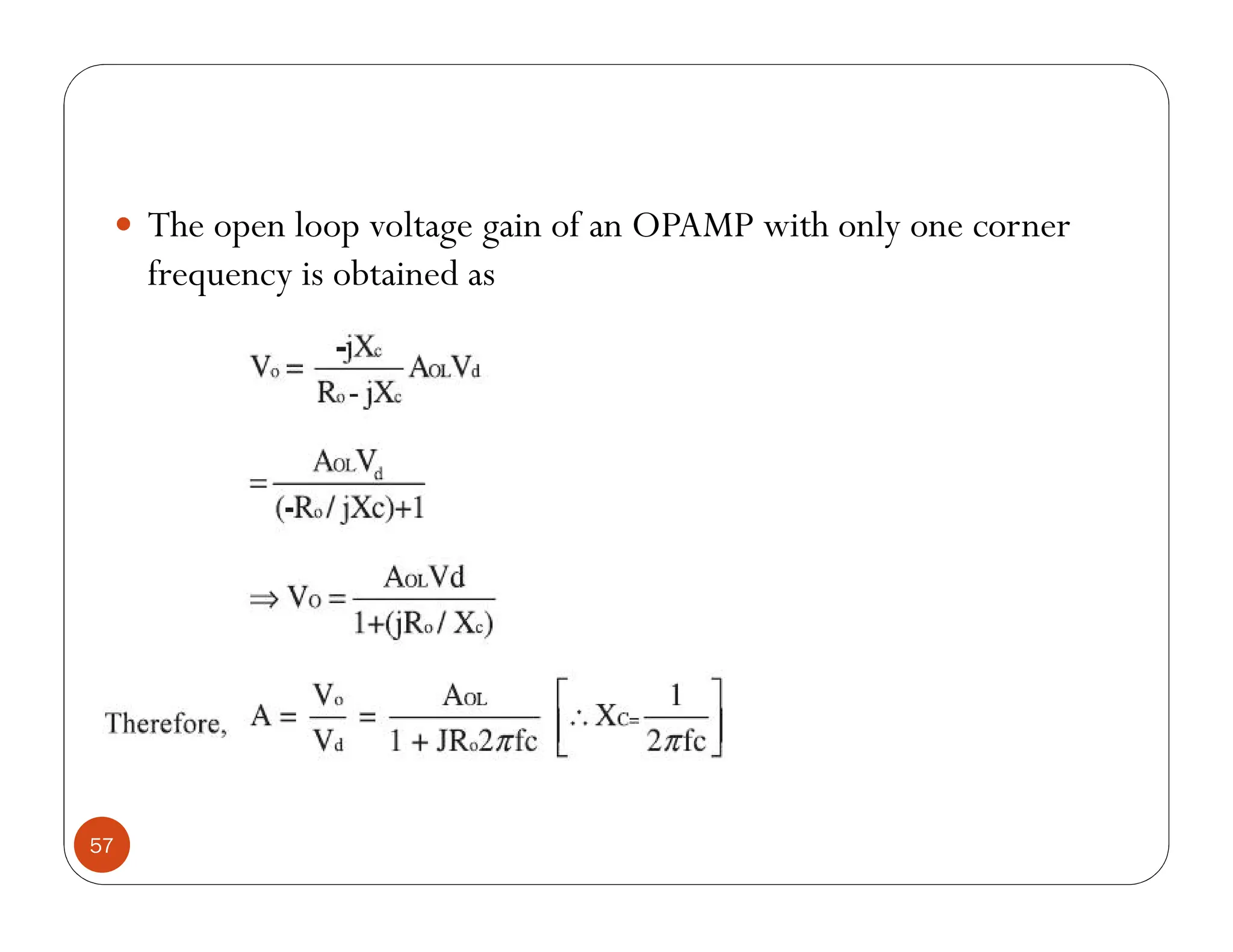
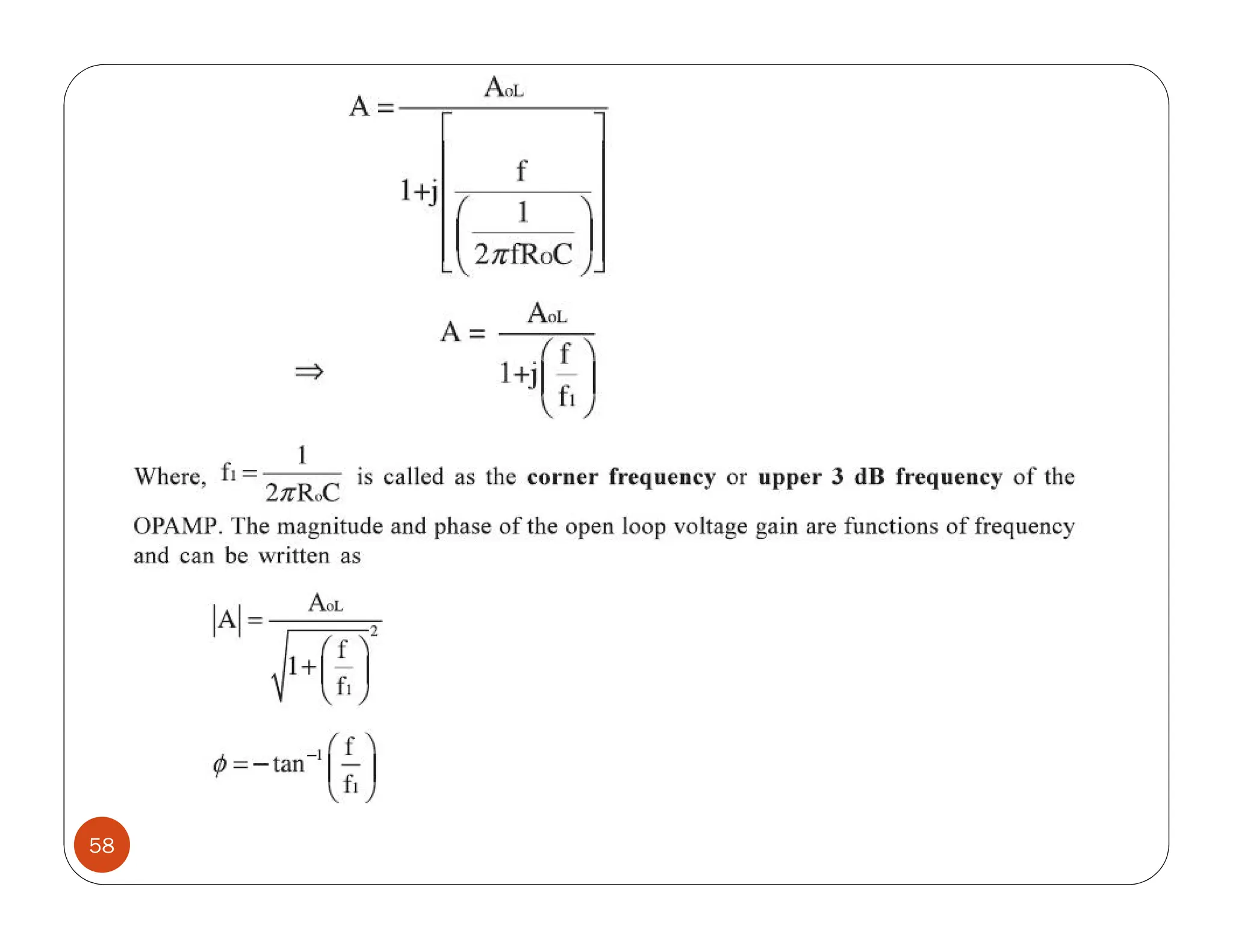
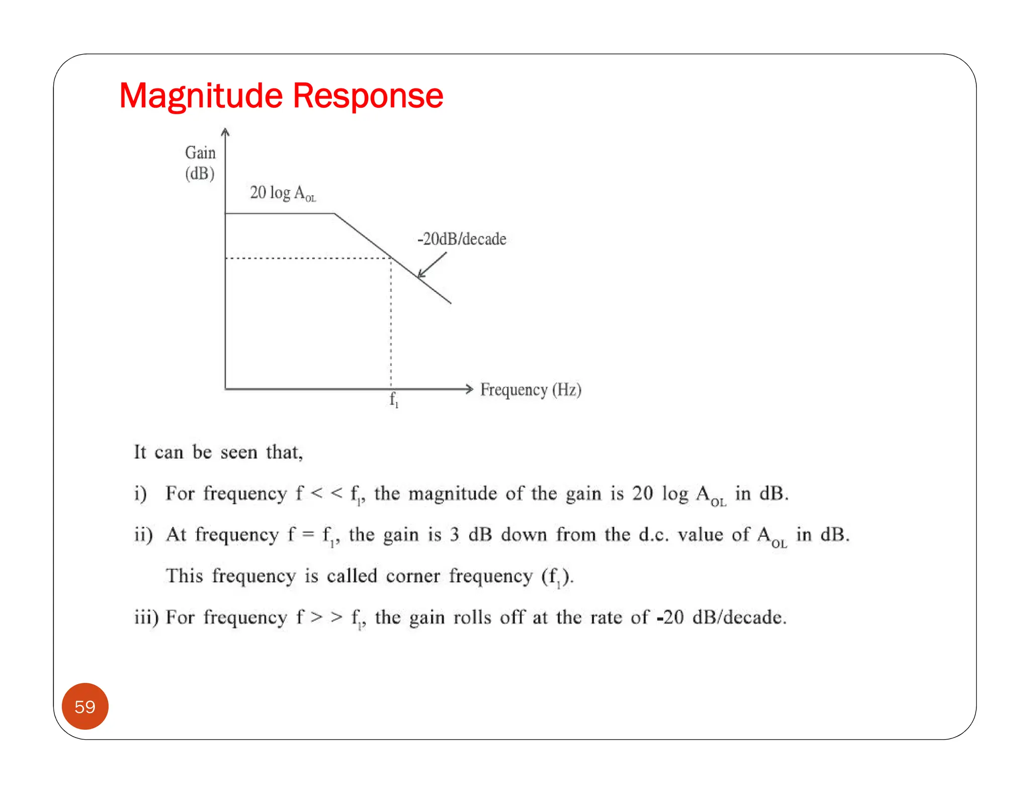
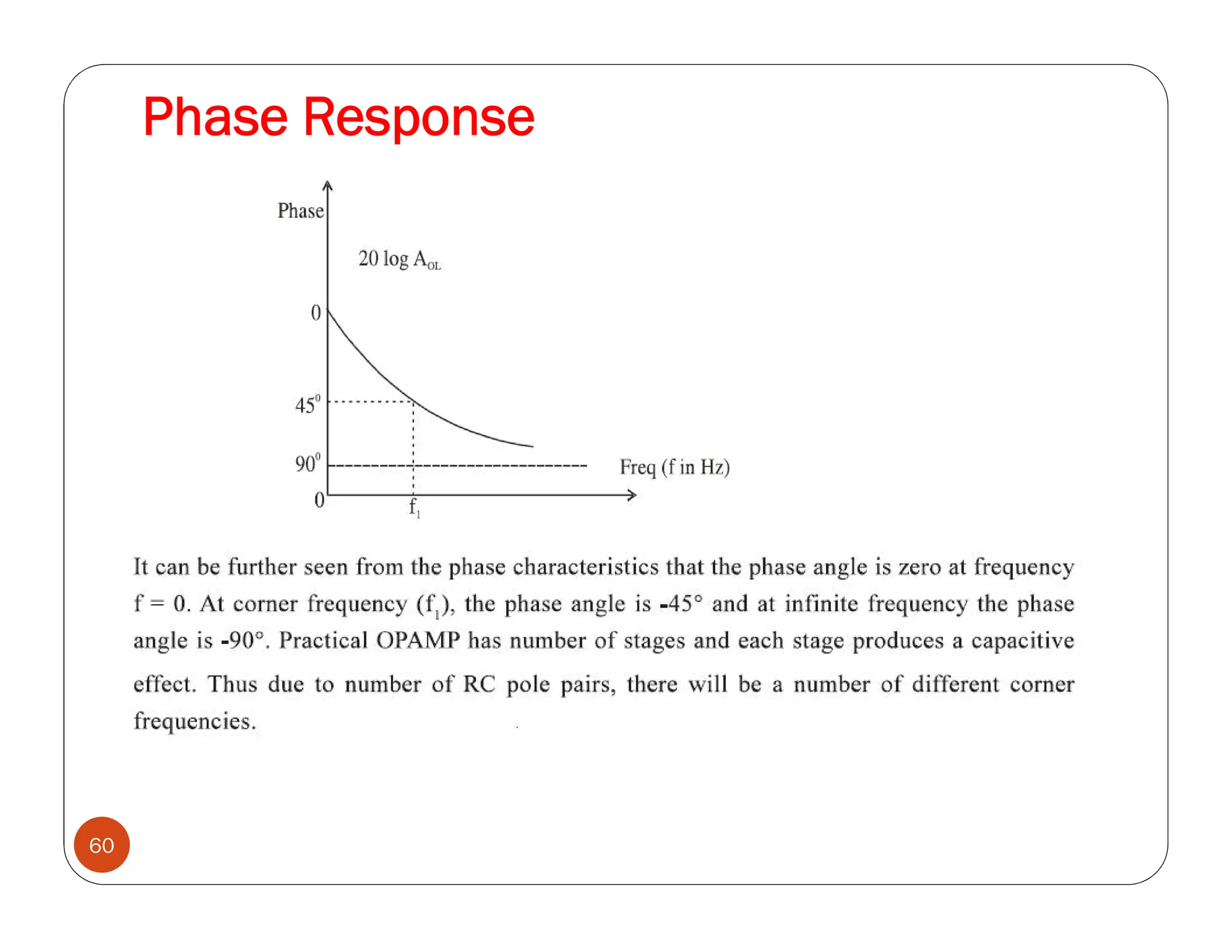
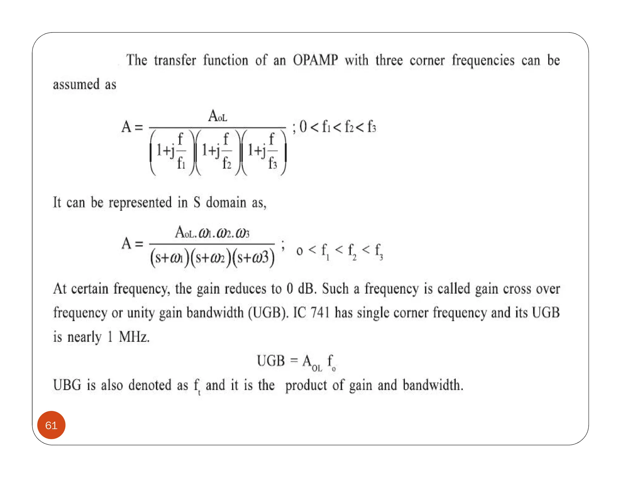
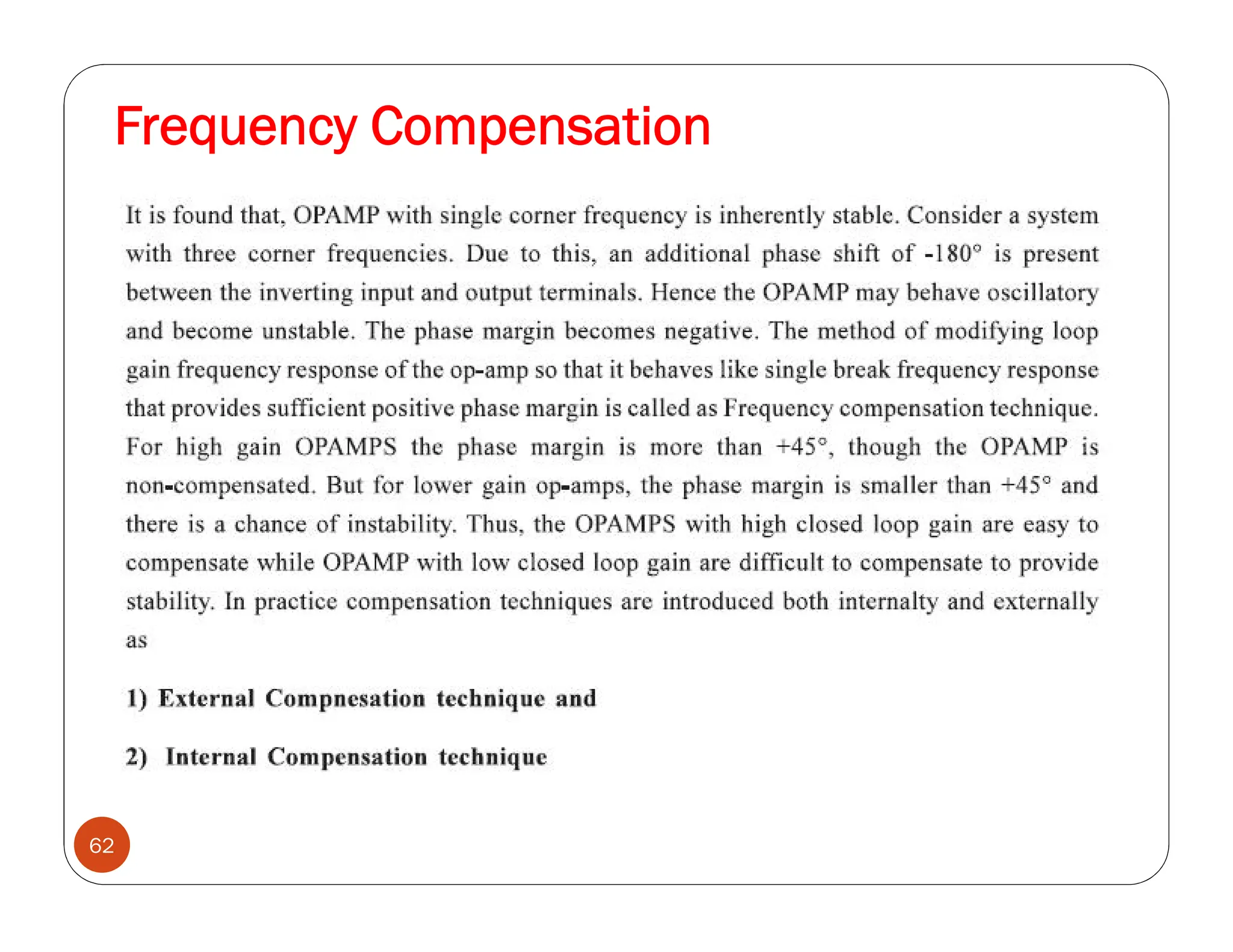
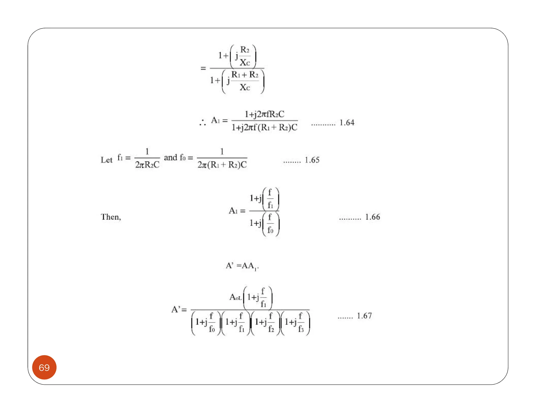
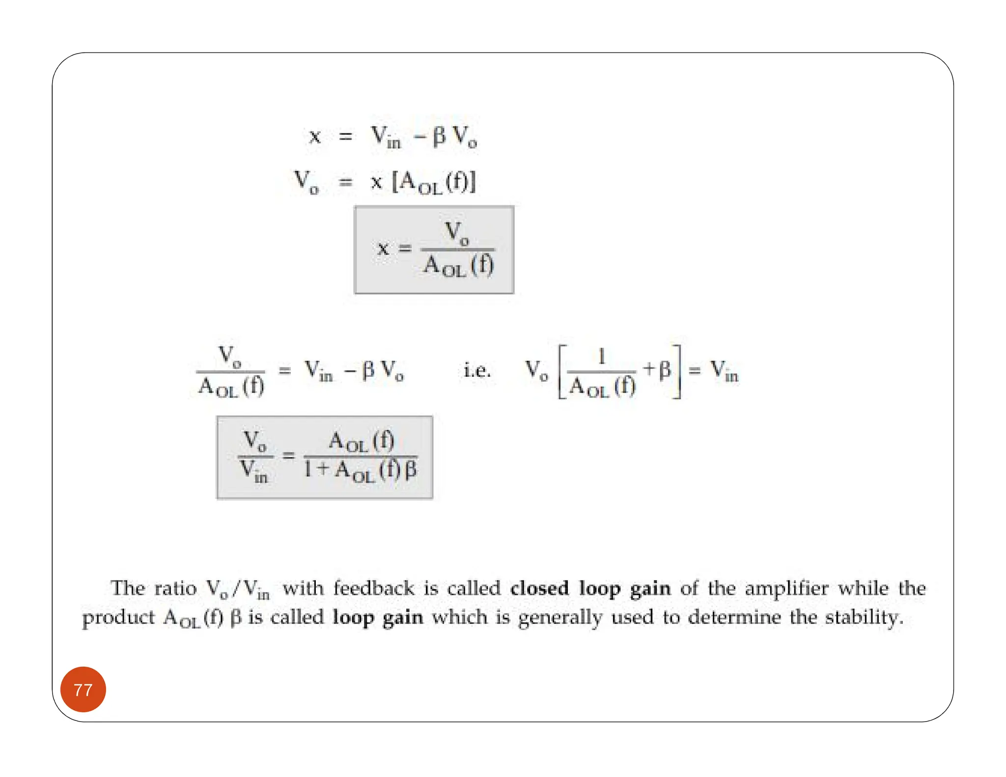
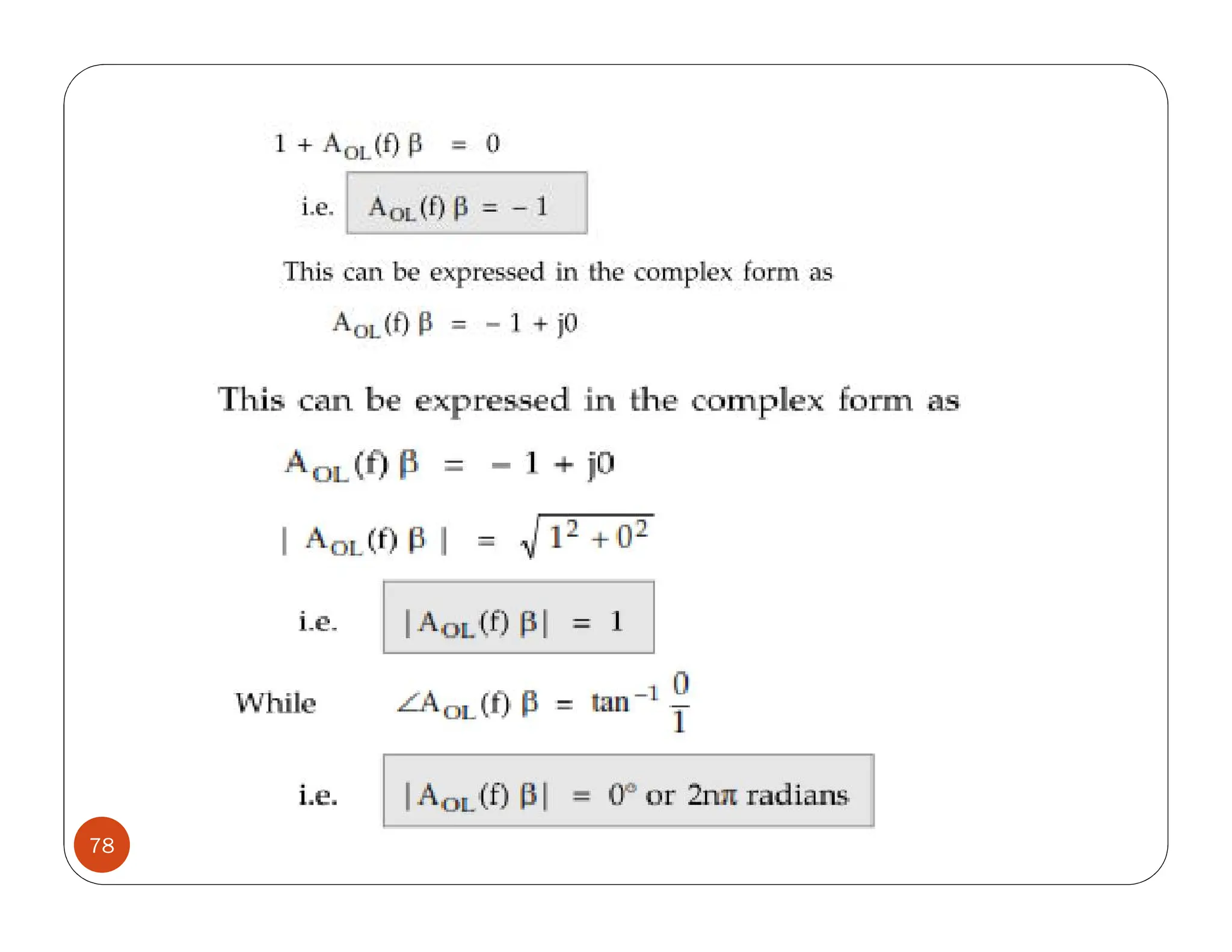
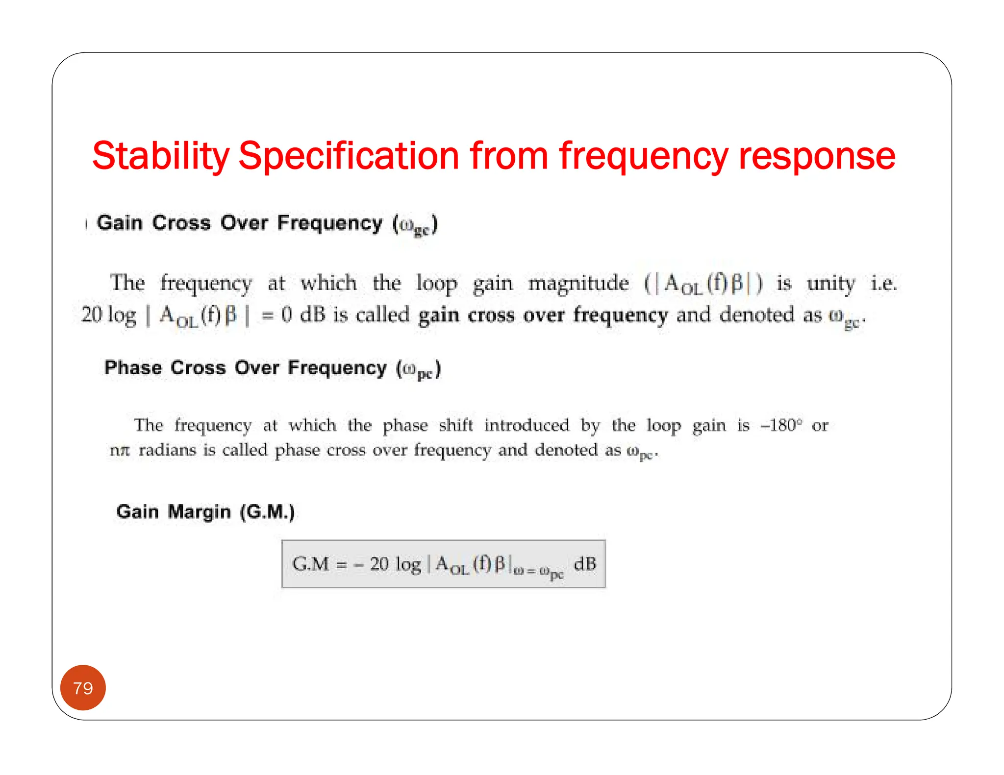
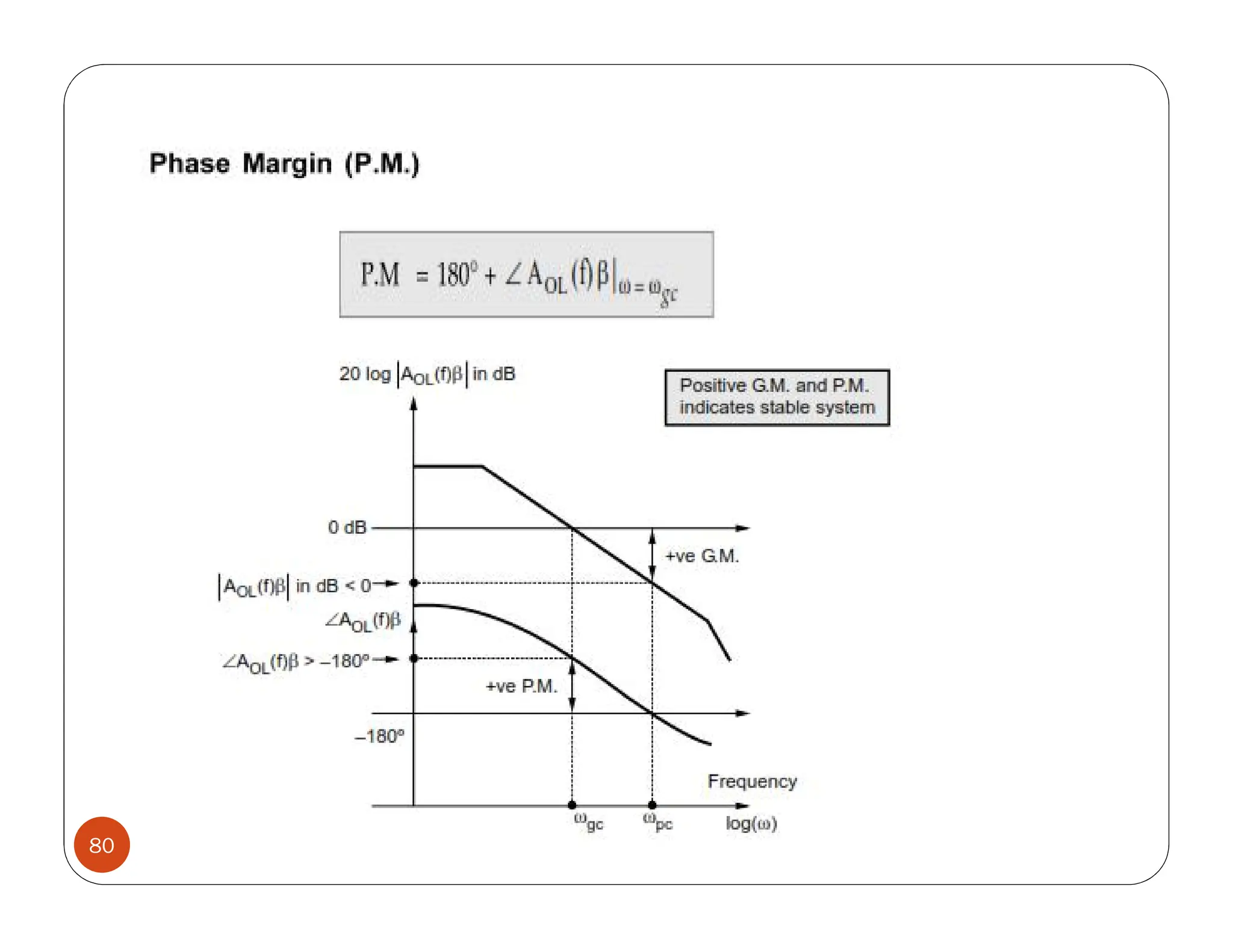
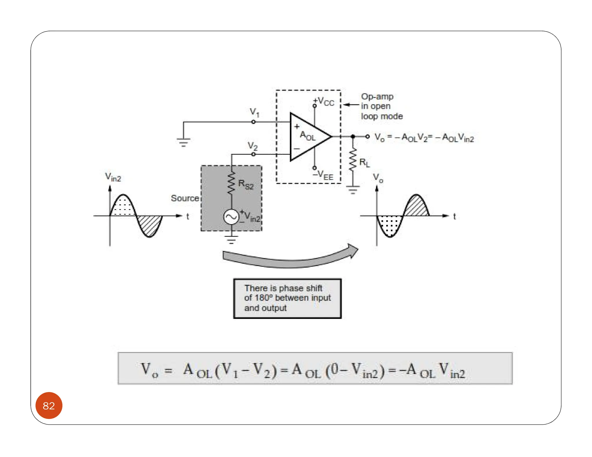
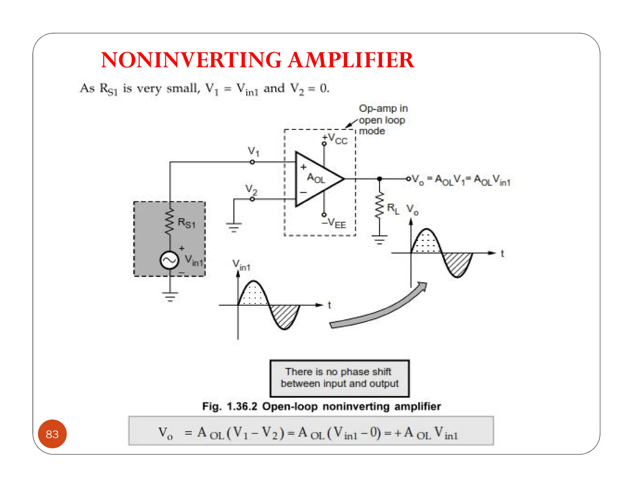
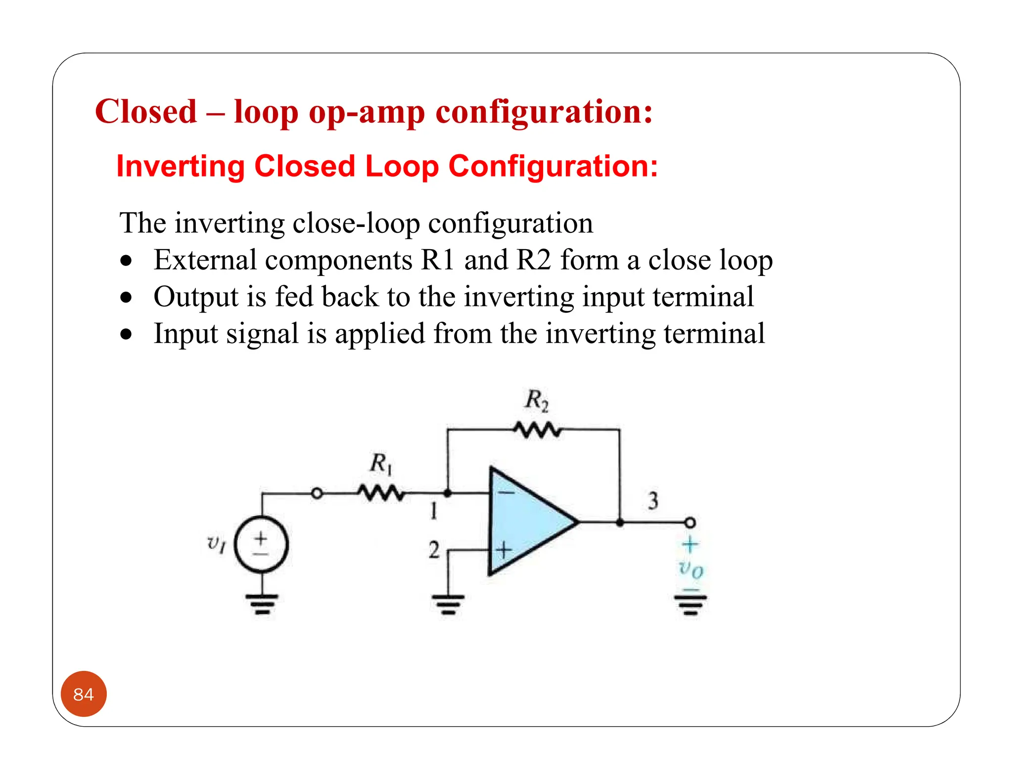
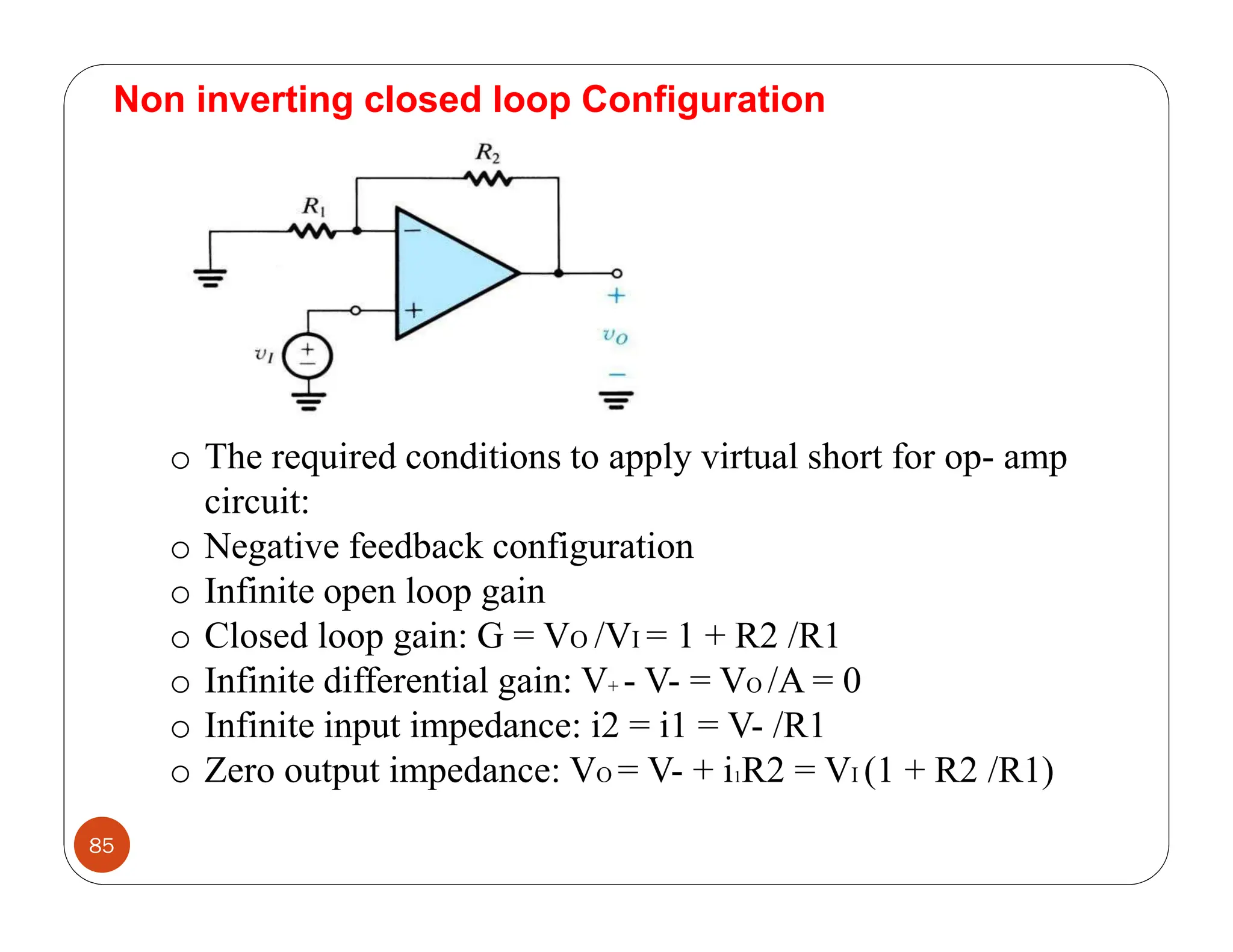
SlideShare a Scribd company logo
1 of 89
Download to read offline
UNIT – I
BASICS OF OPERATIONAL AMPLIFIERS
LINEAR INTEGRATED CIRCUITS
1
BASICS OF OPERATIONAL AMPLIFIERS
Syllabus
Current mirror and current sources, Current sources as active
loads, Voltage sources, Voltage References, BJT Differential
amplifier with active loads, Basic information about op-amps –
Ideal Operational Amplifier - General operational amplifier stages
-and internal circuit diagrams of IC 741, DC and AC performance
characteristics, slew rate, Open and closed loop configurations,
JFET operational amplifiers-LF 155 andTL082.
2
Integrated Circuit
3
 The integrated circuit or IC is a miniature, low cost electronic
circuit consisting of active and passive components that are
irreparably joined together on a single crystal chip of
silicon.
 Most of the components used in ICs are not similar to conventional
components in appearance although they perform similar electrical
functions.
Advantages of Integrated Circuit
4
1. Miniaturization and hence increased equipment density
2. Cost reduction due to batch processing
3. Increased system reliability due to elimination of soldered joints
4. Improved functional performance
5. Matched devices
6. Increased operating speeds (due to the absence of parasitic
capacitance effect)
7. Reduction in power consumption.
Classifications of ICs
5
6
Monolithic integrated circuits
 In monolithic integrated circuits, all circuit components, both active and
passive elements and their interconnections are manufactured into or on
top of a single chip of silicon.
 The monolithic circuit is ideal for applications where identical circuits
are required in very large quantities and hence provides lowest per-unit
cost and highest order of reliability.
Hybrid integrated circuits
 In hybrid circuits, separate component parts are attached to a ceramic
substrate and interconnected by means of either metallization pattern or
wire bonds. This technology is more adaptable to small quantity custom
circuits.
IC Chip Size
7
8
Amplifier
 An amplifier is an electronic device that can increase the power of
a signal (a time-varying voltage or current).
 It is a two-port electronic circuit that uses electric power from
a power supply to increase the amplitude of a signal applied to its
input terminals, producing a proportionally greater amplitude
signal at its output.
 The amount of amplification provided by an amplifier is measured
by its gain: the ratio of output voltage, current, or power to input.
 An amplifier is a circuit that has a power gain greater than one.
Operational amplifiers (op-amps)
9
 An operational amplifier is an amplifier circuit which typically has
very high open loop gain and differential inputs.
 Op amps have become very widely used as standardized "gain
blocks" in circuits due to their versatility; their gain, bandwidth
and other characteristics can be controlled by feedback through an
external circuit.
Introduction to OPAMP
10
 Linear Integrated Circuits are being used in a number of applications
such as in audio and radio communication, medical electronics,
instrumentation and control etc.
 An important linear IC is the OperationalAmplifier (OPAMP)
introduced in 1940s.
 Robert JWidlar at Fairchild brought out the popular OPAMP IC 741
between 1964 and 1968.
 It uses BJTs and FETs fabricated along with other components on a
single chip of silicon.
Introduction to OPAMP
11
 The OPAMP is a multi terminal device that has complex internal
circuitry.
 OPAMP's performance can be described by its terminal characteristics
and those external components that are connected to it.
 ICs have now become an integral part of all electronic circuits and work
at even low voltages. Its cost is also low due to bulk production.
 Due to the low cost, small size, versatility, flexibility and dependability
of OPAMPs they are used in the fields of process control,
communication, computers and measuring devices.
OPAMP-Symbols and terminals
12
 The input and output are in antiphase having 180 degree phase
difference.
Power Supply Connection
13
 TheV+ andV- power supply terminals are connected to two dc voltage sources.The
V+ pin is connected to the positive terminal of one source and theV- pin is connected
to the negative terminal of the other source as illustrated in figure where the two
sources are 15V batteries each.
 These are typical values, but in general, the power supply voltage may range from
about + 5V to + 22V. The common terminal of theV+ andV- sources is connected to
a reference point or ground.
14
Packages
15
The three popular packages available for OPAMP's.
1. Metal Can (TO) package
2. Dual in line package (DIP) and
3. Flat package
 Typical packages may have 8 terminals (TO or DIP), 10 terminals (Flat
pack) and 14 terminals (DIP and Flat pack).
 The widely used op-amp uA 741 consist of a single OPAMP and available as
8 pin DIP/Can or 14 pin DIP or 10 pin Metal Can package.
 The OPAMP works with a dual power supply. Both of them are dc and
generally balanced with +Vcc and -VEE Commercially used supply is ± 15V
or ± 12V
16
17
Manufacturer
18
 Some linear ICs are available in different versions such asA, C, E, S and SC. For example the
741, 741A, 741C, 741E, 741S and 741SC are different versions of the same OPAMP.
 The 741S and 741SC are military grade OPAMPs whose operating range is -55°C to 125°C
and have better slew rate compared to 741 and 741C.
 The 741C is commercial grade OPAMP whose operating range is 0°C to 75°C. 741E and 741C
are improved versions having better electrical specifications.
Block Diagram
19
Input Stage
 The input stage requires high input impedance to avoid the loading of sources. It is
a dual input, balanced output differential amplifier.This stage provides most of the
voltage gain of the amplifier. It also requires low output impedance.
Intermediate stage
 This is also a differential amplifier stage driven by the output of the first stage. It
has dual input, unbalanced (single ended) output.As direct coupling is used, the dc
voltage at the output of this stage is well above ground potential.This stage also
provides additional gain.
 Practically the intermediate stage is a cascade of amplifiers called Multistage
Amplifier.
Block Diagram
20
Buffer and Level Shifting Stage
 All the stages are directly coupled to each other.The dc quiescent voltage level of
previous stage gets directly applied as the input to the next stage.
 Therefore, stage by stage dc level increases well above the ground potential.These dc
voltages drive the transistor into saturation and cause distortion in the output due to
clipping.
 Hence, before the output stage, it is necessary to reduce such a high de voltage level to
zero volts with respect to ground.
 The buffer is usually an emitter follower whose input impedance is very high.This
prevents loading of the high gain stages.
Block Diagram
21
Output Stage
 The output stage must have a low output impedance, large ac output
voltage swing and high current sourcing and sinking capability.
 A push-pull complementary amplifier meets all these requirements and
it is used as the output stage.This stage also raises the current supplying
capability of the op-amp.
Ideal Operational Amplifier
22
1.An ideal OPAMP draws no current at both the inputs i.e. I1 =12 = 0.
Thus, the input impedance tends to infinity and no loading effect on the
driver stage.
2.The gain of the ideal OPAMP is infinite.Therefore, the differential input
V1-V2, =Vd is essentially zero for a finite output voltage.
3.The output is independent of the current drawn from either of the input
terminals. Its output impedance is zero and hence can able drive number of
output stages.
23
The ideal characteristics of OPAMP are :
1. Infinite voltage gain
2. Infinite input impedance
3. Zero output impedance
4. Infinite CMRR
5. Infinite slew rate
6. Zero offset voltage
7. Infinite bandwidth and
8. Zero Power Supply Rejection Ratio (PSRR)
24
OffsetVoltage
 The presence of the small output voltage thoughV1-V2 = 0 is called as
OffsetVoltage. It is zero for ideal op-amp ensuring zero output for zero
input voltage.
Infinite BandWidth
 The range of frequency over which the amplifier performance is
satisfactory is called as Bandwidth.
 For ideal case, it is infinity ensuring that the gain of the op-amp will be
constant over the frequency range from dc to infinity.That is, the OPAMP
can amplify both d.c. and ac signals.
Infinite CMRR
 The ability of the OPAMP to reject the common mode signals is called as
Common Mode Rejection Ratio (CMRR).
 It is the ratio of differential mode gain to common mode gain.
 Infinite CMRR ensures zero common mode gain.Therefore, common
mode noise output voltage is zero for an ideal OPAMP.
25
Infinite Slew rate (S = 0)
 This ensures that, the changes in output voltage occurs simultaneously
with the changes in the input voltage. If the input changes, output must
also change accordingly. If this is not met then distortion occurs.
 Slew rate is defined as the maximum rate of change of output voltage
with time and expressed inV/us.
Zero PSRR
 Power Supply Rejection Ratio (PSRR) is defined as the ratio of input
offset voltage due to change in supply voltage producing it.
 IfVEE is constant andVcc alone changes, then PSRR can be defined as,
VOLTAGE TRANSFER CURVE OF OPAMP
26
 The graph of output voltage V0 plotted against the differential input voltage Vd
keeping the gain constant is called as Voltage Transfer Characteristic curve of an
OPAMP.
Ideal voltage transfer curve
 Ideally the open loop gain of an OPAMP is infinity.Also,V0. =AOL Vd.Thus, for
zero input voltage the output voltage is always at a saturation level of ±Vsat due
to infinite gain.
27
Practical voltage transfer curve
Inverting Amplifier
28
 An amplifier which provides a phase shift of
180° between the input and the output is
called as inverting amplifier.
 When the input signalVi is applied to the
inverting terminal (-ve terminal) of the
OPAMP, an input current Ii starts to flow in
to the OPAMP.
 For an ideal OPAMP, the input impedance is
infinity and the point X is at at virtual
ground potential.
 Therefore, the input current Ii, will not flow
into the OPAMP and it will flow through the
feedback resister Rf with respect to the
virtual ground point X.
Inverting Amplifier
29
30
Non-Inverting Amplifier
31
 The input signal is amplified without any phase inversion.
 The input signalVi is applied to the non-inverting terminal (+ve terminal) of
the OPAMP. Since the point X is at virtual ground.
Ii = If
32
Voltage Follower
33
 Voltage follower is a unity gain amplifier and it has very
large input impedance.As the name implies, the output
follows the input.
 In this circuit, the input resistor (Ri) and feedback resistor
(Rf) are removed.The inverting terminal is connected or
shorted with the output terminal.
 Due to the existence of virtual short circuit at the input
side, the voltage available at the inverting terminal is equal
toVi.
 Therefore, the output voltage is equal to the
input voltage (Vo=Vi)
 Whenever there is a change in input voltageVi, that will
be followed in the output voltage (Vo).
Differential Amplifier
34
 A circuit that amplifies the difference between two signals is called a
difference or differential amplifier.This type of the amplifier is very
useful in instrumentation circuits.
 Since, the differential voltage at the input terminals of the op-amp is
zero, nodes 'a' and b' are at the same potential, designated asV3.
35
Subtracting Eq.(4) from (3) Such a circuit is very useful in detecting very
small difference in signals, since the gain R2/ R1
can be chosen to be very large. For example, if
R2= 100 R1, then a small differenceV1-V2 is
amplified 100 times.
Difference-mode and common-mode gains
36
 If,V1=V2, thenV0 = 0.That is, the signal common to both inputs gets cancelled
and produces no output voltage.This is true for an ideal op-amp, however, a
practical op-amp exhibits some small response to the common mode
component of the input voltages too.
 For example, the outputV0 will have different value for case (i) withV1 = 100
µV andV2 = 50 µV and case (ii) withV1= 1000 µV andV2 = 950 µV, even
though the difference signalV1-V2= 50 µV in both the cases.The output voltage
depends not only upon the difference signalVd at the input, but is also affected
by the average voltage of the input signals, called the common-mode signalVCM
defined as,
37
For differential amplifier, the gain at the output with respect to the positive
terminal is slightly different in magnitude to that of the negative terminal.
So, even with the same voltage applied to both inputs, the output is not zero.
The output, therefore, must be ex-pressed as,
38
 The relative sensitivity of an op-amp to a difference signal as compared
to a common-mode signal is called common-mode rejection ratio
(CMRR) and gives the figure of merit p for the differential amplifier.
 So, CMRR is given by:
and is usually expressed in decibels (dB).
 For example, the µA741 op-amp has a minimum CMRR of 70 dB
whereas a precision op-amp such as µA725A has a minimum CMRR of
120 dB. Clearly, we should haveADM large andAcm should be zero ideally.
So, higher the value of CMRR, better is the op-amp.
COMMON-MODE REJECTION RATIO
DC CHARACTERISTICS OF OP-AMP
39
 An ideal op-amp draws no current from the source and its
response is also independent of temperature. However, a real op-
amp does not work in this way. Current is taken from the source
into the op-amp inputs.Also the two inputs respond differently to
current and voltage due to mismatch in transistor.
 A real op-amp also shifts its operation with temperature.These
non-ideal dc characteristics that add error components to the dc
output voltage are
• Input bias current
• Input offset current
• Input offset voltage
•Thermal drift
1.Input bias current
40
 Practically, input terminals do conduct a small value of dc current to bias the
input transistors.The base currents entering into the inverting and non-
inverting terminals are IB
- and IB
+ respectively as shown in the figure
 Even though both the transistors are identical, IB
- and IB
+ are not exactly equal
due to the internal imbalance between the two inputs. Manufacturers specify
the input bias current IB as the average value of the base currents entering into
the terminals of an op-amp.Therefore,
41
42
43
44
2.Input offset current
45
Input offset voltage
46
 In spite of the use of the above compensating techniques, it is
found that the output voltage may still not be zero with zero input
voltage.
 This is due to unavoidable imbalances inside the op-amp and one
may have to apply a small voltage at the input terminal to make
output (V0) = 0.This voltage is called input offset voltageVos.
 This is the voltage required to be applied at the input for making
output voltage to zero (V0 = 0).
Total output offset voltage
47
 The total output offset voltageVOT could be either more or less
than the offset voltage produced at the output due to input bias
current (IB) or input offset voltage alone(VOS) because IB andVOS
could be either positive or negative with respect to ground.
 Therefore, the maximum offset voltage at the output of an
inverting and non-inverting amplifier without any compensation
technique provide offset compensation pins to nullify the offset
voltage.
48
 A 10K potentiometer is placed across offset null pins 1&5.The
wipes connected to the negative supply at pin 4.The position of the
wipes is adjusted to nullify the offset voltage.
 When the given op-amps does not have these offset null pins,
external balancing techniques are used as shown in figure.
49
Thermal drift
50
 Bias current, offset current and offset voltage change with
temperature.A circuit carefully nulled at 25°C may not remain so
when the temperature rises to 35°C.This is called drift.
 Offset current drift is expressed in nA/°C.This indicate the
change in offset for each degree Celsius change in temperature.
 Techniques to avoid drift: Careful printed circuit board layout
must be used to keep op-amps away from source of heat.
 Forced air cooling may be used to stabilize the ambient
temperature.
AC Characteristics of OPAMP
51
1. Slew Rate
2. Frequency response
Slew Rate
 It is defined as the maximum rate of change of output voltage with
time. It is expressed inV/µsec.The slew rate S is given by,
 The slew rate is caused due to the charging rate of the
compensating capacitor, current limiting capability and saturation
of the internal stages of the OPAMP, when a high frequency large
amplitude signal is applied.
Slew Rate
52
 The internal capacitor voltage cannot change instantaneously.
 For large charging rate, the capacitor should be small or charging current
must be large. Hence, the slew rate of an OPAMP whose maximum
internal capacitor charging current is known can be found using the
formula,
 For IC741, the charging current is 15 µA and the internal capacitance is
30 pF. Therefore the slew rate is 0.5V/µsec. Ideally, it should be infinite.
 Higher the value of S, better is the OPAMP performance.
Slew Rate Equation
53
54
Frequency Response of OPAMP
55
 Ideally, an OPAMP should have an infinite bandwidth. If the open loop gain is
90dB with dc signal then, its gain should remain the same 90dB through audio
and on to high radio frequencies. In practical, the gain decreases at high
frequencies.
 There must be some capacitive component present due to the physical
characteristics of the device and this component is responsible for the reduction
in the gain. Such a reduction in the gain with respect to frequency is called as roll
off.The gain depends on frequency and is complex.
 Its magnitude and phase angle changes with respect to frequency.
 The plot showing the variation of gain with the variation in frequency is termed
as frequency response.
56
 In such plots, magnitude and phase angle variation for variation in
frequency can be drawn on a logarithmic scale.
 It is easy to represent gain in dB than on a linear scale. Such a plot
containing magnitude and phase are called as Bode Plots.
 To obtain the frequency response of an OPAMP, consider the high
frequency model of the OPAMP with a capacitor C at the output.
57
 The open loop voltage gain of an OPAMP with only one corner
frequency is obtained as
58
Magnitude Response
59
Phase Response
60
61
Frequency Compensation
62
External Compensation Technique
63
Dominant Pole Compensation
64
65
66
Pole Zero Compensation
67
68
69
70
Feed Forward Compensation
71
72
Internal Compensation
73
74
75
Stability of OPAMP
76
77
78
79
Stability Specification from frequency response
80
OPEN LOOP CONFIGURATION OF OPAMP
81
INVERTING AMPLIFIER
82
83
NONINVERTING AMPLIFIER
84
Closed – loop op-amp configuration:
The inverting close-loop configuration
 External components R1 and R2 form a close loop
 Output is fed back to the inverting input terminal
 Input signal is applied from the inverting terminal
Inverting Closed Loop Configuration:
85
Non inverting closed loop Configuration
o The required conditions to apply virtual short for op- amp
circuit:
o Negative feedback configuration
o Infinite open loop gain
o Closed loop gain: G = VO /VI = 1 + R2 /R1
o Infinite differential gain: V+ - V- = VO /A = 0
o Infinite input impedance: i2 = i1 = V- /R1
o Zero output impedance: VO = V- + i1R2 = VI (1 + R2 /R1)
JFET Operational Amplifiers– LF155
86
 FEATURES
 Guaranteed OffsetVoltage Drift on
All Grades.
 Guaranteed Slew Rate onAll
Grades.

 Guaranteed Low Input Offset
Current 10pA Max.
 Guaranteed Low Input Bias
Current 50pA Max.
 Guaranteed High Slew Rate
(156A/356A) 10V/µs Min.
 Fast Settling to 0.01% 1.5µS.
87
Applications:
 Precision high speed integrators
 Fast D/A and A/D converters
 High impedance buffers Wideband, low noise, low drift
amplifiers
 Logarithmic amplifiers
TL082 JFET OP-AMP
88
 FEATURES
APPLICATIONS
89

More Related Content

Similar to EC3451 LINEAR INTEGRATED CIRCUITS UNIT 1 .pdf

Similar to EC3451 LINEAR INTEGRATED CIRCUITS UNIT 1 .pdf (20)

Operational%20 amplifier
Operational%20 amplifierOperational%20 amplifier
Operational%20 amplifier
 
Op-amp & its characteristics
Op-amp  & its characteristics Op-amp  & its characteristics
Op-amp & its characteristics
 
Operational amplifier
Operational amplifierOperational amplifier
Operational amplifier
 
Op amp
Op ampOp amp
Op amp
 
An operational amplifier for merge
An operational amplifier   for mergeAn operational amplifier   for merge
An operational amplifier for merge
 
Electronic circuit design lab manual
Electronic circuit design lab manualElectronic circuit design lab manual
Electronic circuit design lab manual
 
battery charging circuits
battery charging circuitsbattery charging circuits
battery charging circuits
 
OP-AMP(OPERATIONAL AMPLIFIER)BE
OP-AMP(OPERATIONAL AMPLIFIER)BEOP-AMP(OPERATIONAL AMPLIFIER)BE
OP-AMP(OPERATIONAL AMPLIFIER)BE
 
Op-amp.pptx
Op-amp.pptxOp-amp.pptx
Op-amp.pptx
 
Operating Amplifier
Operating AmplifierOperating Amplifier
Operating Amplifier
 
Op amp basics
Op amp basicsOp amp basics
Op amp basics
 
L9 opamp
L9 opampL9 opamp
L9 opamp
 
Op amp
Op ampOp amp
Op amp
 
Ec6412 linear-integrated-circuit-laboratory
Ec6412 linear-integrated-circuit-laboratoryEc6412 linear-integrated-circuit-laboratory
Ec6412 linear-integrated-circuit-laboratory
 
Opertional amplifier khiri elrmali libya
Opertional amplifier khiri elrmali  libyaOpertional amplifier khiri elrmali  libya
Opertional amplifier khiri elrmali libya
 
A Study on High Precision Op-Amps
A Study on High Precision Op-AmpsA Study on High Precision Op-Amps
A Study on High Precision Op-Amps
 
ANALYSIS ON CLASS-A VOLTAGE FOLLOWER
ANALYSIS ON CLASS-A VOLTAGE FOLLOWERANALYSIS ON CLASS-A VOLTAGE FOLLOWER
ANALYSIS ON CLASS-A VOLTAGE FOLLOWER
 
Analog circuit Unit 2.ppt
Analog circuit Unit 2.pptAnalog circuit Unit 2.ppt
Analog circuit Unit 2.ppt
 
chapter 3_bem.pptx
chapter 3_bem.pptxchapter 3_bem.pptx
chapter 3_bem.pptx
 
Integrated circuit
Integrated circuitIntegrated circuit
Integrated circuit
 

Recently uploaded

HARMONY IN THE NATURE AND EXISTENCE - Unit-IV
HARMONY IN THE NATURE AND EXISTENCE - Unit-IVHARMONY IN THE NATURE AND EXISTENCE - Unit-IV
HARMONY IN THE NATURE AND EXISTENCE - Unit-IVRajaP95
 
(ANVI) Koregaon Park Call Girls Just Call 7001035870 [ Cash on Delivery ] Pun...
(ANVI) Koregaon Park Call Girls Just Call 7001035870 [ Cash on Delivery ] Pun...(ANVI) Koregaon Park Call Girls Just Call 7001035870 [ Cash on Delivery ] Pun...
(ANVI) Koregaon Park Call Girls Just Call 7001035870 [ Cash on Delivery ] Pun...ranjana rawat
 
IVE Industry Focused Event - Defence Sector 2024
IVE Industry Focused Event - Defence Sector 2024IVE Industry Focused Event - Defence Sector 2024
IVE Industry Focused Event - Defence Sector 2024Mark Billinghurst
 
Decoding Kotlin - Your guide to solving the mysterious in Kotlin.pptx
Decoding Kotlin - Your guide to solving the mysterious in Kotlin.pptxDecoding Kotlin - Your guide to solving the mysterious in Kotlin.pptx
Decoding Kotlin - Your guide to solving the mysterious in Kotlin.pptxJoão Esperancinha
 
Architect Hassan Khalil Portfolio for 2024
Architect Hassan Khalil Portfolio for 2024Architect Hassan Khalil Portfolio for 2024
Architect Hassan Khalil Portfolio for 2024hassan khalil
 
College Call Girls Nashik Nehal 7001305949 Independent Escort Service Nashik
College Call Girls Nashik Nehal 7001305949 Independent Escort Service NashikCollege Call Girls Nashik Nehal 7001305949 Independent Escort Service Nashik
College Call Girls Nashik Nehal 7001305949 Independent Escort Service NashikCall Girls in Nagpur High Profile
 
main PPT.pptx of girls hostel security using rfid
main PPT.pptx of girls hostel security using rfidmain PPT.pptx of girls hostel security using rfid
main PPT.pptx of girls hostel security using rfidNikhilNagaraju
 
Microscopic Analysis of Ceramic Materials.pptx
Microscopic Analysis of Ceramic Materials.pptxMicroscopic Analysis of Ceramic Materials.pptx
Microscopic Analysis of Ceramic Materials.pptxpurnimasatapathy1234
 
Gfe Mayur Vihar Call Girls Service WhatsApp -> 9999965857 Available 24x7 ^ De...
Gfe Mayur Vihar Call Girls Service WhatsApp -> 9999965857 Available 24x7 ^ De...Gfe Mayur Vihar Call Girls Service WhatsApp -> 9999965857 Available 24x7 ^ De...
Gfe Mayur Vihar Call Girls Service WhatsApp -> 9999965857 Available 24x7 ^ De...srsj9000
 
Study on Air-Water & Water-Water Heat Exchange in a Finned Tube Exchanger
Study on Air-Water & Water-Water Heat Exchange in a Finned Tube ExchangerStudy on Air-Water & Water-Water Heat Exchange in a Finned Tube Exchanger
Study on Air-Water & Water-Water Heat Exchange in a Finned Tube ExchangerAnamika Sarkar
 
CCS355 Neural Network & Deep Learning UNIT III notes and Question bank .pdf
CCS355 Neural Network & Deep Learning UNIT III notes and Question bank .pdfCCS355 Neural Network & Deep Learning UNIT III notes and Question bank .pdf
CCS355 Neural Network & Deep Learning UNIT III notes and Question bank .pdfAsst.prof M.Gokilavani
 
Internship report on mechanical engineering
Internship report on mechanical engineeringInternship report on mechanical engineering
Internship report on mechanical engineeringmalavadedarshan25
 
VIP Call Girls Service Hitech City Hyderabad Call +91-8250192130
VIP Call Girls Service Hitech City Hyderabad Call +91-8250192130VIP Call Girls Service Hitech City Hyderabad Call +91-8250192130
VIP Call Girls Service Hitech City Hyderabad Call +91-8250192130Suhani Kapoor
 
Call Girls Delhi {Jodhpur} 9711199012 high profile service
Call Girls Delhi {Jodhpur} 9711199012 high profile serviceCall Girls Delhi {Jodhpur} 9711199012 high profile service
Call Girls Delhi {Jodhpur} 9711199012 high profile servicerehmti665
 
High Profile Call Girls Nagpur Isha Call 7001035870 Meet With Nagpur Escorts
High Profile Call Girls Nagpur Isha Call 7001035870 Meet With Nagpur EscortsHigh Profile Call Girls Nagpur Isha Call 7001035870 Meet With Nagpur Escorts
High Profile Call Girls Nagpur Isha Call 7001035870 Meet With Nagpur Escortsranjana rawat
 
Model Call Girl in Narela Delhi reach out to us at 🔝8264348440🔝
Model Call Girl in Narela Delhi reach out to us at 🔝8264348440🔝Model Call Girl in Narela Delhi reach out to us at 🔝8264348440🔝
Model Call Girl in Narela Delhi reach out to us at 🔝8264348440🔝soniya singh
 
SPICE PARK APR2024 ( 6,793 SPICE Models )
SPICE PARK APR2024 ( 6,793 SPICE Models )SPICE PARK APR2024 ( 6,793 SPICE Models )
SPICE PARK APR2024 ( 6,793 SPICE Models )Tsuyoshi Horigome
 

Recently uploaded (20)

9953056974 Call Girls In South Ex, Escorts (Delhi) NCR.pdf
9953056974 Call Girls In South Ex, Escorts (Delhi) NCR.pdf9953056974 Call Girls In South Ex, Escorts (Delhi) NCR.pdf
9953056974 Call Girls In South Ex, Escorts (Delhi) NCR.pdf
 
HARMONY IN THE NATURE AND EXISTENCE - Unit-IV
HARMONY IN THE NATURE AND EXISTENCE - Unit-IVHARMONY IN THE NATURE AND EXISTENCE - Unit-IV
HARMONY IN THE NATURE AND EXISTENCE - Unit-IV
 
(ANVI) Koregaon Park Call Girls Just Call 7001035870 [ Cash on Delivery ] Pun...
(ANVI) Koregaon Park Call Girls Just Call 7001035870 [ Cash on Delivery ] Pun...(ANVI) Koregaon Park Call Girls Just Call 7001035870 [ Cash on Delivery ] Pun...
(ANVI) Koregaon Park Call Girls Just Call 7001035870 [ Cash on Delivery ] Pun...
 
IVE Industry Focused Event - Defence Sector 2024
IVE Industry Focused Event - Defence Sector 2024IVE Industry Focused Event - Defence Sector 2024
IVE Industry Focused Event - Defence Sector 2024
 
Decoding Kotlin - Your guide to solving the mysterious in Kotlin.pptx
Decoding Kotlin - Your guide to solving the mysterious in Kotlin.pptxDecoding Kotlin - Your guide to solving the mysterious in Kotlin.pptx
Decoding Kotlin - Your guide to solving the mysterious in Kotlin.pptx
 
Architect Hassan Khalil Portfolio for 2024
Architect Hassan Khalil Portfolio for 2024Architect Hassan Khalil Portfolio for 2024
Architect Hassan Khalil Portfolio for 2024
 
College Call Girls Nashik Nehal 7001305949 Independent Escort Service Nashik
College Call Girls Nashik Nehal 7001305949 Independent Escort Service NashikCollege Call Girls Nashik Nehal 7001305949 Independent Escort Service Nashik
College Call Girls Nashik Nehal 7001305949 Independent Escort Service Nashik
 
main PPT.pptx of girls hostel security using rfid
main PPT.pptx of girls hostel security using rfidmain PPT.pptx of girls hostel security using rfid
main PPT.pptx of girls hostel security using rfid
 
Microscopic Analysis of Ceramic Materials.pptx
Microscopic Analysis of Ceramic Materials.pptxMicroscopic Analysis of Ceramic Materials.pptx
Microscopic Analysis of Ceramic Materials.pptx
 
Exploring_Network_Security_with_JA3_by_Rakesh Seal.pptx
Exploring_Network_Security_with_JA3_by_Rakesh Seal.pptxExploring_Network_Security_with_JA3_by_Rakesh Seal.pptx
Exploring_Network_Security_with_JA3_by_Rakesh Seal.pptx
 
Gfe Mayur Vihar Call Girls Service WhatsApp -> 9999965857 Available 24x7 ^ De...
Gfe Mayur Vihar Call Girls Service WhatsApp -> 9999965857 Available 24x7 ^ De...Gfe Mayur Vihar Call Girls Service WhatsApp -> 9999965857 Available 24x7 ^ De...
Gfe Mayur Vihar Call Girls Service WhatsApp -> 9999965857 Available 24x7 ^ De...
 
Study on Air-Water & Water-Water Heat Exchange in a Finned Tube Exchanger
Study on Air-Water & Water-Water Heat Exchange in a Finned Tube ExchangerStudy on Air-Water & Water-Water Heat Exchange in a Finned Tube Exchanger
Study on Air-Water & Water-Water Heat Exchange in a Finned Tube Exchanger
 
CCS355 Neural Network & Deep Learning UNIT III notes and Question bank .pdf
CCS355 Neural Network & Deep Learning UNIT III notes and Question bank .pdfCCS355 Neural Network & Deep Learning UNIT III notes and Question bank .pdf
CCS355 Neural Network & Deep Learning UNIT III notes and Question bank .pdf
 
🔝9953056974🔝!!-YOUNG call girls in Rajendra Nagar Escort rvice Shot 2000 nigh...
🔝9953056974🔝!!-YOUNG call girls in Rajendra Nagar Escort rvice Shot 2000 nigh...🔝9953056974🔝!!-YOUNG call girls in Rajendra Nagar Escort rvice Shot 2000 nigh...
🔝9953056974🔝!!-YOUNG call girls in Rajendra Nagar Escort rvice Shot 2000 nigh...
 
Internship report on mechanical engineering
Internship report on mechanical engineeringInternship report on mechanical engineering
Internship report on mechanical engineering
 
VIP Call Girls Service Hitech City Hyderabad Call +91-8250192130
VIP Call Girls Service Hitech City Hyderabad Call +91-8250192130VIP Call Girls Service Hitech City Hyderabad Call +91-8250192130
VIP Call Girls Service Hitech City Hyderabad Call +91-8250192130
 
Call Girls Delhi {Jodhpur} 9711199012 high profile service
Call Girls Delhi {Jodhpur} 9711199012 high profile serviceCall Girls Delhi {Jodhpur} 9711199012 high profile service
Call Girls Delhi {Jodhpur} 9711199012 high profile service
 
High Profile Call Girls Nagpur Isha Call 7001035870 Meet With Nagpur Escorts
High Profile Call Girls Nagpur Isha Call 7001035870 Meet With Nagpur EscortsHigh Profile Call Girls Nagpur Isha Call 7001035870 Meet With Nagpur Escorts
High Profile Call Girls Nagpur Isha Call 7001035870 Meet With Nagpur Escorts
 
Model Call Girl in Narela Delhi reach out to us at 🔝8264348440🔝
Model Call Girl in Narela Delhi reach out to us at 🔝8264348440🔝Model Call Girl in Narela Delhi reach out to us at 🔝8264348440🔝
Model Call Girl in Narela Delhi reach out to us at 🔝8264348440🔝
 
SPICE PARK APR2024 ( 6,793 SPICE Models )
SPICE PARK APR2024 ( 6,793 SPICE Models )SPICE PARK APR2024 ( 6,793 SPICE Models )
SPICE PARK APR2024 ( 6,793 SPICE Models )
 

EC3451 LINEAR INTEGRATED CIRCUITS UNIT 1 .pdf

  • 1. UNIT – I BASICS OF OPERATIONAL AMPLIFIERS LINEAR INTEGRATED CIRCUITS 1
  • 2. BASICS OF OPERATIONAL AMPLIFIERS Syllabus Current mirror and current sources, Current sources as active loads, Voltage sources, Voltage References, BJT Differential amplifier with active loads, Basic information about op-amps – Ideal Operational Amplifier - General operational amplifier stages -and internal circuit diagrams of IC 741, DC and AC performance characteristics, slew rate, Open and closed loop configurations, JFET operational amplifiers-LF 155 andTL082. 2
  • 3. Integrated Circuit 3  The integrated circuit or IC is a miniature, low cost electronic circuit consisting of active and passive components that are irreparably joined together on a single crystal chip of silicon.  Most of the components used in ICs are not similar to conventional components in appearance although they perform similar electrical functions.
  • 4. Advantages of Integrated Circuit 4 1. Miniaturization and hence increased equipment density 2. Cost reduction due to batch processing 3. Increased system reliability due to elimination of soldered joints 4. Improved functional performance 5. Matched devices 6. Increased operating speeds (due to the absence of parasitic capacitance effect) 7. Reduction in power consumption.
  • 6. 6 Monolithic integrated circuits  In monolithic integrated circuits, all circuit components, both active and passive elements and their interconnections are manufactured into or on top of a single chip of silicon.  The monolithic circuit is ideal for applications where identical circuits are required in very large quantities and hence provides lowest per-unit cost and highest order of reliability. Hybrid integrated circuits  In hybrid circuits, separate component parts are attached to a ceramic substrate and interconnected by means of either metallization pattern or wire bonds. This technology is more adaptable to small quantity custom circuits.
  • 8. 8 Amplifier  An amplifier is an electronic device that can increase the power of a signal (a time-varying voltage or current).  It is a two-port electronic circuit that uses electric power from a power supply to increase the amplitude of a signal applied to its input terminals, producing a proportionally greater amplitude signal at its output.  The amount of amplification provided by an amplifier is measured by its gain: the ratio of output voltage, current, or power to input.  An amplifier is a circuit that has a power gain greater than one.
  • 9. Operational amplifiers (op-amps) 9  An operational amplifier is an amplifier circuit which typically has very high open loop gain and differential inputs.  Op amps have become very widely used as standardized "gain blocks" in circuits due to their versatility; their gain, bandwidth and other characteristics can be controlled by feedback through an external circuit.
  • 10. Introduction to OPAMP 10  Linear Integrated Circuits are being used in a number of applications such as in audio and radio communication, medical electronics, instrumentation and control etc.  An important linear IC is the OperationalAmplifier (OPAMP) introduced in 1940s.  Robert JWidlar at Fairchild brought out the popular OPAMP IC 741 between 1964 and 1968.  It uses BJTs and FETs fabricated along with other components on a single chip of silicon.
  • 11. Introduction to OPAMP 11  The OPAMP is a multi terminal device that has complex internal circuitry.  OPAMP's performance can be described by its terminal characteristics and those external components that are connected to it.  ICs have now become an integral part of all electronic circuits and work at even low voltages. Its cost is also low due to bulk production.  Due to the low cost, small size, versatility, flexibility and dependability of OPAMPs they are used in the fields of process control, communication, computers and measuring devices.
  • 12. OPAMP-Symbols and terminals 12  The input and output are in antiphase having 180 degree phase difference.
  • 13. Power Supply Connection 13  TheV+ andV- power supply terminals are connected to two dc voltage sources.The V+ pin is connected to the positive terminal of one source and theV- pin is connected to the negative terminal of the other source as illustrated in figure where the two sources are 15V batteries each.  These are typical values, but in general, the power supply voltage may range from about + 5V to + 22V. The common terminal of theV+ andV- sources is connected to a reference point or ground.
  • 14. 14
  • 15. Packages 15 The three popular packages available for OPAMP's. 1. Metal Can (TO) package 2. Dual in line package (DIP) and 3. Flat package  Typical packages may have 8 terminals (TO or DIP), 10 terminals (Flat pack) and 14 terminals (DIP and Flat pack).  The widely used op-amp uA 741 consist of a single OPAMP and available as 8 pin DIP/Can or 14 pin DIP or 10 pin Metal Can package.  The OPAMP works with a dual power supply. Both of them are dc and generally balanced with +Vcc and -VEE Commercially used supply is ± 15V or ± 12V
  • 16. 16
  • 17. 17
  • 18. Manufacturer 18  Some linear ICs are available in different versions such asA, C, E, S and SC. For example the 741, 741A, 741C, 741E, 741S and 741SC are different versions of the same OPAMP.  The 741S and 741SC are military grade OPAMPs whose operating range is -55°C to 125°C and have better slew rate compared to 741 and 741C.  The 741C is commercial grade OPAMP whose operating range is 0°C to 75°C. 741E and 741C are improved versions having better electrical specifications.
  • 19. Block Diagram 19 Input Stage  The input stage requires high input impedance to avoid the loading of sources. It is a dual input, balanced output differential amplifier.This stage provides most of the voltage gain of the amplifier. It also requires low output impedance. Intermediate stage  This is also a differential amplifier stage driven by the output of the first stage. It has dual input, unbalanced (single ended) output.As direct coupling is used, the dc voltage at the output of this stage is well above ground potential.This stage also provides additional gain.  Practically the intermediate stage is a cascade of amplifiers called Multistage Amplifier.
  • 20. Block Diagram 20 Buffer and Level Shifting Stage  All the stages are directly coupled to each other.The dc quiescent voltage level of previous stage gets directly applied as the input to the next stage.  Therefore, stage by stage dc level increases well above the ground potential.These dc voltages drive the transistor into saturation and cause distortion in the output due to clipping.  Hence, before the output stage, it is necessary to reduce such a high de voltage level to zero volts with respect to ground.  The buffer is usually an emitter follower whose input impedance is very high.This prevents loading of the high gain stages.
  • 21. Block Diagram 21 Output Stage  The output stage must have a low output impedance, large ac output voltage swing and high current sourcing and sinking capability.  A push-pull complementary amplifier meets all these requirements and it is used as the output stage.This stage also raises the current supplying capability of the op-amp.
  • 22. Ideal Operational Amplifier 22 1.An ideal OPAMP draws no current at both the inputs i.e. I1 =12 = 0. Thus, the input impedance tends to infinity and no loading effect on the driver stage. 2.The gain of the ideal OPAMP is infinite.Therefore, the differential input V1-V2, =Vd is essentially zero for a finite output voltage. 3.The output is independent of the current drawn from either of the input terminals. Its output impedance is zero and hence can able drive number of output stages.
  • 23. 23 The ideal characteristics of OPAMP are : 1. Infinite voltage gain 2. Infinite input impedance 3. Zero output impedance 4. Infinite CMRR 5. Infinite slew rate 6. Zero offset voltage 7. Infinite bandwidth and 8. Zero Power Supply Rejection Ratio (PSRR)
  • 24. 24 OffsetVoltage  The presence of the small output voltage thoughV1-V2 = 0 is called as OffsetVoltage. It is zero for ideal op-amp ensuring zero output for zero input voltage. Infinite BandWidth  The range of frequency over which the amplifier performance is satisfactory is called as Bandwidth.  For ideal case, it is infinity ensuring that the gain of the op-amp will be constant over the frequency range from dc to infinity.That is, the OPAMP can amplify both d.c. and ac signals. Infinite CMRR  The ability of the OPAMP to reject the common mode signals is called as Common Mode Rejection Ratio (CMRR).  It is the ratio of differential mode gain to common mode gain.  Infinite CMRR ensures zero common mode gain.Therefore, common mode noise output voltage is zero for an ideal OPAMP.
  • 25. 25 Infinite Slew rate (S = 0)  This ensures that, the changes in output voltage occurs simultaneously with the changes in the input voltage. If the input changes, output must also change accordingly. If this is not met then distortion occurs.  Slew rate is defined as the maximum rate of change of output voltage with time and expressed inV/us. Zero PSRR  Power Supply Rejection Ratio (PSRR) is defined as the ratio of input offset voltage due to change in supply voltage producing it.  IfVEE is constant andVcc alone changes, then PSRR can be defined as,
  • 26. VOLTAGE TRANSFER CURVE OF OPAMP 26  The graph of output voltage V0 plotted against the differential input voltage Vd keeping the gain constant is called as Voltage Transfer Characteristic curve of an OPAMP. Ideal voltage transfer curve  Ideally the open loop gain of an OPAMP is infinity.Also,V0. =AOL Vd.Thus, for zero input voltage the output voltage is always at a saturation level of ±Vsat due to infinite gain.
  • 28. Inverting Amplifier 28  An amplifier which provides a phase shift of 180° between the input and the output is called as inverting amplifier.  When the input signalVi is applied to the inverting terminal (-ve terminal) of the OPAMP, an input current Ii starts to flow in to the OPAMP.  For an ideal OPAMP, the input impedance is infinity and the point X is at at virtual ground potential.  Therefore, the input current Ii, will not flow into the OPAMP and it will flow through the feedback resister Rf with respect to the virtual ground point X.
  • 30. 30
  • 31. Non-Inverting Amplifier 31  The input signal is amplified without any phase inversion.  The input signalVi is applied to the non-inverting terminal (+ve terminal) of the OPAMP. Since the point X is at virtual ground. Ii = If
  • 32. 32
  • 33. Voltage Follower 33  Voltage follower is a unity gain amplifier and it has very large input impedance.As the name implies, the output follows the input.  In this circuit, the input resistor (Ri) and feedback resistor (Rf) are removed.The inverting terminal is connected or shorted with the output terminal.  Due to the existence of virtual short circuit at the input side, the voltage available at the inverting terminal is equal toVi.  Therefore, the output voltage is equal to the input voltage (Vo=Vi)  Whenever there is a change in input voltageVi, that will be followed in the output voltage (Vo).
  • 34. Differential Amplifier 34  A circuit that amplifies the difference between two signals is called a difference or differential amplifier.This type of the amplifier is very useful in instrumentation circuits.  Since, the differential voltage at the input terminals of the op-amp is zero, nodes 'a' and b' are at the same potential, designated asV3.
  • 35. 35 Subtracting Eq.(4) from (3) Such a circuit is very useful in detecting very small difference in signals, since the gain R2/ R1 can be chosen to be very large. For example, if R2= 100 R1, then a small differenceV1-V2 is amplified 100 times.
  • 36. Difference-mode and common-mode gains 36  If,V1=V2, thenV0 = 0.That is, the signal common to both inputs gets cancelled and produces no output voltage.This is true for an ideal op-amp, however, a practical op-amp exhibits some small response to the common mode component of the input voltages too.  For example, the outputV0 will have different value for case (i) withV1 = 100 µV andV2 = 50 µV and case (ii) withV1= 1000 µV andV2 = 950 µV, even though the difference signalV1-V2= 50 µV in both the cases.The output voltage depends not only upon the difference signalVd at the input, but is also affected by the average voltage of the input signals, called the common-mode signalVCM defined as,
  • 37. 37 For differential amplifier, the gain at the output with respect to the positive terminal is slightly different in magnitude to that of the negative terminal. So, even with the same voltage applied to both inputs, the output is not zero. The output, therefore, must be ex-pressed as,
  • 38. 38  The relative sensitivity of an op-amp to a difference signal as compared to a common-mode signal is called common-mode rejection ratio (CMRR) and gives the figure of merit p for the differential amplifier.  So, CMRR is given by: and is usually expressed in decibels (dB).  For example, the µA741 op-amp has a minimum CMRR of 70 dB whereas a precision op-amp such as µA725A has a minimum CMRR of 120 dB. Clearly, we should haveADM large andAcm should be zero ideally. So, higher the value of CMRR, better is the op-amp. COMMON-MODE REJECTION RATIO
  • 39. DC CHARACTERISTICS OF OP-AMP 39  An ideal op-amp draws no current from the source and its response is also independent of temperature. However, a real op- amp does not work in this way. Current is taken from the source into the op-amp inputs.Also the two inputs respond differently to current and voltage due to mismatch in transistor.  A real op-amp also shifts its operation with temperature.These non-ideal dc characteristics that add error components to the dc output voltage are • Input bias current • Input offset current • Input offset voltage •Thermal drift
  • 40. 1.Input bias current 40  Practically, input terminals do conduct a small value of dc current to bias the input transistors.The base currents entering into the inverting and non- inverting terminals are IB - and IB + respectively as shown in the figure  Even though both the transistors are identical, IB - and IB + are not exactly equal due to the internal imbalance between the two inputs. Manufacturers specify the input bias current IB as the average value of the base currents entering into the terminals of an op-amp.Therefore,
  • 41. 41
  • 42. 42
  • 43. 43
  • 44. 44
  • 46. Input offset voltage 46  In spite of the use of the above compensating techniques, it is found that the output voltage may still not be zero with zero input voltage.  This is due to unavoidable imbalances inside the op-amp and one may have to apply a small voltage at the input terminal to make output (V0) = 0.This voltage is called input offset voltageVos.  This is the voltage required to be applied at the input for making output voltage to zero (V0 = 0).
  • 47. Total output offset voltage 47  The total output offset voltageVOT could be either more or less than the offset voltage produced at the output due to input bias current (IB) or input offset voltage alone(VOS) because IB andVOS could be either positive or negative with respect to ground.  Therefore, the maximum offset voltage at the output of an inverting and non-inverting amplifier without any compensation technique provide offset compensation pins to nullify the offset voltage.
  • 48. 48  A 10K potentiometer is placed across offset null pins 1&5.The wipes connected to the negative supply at pin 4.The position of the wipes is adjusted to nullify the offset voltage.  When the given op-amps does not have these offset null pins, external balancing techniques are used as shown in figure.
  • 49. 49
  • 50. Thermal drift 50  Bias current, offset current and offset voltage change with temperature.A circuit carefully nulled at 25°C may not remain so when the temperature rises to 35°C.This is called drift.  Offset current drift is expressed in nA/°C.This indicate the change in offset for each degree Celsius change in temperature.  Techniques to avoid drift: Careful printed circuit board layout must be used to keep op-amps away from source of heat.  Forced air cooling may be used to stabilize the ambient temperature.
  • 51. AC Characteristics of OPAMP 51 1. Slew Rate 2. Frequency response Slew Rate  It is defined as the maximum rate of change of output voltage with time. It is expressed inV/µsec.The slew rate S is given by,  The slew rate is caused due to the charging rate of the compensating capacitor, current limiting capability and saturation of the internal stages of the OPAMP, when a high frequency large amplitude signal is applied.
  • 52. Slew Rate 52  The internal capacitor voltage cannot change instantaneously.  For large charging rate, the capacitor should be small or charging current must be large. Hence, the slew rate of an OPAMP whose maximum internal capacitor charging current is known can be found using the formula,  For IC741, the charging current is 15 µA and the internal capacitance is 30 pF. Therefore the slew rate is 0.5V/µsec. Ideally, it should be infinite.  Higher the value of S, better is the OPAMP performance.
  • 54. 54
  • 55. Frequency Response of OPAMP 55  Ideally, an OPAMP should have an infinite bandwidth. If the open loop gain is 90dB with dc signal then, its gain should remain the same 90dB through audio and on to high radio frequencies. In practical, the gain decreases at high frequencies.  There must be some capacitive component present due to the physical characteristics of the device and this component is responsible for the reduction in the gain. Such a reduction in the gain with respect to frequency is called as roll off.The gain depends on frequency and is complex.  Its magnitude and phase angle changes with respect to frequency.  The plot showing the variation of gain with the variation in frequency is termed as frequency response.
  • 56. 56  In such plots, magnitude and phase angle variation for variation in frequency can be drawn on a logarithmic scale.  It is easy to represent gain in dB than on a linear scale. Such a plot containing magnitude and phase are called as Bode Plots.  To obtain the frequency response of an OPAMP, consider the high frequency model of the OPAMP with a capacitor C at the output.
  • 57. 57  The open loop voltage gain of an OPAMP with only one corner frequency is obtained as
  • 58. 58
  • 61. 61
  • 65. 65
  • 66. 66
  • 68. 68
  • 69. 69
  • 70. 70
  • 72. 72
  • 74. 74
  • 75. 75
  • 77. 77
  • 78. 78
  • 79. 79 Stability Specification from frequency response
  • 80. 80
  • 81. OPEN LOOP CONFIGURATION OF OPAMP 81 INVERTING AMPLIFIER
  • 82. 82
  • 84. 84 Closed – loop op-amp configuration: The inverting close-loop configuration  External components R1 and R2 form a close loop  Output is fed back to the inverting input terminal  Input signal is applied from the inverting terminal Inverting Closed Loop Configuration:
  • 85. 85 Non inverting closed loop Configuration o The required conditions to apply virtual short for op- amp circuit: o Negative feedback configuration o Infinite open loop gain o Closed loop gain: G = VO /VI = 1 + R2 /R1 o Infinite differential gain: V+ - V- = VO /A = 0 o Infinite input impedance: i2 = i1 = V- /R1 o Zero output impedance: VO = V- + i1R2 = VI (1 + R2 /R1)
  • 86. JFET Operational Amplifiers– LF155 86  FEATURES  Guaranteed OffsetVoltage Drift on All Grades.  Guaranteed Slew Rate onAll Grades.   Guaranteed Low Input Offset Current 10pA Max.  Guaranteed Low Input Bias Current 50pA Max.  Guaranteed High Slew Rate (156A/356A) 10V/µs Min.  Fast Settling to 0.01% 1.5µS.
  • 87. 87 Applications:  Precision high speed integrators  Fast D/A and A/D converters  High impedance buffers Wideband, low noise, low drift amplifiers  Logarithmic amplifiers