3
Contents:
Introduction to IntegratedCircuits: Analog Integrated
circuits, Basics of OPAMP: study of parameters of IC
741, inverting and non-inverting amplifier, Digital
integrated circuits: Logic Gates, Boolean algebra,
Combinational logic Circuits, De-Morgan’s theorems,
SOP, POS, K- map, Half Adder, Full Adder, flip-flops:
RS flip flop, J-K flip flop, D flip flop, shift registers
(12L)
4.
4
Integrated Circuits
Integratedcircuit or IC or microchip or chip
It is a microscopic electronic circuit array formed by the
fabrication of various electronic components
Components (resistors, capacitors, transistors,)are
placed on semiconductor material (silicon) wafer
It can perform operations similar to the large discrete
electronic circuits made of discrete electronic
components
5.
5
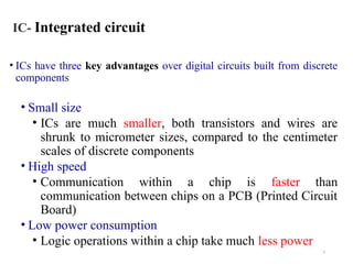
IC- Integrated circuit
•ICs have three key advantages over digital circuits built from discrete
components
• Small size
• ICs are much smaller, both transistors and wires are
shrunk to micrometer sizes, compared to the centimeter
scales of discrete components
• High speed
• Communication within a chip is faster than
communication between chips on a PCB (Printed Circuit
Board)
• Low power consumption
• Logic operations within a chip take much less power
6.
6
IC Packaging
Basic typesof IC packages
• The metal can or transistor pack: chip is encapsulated in a metal
or plastic case. Available with 3,5,8,10 or 12 pins
• LM117 (voltage regulator) has 3 pins
• Power op-amps, audio power amplifiers have 5 pins
• General purpose op-amps come in 8,10 or 12 pins
• The flat pack : the chip is enclosed in a rectangular ceramic case
with terminal leads extending through the sides and ends.
Comes with 8, 10, 14 or 16 pins
• The dual-in-line package (DIP): chip is mounted inside a plastic
or ceramic case
• Most widely used
• Available in 12, 14, 16 and 20 pins
7.
7
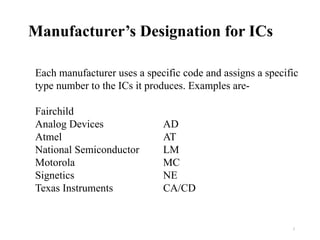
Manufacturer’s Designation forICs
Each manufacturer uses a specific code and assigns a specific
type number to the ICs it produces. Examples are-
Fairchild
Analog Devices AD
Atmel AT
National Semiconductor LM
Motorola MC
Signetics NE
Texas Instruments CA/CD
9
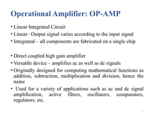
Operational Amplifier: OP-AMP
•Linear Integrated Circuit
• Linear– Output signal varies according to the input signal
• Integrated – all components are fabricated on a single chip
• Direct coupled high gain amplifier
• Versatile device – amplifies ac as well as dc signals
• Originally designed for computing mathematical functions as
addition, subtraction, multiplication and division, hence the
name
• Used for a variety of applications such as ac and dc signal
amplification, active filters, oscillators, comparators,
regulators, etc.
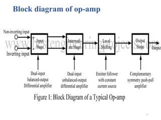
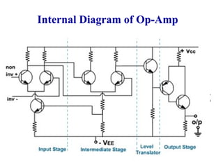
13
Stages of internalblock diagram
• Input Stage - The input stage is a Dual input balanced output
differential amplifier. The two amplifiers are applied at
inverting or non inverting terminals. This stage provides most
of voltage gain of the op-amp and decides input resistance
value R1.
• Intermediate Stage - It is driven by output of the input stage.
This stage is dual input unbalanced output differential amp.
This stage provides additional voltage gain to the input signals.
14.
14
Stages of internalblock diagram
• Level shifting stage - This is third stage in the block diagram of
op-amp. Due to direct coupling between first two stage the input of
level shifting stage is an amplifying system with non-zero DC level.
Level shifting stage is used to bring this DC level to a zero volt with
respect to ground.
• Output Stage - This is normally complementary output stage. It
increases magnitude of voltage and rises the current supplying
capacity of the op-amp. It also provides low output resistance. The
output stage is a push pull of two transistors.
16
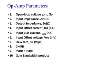
Op-Amp Parameters
• 1.Open-loop voltage gain, Go
• 2. Input impedance, Zin(Ω)
• 3. Output impedance, Zo(Ω)
• 4. Input Offset current, Ios (nA)
• 5. Input Bias current, IBIAS (nA)
• 6. Input Offset voltage, Vos (mV)
• 7. Slew rate, SR (V/μs)
• 8. CMRR
• 9. SVRR / PSRR
• 10 Gain Bandwidth product
17.
17
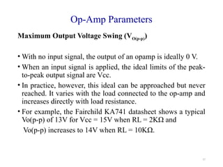
Op-Amp Parameters
Maximum OutputVoltage Swing (VO(p-p))
• With no input signal, the output of an opamp is ideally 0 V.
• When an input signal is applied, the ideal limits of the peak-
to-peak output signal are Vcc.
• In practice, however, this ideal can be approached but never
reached. It varies with the load connected to the op-amp and
increases directly with load resistance.
• For example, the Fairchild KA741 datasheet shows a typical
Vo(p-p) of 13V for Vcc = 15V when RL = 2KΩ and
Vo(p-p) increases to 14V when RL = 10KΩ.
18.
18
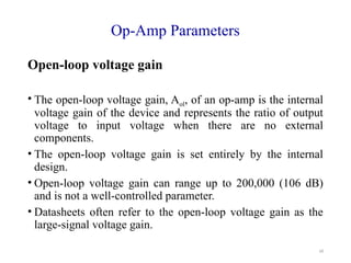
Op-Amp Parameters
Open-loop voltagegain
• The open-loop voltage gain, Aol, of an op-amp is the internal
voltage gain of the device and represents the ratio of output
voltage to input voltage when there are no external
components.
• The open-loop voltage gain is set entirely by the internal
design.
• Open-loop voltage gain can range up to 200,000 (106 dB)
and is not a well-controlled parameter.
• Datasheets often refer to the open-loop voltage gain as the
large-signal voltage gain.
19.
19
Op-Amp Parameters
Input offsetvoltage
• The ideal op-amp produces zero volts out for zero volts in.
• In a practical op-amp, however, a small dc voltage, VOUT(error),
appears at the output when no differential input voltage is
applied.
• Its primary cause is a slight mismatch of the base-emitter
voltages of the differential amplifier input stage of an op-amp.
• The input offset voltage, VOS, is the differential dc voltage
required between the inputs to force the output to zero volts.
• Typical values of input offset voltage are in the range of 2 mV
or less. In the ideal case, it is 0 V.
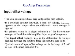
20.
20
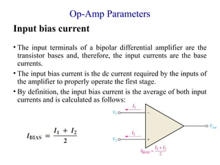
Op-Amp Parameters
Input biascurrent
• The input terminals of a bipolar differential amplifier are the
transistor bases and, therefore, the input currents are the base
currents.
• The input bias current is the dc current required by the inputs of
the amplifier to properly operate the first stage.
• By definition, the input bias current is the average of both input
currents and is calculated as follows:
21.
21
Op-Amp Parameters
Input offsetcurrent
• Ideally, the two input bias currents are equal, and thus their
difference is zero.
• In a practical op-amp, however, the bias currents are not exactly
equal.
• The input offset current, IOS, is the difference of the input bias
currents, expressed as an absolute value.
IOS = | I1 – I2 |
• Typical value is 200 nA
22.
22
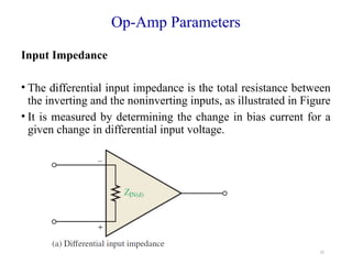
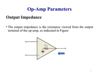
Op-Amp Parameters
Input Impedance
•The differential input impedance is the total resistance between
the inverting and the noninverting inputs, as illustrated in Figure
• It is measured by determining the change in bias current for a
given change in differential input voltage.
24
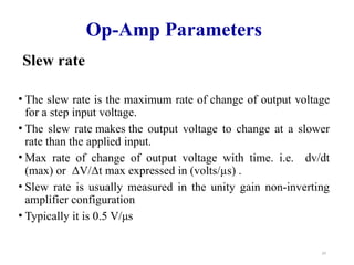
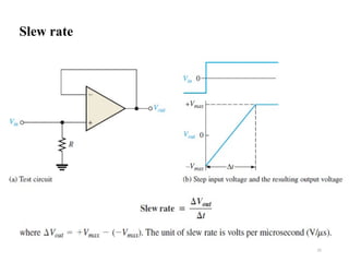
Op-Amp Parameters
Slew rate
•The slew rate is the maximum rate of change of output voltage
for a step input voltage.
• The slew rate makes the output voltage to change at a slower
rate than the applied input.
• Max rate of change of output voltage with time. i.e. dv/dt
(max) or ΔV/Δt max expressed in (volts/µs) .
• Slew rate is usually measured in the unity gain non-inverting
amplifier configuration
• Typically it is 0.5 V/μs
26
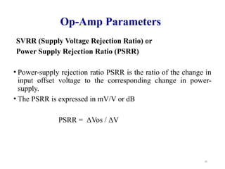
Op-Amp Parameters
SVRR (SupplyVoltage Rejection Ratio) or
Power Supply Rejection Ratio (PSRR)
• Power-supply rejection ratio PSRR is the ratio of the change in
input offset voltage to the corresponding change in power-
supply.
• The PSRR is expressed in mV/V or dB
PSRR = ΔVos / ΔV
27.
27
Op-Amp Parameters
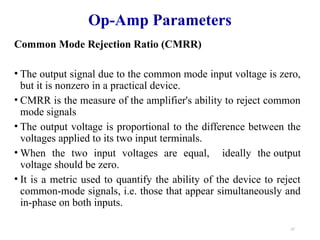
Common ModeRejection Ratio(CMRR)
• The output signal due to the common mode input voltage is zero,
but it is nonzero in a practical device.
• CMRR is the measure of the amplifier's ability to reject common
mode signals
• The output voltage is proportional to the difference between the
voltages applied to its two input terminals.
• When the two input voltages are equal, ideally the output
voltage should be zero.
• It is a metric used to quantify the ability of the device to reject
common-mode signals, i.e. those that appear simultaneously and
in-phase on both inputs.
28.
28
• A signalapplied to both input terminals of the op-amp is called
as common-mode signal. Usually it is an unwanted noise
voltage.
• CMRR is defined as the ratio of the open loop differential
voltage gain Aol to the common mode voltage gain Acm
CMRR = Aol / Acm
CMRR=20 log[Aol / Acm] dB
Common Mode Rejection Ratio(CMRR)
29.
29
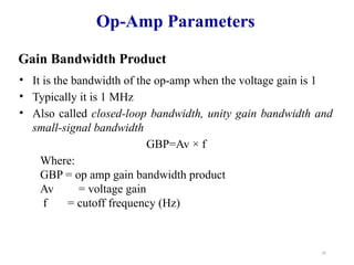
Op-Amp Parameters
Gain BandwidthProduct
• It is the bandwidth of the op-amp when the voltage gain is 1
• Typically it is 1 MHz
• Also called closed-loop bandwidth, unity gain bandwidth and
small-signal bandwidth
GBP=Av × f
Where:
GBP = op amp gain bandwidth product
Av = voltage gain
f = cutoff frequency (Hz)
30.
30
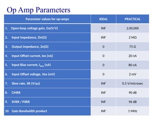
Op Amp Parameters
Parametervalues for op-amps IDEAL PRACTICAL
1. Open-loop voltage gain, Go(V/V) INF 2,00,000
2. Input impedance, Zin(Ω) INF 2 MΩ
3. Output impedance, Zo(Ω) 0 75 Ω
4. Input Offset current, Ios (nA) 0 20 nA
5. Input Bias current, IBIAS (nA) 0 80 nA
6. Input Offset voltage, Vos (mV) 0 2 mV
7. Slew rate, SR (V/μs) INF 0.5 V/microsec
8. CMRR INF 90 dB
9. SVRR / PSRR INF 96 dB
10 Gain Bandwidth product INF 1 MHz
31.
31
What is negativefeedback?
• Negative feedback is the most useful concepts in OPAMP
applications.
• It is the process whereby a portion of the output voltage of
an amplifier is returned to the input with a phase angle that
opposes the input signal.
32.
32
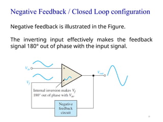
Negative Feedback /Closed Loop configuration
Negative feedback is illustrated in the Figure.
The inverting input effectively makes the feedback
signal 180° out of phase with the input signal.
33.
33
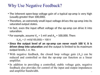
Why Use NegativeFeedback?
• The inherent open-loop voltage gain of a typical op-amp is very high
(usually greater than 100,000).
• Therefore, an extremely small input voltage drives the op-amp into its
saturated output states.
• In fact, even the input offset voltage of the op-amp can drive it into
saturation.
• For example, assume Vin = 1 mV and Aol = 100,000. Then:
VinAol = (1 mV)(100,000) = 100 V
• Since the output level of an op-amp can never reach 100 V, it is
driven deep into saturation and the output is limited to its maximum
output levels, i. e. Vcc.
• With negative feedback, the closed loop voltage gain (Acl) can be
reduced and controlled so that the op-amp can function as a linear
amplifier.
• In addition to providing a controlled, stable voltage gain, negative
feedback also provides for control of the input and output impedances
and amplifier bandwidth.
34.
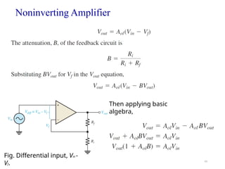
Closed-Loop Voltage Gain,Acl
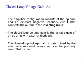
• The amplifier configuration consists of the op-amp
and an external negative feedback circuit that
connects the output to the inverting input.
• The closed-loop voltage gain is the voltage gain of
an op-amp with external feedback.
• The closed-loop voltage gain is determined by the
external component values and can be precisely
controlled by them.
34
35.
35
Virtual short andVirtual ground
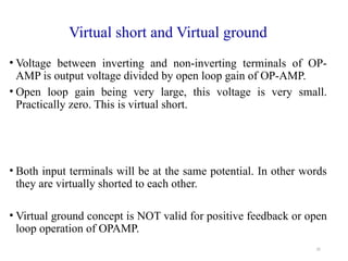
• Voltage between inverting and non-inverting terminals of OP-
AMP is output voltage divided by open loop gain of OP-AMP.
• Open loop gain being very large, this voltage is very small.
Practically zero. This is virtual short.
• Both input terminals will be at the same potential. In other words
they are virtually shorted to each other.
• Virtual ground concept is NOT valid for positive feedback or open
loop operation of OPAMP.
36.
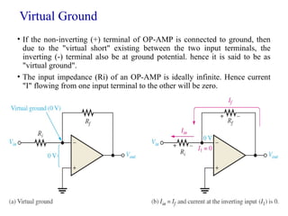
Virtual Ground
• Ifthe non-inverting (+) terminal of OP-AMP is connected to ground, then
due to the "virtual short" existing between the two input terminals, the
inverting (-) terminal also be at ground potential. hence it is said to be as
"virtual ground".
• The input impedance (Ri) of an OP-AMP is ideally infinite. Hence current
"I" flowing from one input terminal to the other will be zero.
36
37.
37
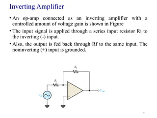
Inverting Amplifier
• Anop-amp connected as an inverting amplifier with a
controlled amount of voltage gain is shown in Figure
• The input signal is applied through a series input resistor Ri to
the inverting (-) input.
• Also, the output is fed back through Rf to the same input. The
noninverting (+) input is grounded.
38.
38
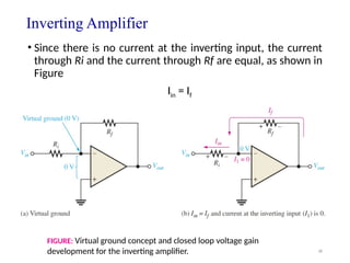
Inverting Amplifier
• Sincethere is no current at the inverting input, the current
through Ri and the current through Rf are equal, as shown in
Figure
Iin = If
FIGURE: Virtual ground concept and closed loop voltage gain
development for the inverting amplifier.
42
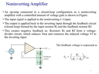
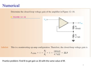
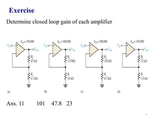
Noninverting Amplifier
• Anop-amp connected in a closed-loop configuration as a noninverting
amplifier with a controlled amount of voltage gain is shown in Figure.
• The input signal is applied to the noninverting (+) input.
• The output is applied back to the inverting input through the feedback circuit
(closed loop) formed by the input resistor Ri and the feedback resistor Rf.
• This creates negative feedback as: Resistors Ri and Rf form a voltage-
divider circuit, which reduces Vout and connects the reduced voltage Vf to
the inverting input.
The feedback voltage is expressed as
45
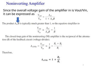
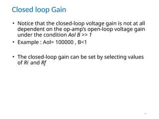
Closed loop Gain
•Notice that the closed-loop voltage gain is not at all
dependent on the op-amp’s open-loop voltage gain
under the condition Aol B >> 1
• Example : Aol= 100000 , B<1
• The closed-loop gain can be set by selecting values
of Ri and Rf
48
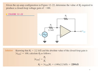
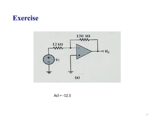
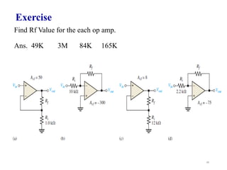
Find Rf Valuefor the each op amp.
Ans. 49K 3M 84K 165K
Exercise
49.
49
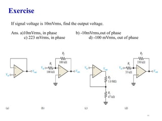
If signal voltageis 10mVrms, find the output voltage.
Ans. a)10mVrms, in phase b) -10mVrms,out of phase
c) 223 mVrms, in phase d) -100 mVrms, out of phase
Exercise
50.
50
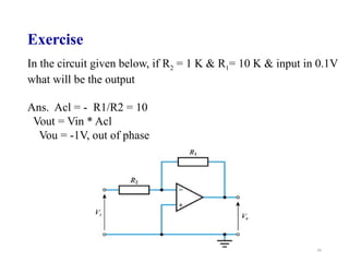
Exercise
In the circuitgiven below, if R2 = 1 K & R1= 10 K & input in 0.1V
what will be the output
Ans. Acl = - R1/R2 = 10
Vout = Vin * Acl
Vou = -1V, out of phase
52
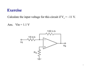
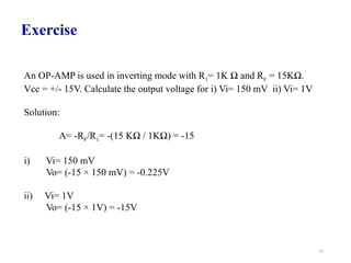
An OP-AMP isused in inverting mode with R1= 1K Ω and RF = 15KΩ.
Vcc = +/- 15V. Calculate the output voltage for i) Vi= 150 mV ii) Vi= 1V
Solution:
A= -RF/R1= -(15 KΩ / 1KΩ) = -15
i) Vi= 150 mV
Vo= (-15 × 150 mV) = -0.225V
ii) Vi= 1V
Vo= (-15 × 1V) = -15V
Exercise
53.
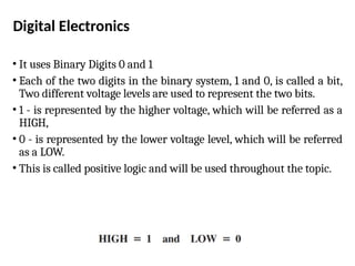
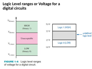
Digital Electronics
• Ituses Binary Digits 0 and 1
• Each of the two digits in the binary system, 1 and 0, is called a bit,
Two different voltage levels are used to represent the two bits.
• 1 - is represented by the higher voltage, which will be referred as a
HIGH,
• 0 - is represented by the lower voltage level, which will be referred
as a LOW.
• This is called positive logic and will be used throughout the topic.
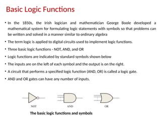
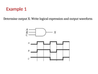
Basic Logic Functions
•In the 1850s, the Irish logician and mathematician George Boole developed a
mathematical system for formulating logic statements with symbols so that problems can
be written and solved in a manner similar to ordinary algebra
• The term logic is applied to digital circuits used to implement logic functions.
• Three basic logic functions - NOT, AND, and OR
• Logic functions are indicated by standard symbols shown below
• The inputs are on the left of each symbol and the output is on the right.
• A circuit that performs a specified logic function (AND, OR) is called a logic gate.
• AND and OR gates can have any number of inputs.
The basic logic functions and symbols
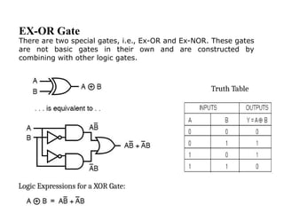
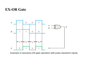
EX-OR Gate
Logic Expressionsfor a XOR Gate:
Truth Table
There are two special gates, i.e., Ex-OR and Ex-NOR. These gates
are not basic gates in their own and are constructed by
combining with other logic gates.
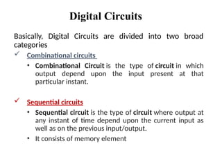
Digital Circuits
Basically, DigitalCircuits are divided into two broad
categories
Combinational circuits
• Combinational Circuit is the type of circuit in which
output depend upon the input present at that
particular instant.
Sequential circuits
• Sequential circuit is the type of circuit where output at
any instant of time depend upon the current input as
well as on the previous input/output.
• It consists of memory element
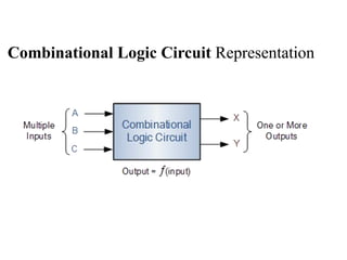
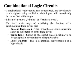
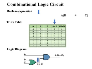
Combinational Logic Circuits
•Combinational logic circuits have no feedback, and any changes
to the signals being applied to their inputs will immediately
have an effect at the output.
• It has no “memory”, “timing” or “feedback loops”.
• The three main ways of specifying the function of a
combinational logic circuit are:
• Boolean Expression – This forms the algebraic expression
showing the operation of the logic circuit
• Truth Table – Shows all the output states in tabular form
for each possible combination of input variable
• Logic Diagram – This is a graphical representation of a
logic circuit
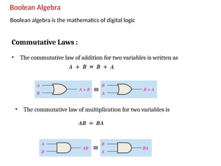
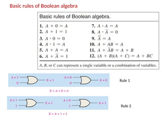
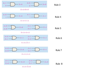
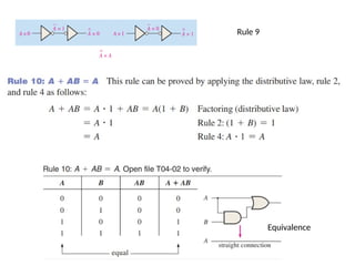
Boolean Algebra
Boolean algebrais the mathematics of digital logic
Commutative Laws :
• The commutative law of addition for two variables is written as
• The commutative law of multiplication for two variables is
67.
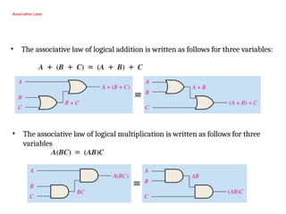
Associative Laws
• Theassociative law of logical addition is written as follows for three variables:
• The associative law of logical multiplication is written as follows for three
variables
68.
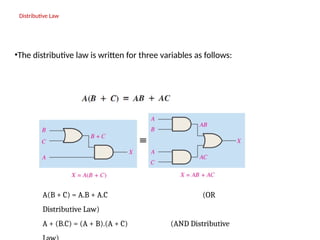
Distributive Law
•The distributivelaw is written for three variables as follows:
A(B + C) = A.B + A.C (OR
Distributive Law)
A + (B.C) = (A + B).(A + C) (AND Distributive
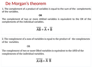
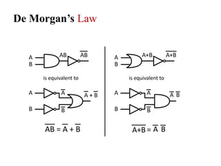
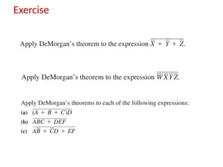
De Morgan’s theorem
1.The complement of a product of variables is equal to the sum of the complements
of the variables.
OR
The complement of two or more ANDed variables is equivalent to the OR of the
complements of the individual variables.
2. The complement of a sum of variables is equal to the product of the complements
of the variables.
OR
The complement of two or more ORed variables is equivalent to the AND of the
complements of the individual variables.
75.
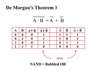
De Morgan’s Theorem1
A B A B A B A B A + B
0 0 0 1 1 1 1
0 1 0 1 1 0 1
1 0 0 1 0 1 1
1 1 1 0 0 0 0
A · B = A + B
EQUAL
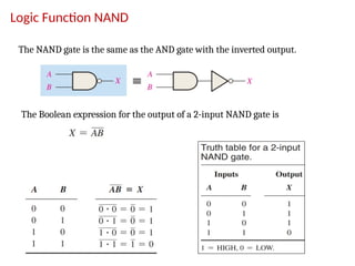
NAND = Bubbled OR
76.
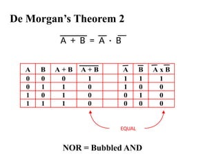
De Morgan’s Theorem2
A + B = A · B
A B A + B A + B A B A x B
0 0 0 1 1 1 1
0 1 1 0 1 0 0
1 0 1 0 0 1 0
1 1 1 0 0 0 0
EQUAL
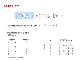
NOR = Bubbled AND
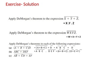
Exercise- Solution
= X.Y . Z
= W + X + Y + Z
= ( A + B + C ) + D = A B C + D
= A B C . D E F = (A + B + C) . ( D + E + F )
82.
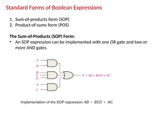
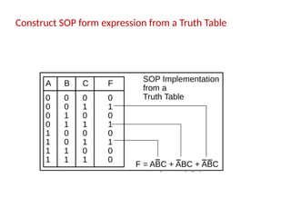
Standard Forms ofBoolean Expressions
1. Sum-of-products form (SOP)
2. Product-of-sums form (POS)
The Sum-of-Products (SOP) Form:
• An SOP expression can be implemented with one OR gate and two or
more AND gates.
83.
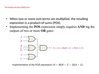
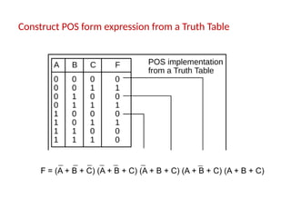
The Product-of-Sums (POS)Form
• When two or more sum terms are multiplied, the resulting
expression is a product-of-sums (POS).
• Implementing the POS expression simply requires AND ing the
outputs of two or more OR gates
Construct POS formexpression from a Truth Table
F = (A + B + C) (A + B + C) (A + B + C) (A + B + C) (A + B + C)
86.
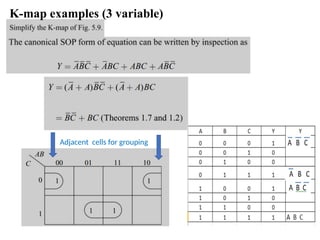
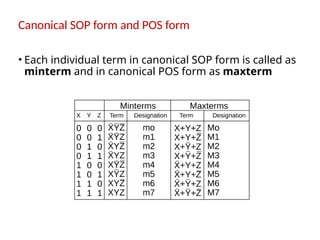
Canonical SOP formand POS form
• Each individual term in canonical SOP form is called as
minterm and in canonical POS form as maxterm
87.
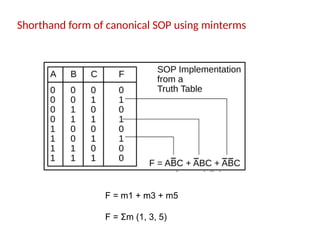
Shorthand form ofcanonical SOP using minterms
F = m1 + m3 + m5
F = Σm (1, 3, 5)
88.
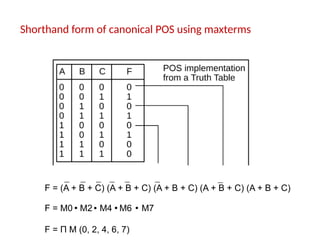
Shorthand form ofcanonical POS using maxterms
F = (A + B + C) (A + B + C) (A + B + C) (A + B + C) (A + B + C)
F = M0 M2 M4 M6 M7
F = Π M (0, 2, 4, 6, 7)
89.
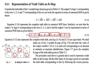
Simplification of Booleanexpression
• The required Boolean results are transferred from a
truth table onto a two-dimensional grid where, in Karnaugh
maps, the cells are ordered in Gray code,[6][4]
and each cell
position represents one combination of input conditions,
while each cell value represents the corresponding output
value. Optimal groups of 1s or 0s are identified, which
represent the terms of a canonical form of the logic in the
original truth table.[7]
These terms can be used to write a
minimal Boolean expression representing the required logic.
90.
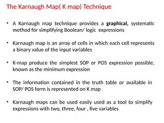
The Karnaugh Map(K map) Technique
• A Karnaugh map technique provides a graphical, systematic
method for simplifying Boolean/ logic expressions
• Karnaugh map is an array of cells in which each cell represents
a binary value of the input variables
• K-map produce the simplest SOP or POS expression possible,
known as the minimum expression
• The information contained in the truth table or available in
SOP/ POS form is represented on K map
• Karnaugh maps can be used easily used as a tool to simplify
expressions with two, three, four , five variables
91.
K-maps
• K-maps adjacencieswrap around
edges
• Wrap from first to last column
• Wrap top row to bottom row
• Numbering scheme is based on
Gray–code (only a single bit
changes in code for adjacent map
cells
• K-maps are hard to draw and
visualize for more than 4
dimensions, and
virtually impossible for more than
6 dimensions
92.
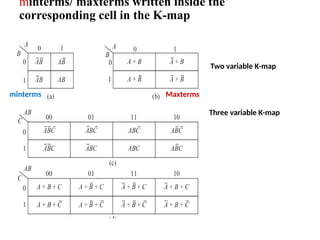
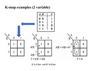
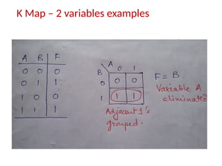
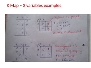
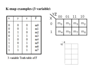
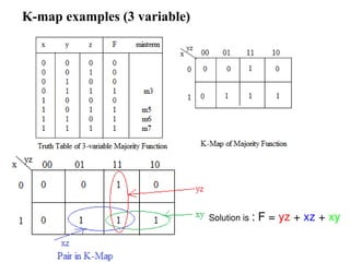
Two variable K-map
Threevariable K-map
minterms/ maxterms written inside the
corresponding cell in the K-map
minterms Maxterms
93.
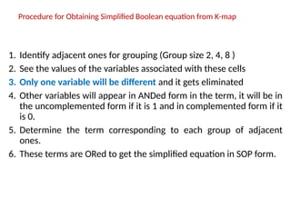
Procedure for ObtainingSimplified Boolean equation from K-map
1. Identify adjacent ones for grouping (Group size 2, 4, 8 )
2. See the values of the variables associated with these cells
3. Only one variable will be different and it gets eliminated
4. Other variables will appear in ANDed form in the term, it will be in
the uncomplemented form if it is 1 and in complemented form if it
is 0.
5. Determine the term corresponding to each group of adjacent
ones.
6. These terms are ORed to get the simplified equation in SOP form.
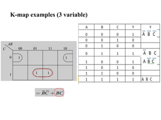
Solution is :F = yz + xz + xy
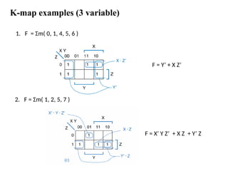
K-map examples (3 variable)
100.
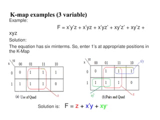
Example:
F = x’y’z+ x’yz + x’yz’ + xy’z’ + xy’z +
xyz
Solution:
The equation has six minterms. So, enter 1’s at appropriate positions in
the K-Map
Solution is: F = z + x’y + xy’
K-map examples (3 variable)
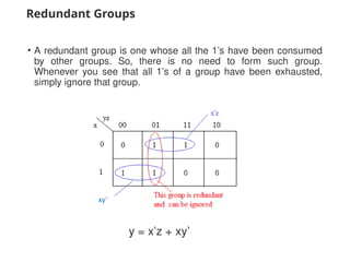
Redundant Groups
• Aredundant group is one whose all the 1’s have been consumed
by other groups. So, there is no need to form such group.
Whenever you see that all 1’s of a group have been exhausted,
simply ignore that group.
y = x’z + xy’
xy’
104.
K-map examples (3variable)
1. F = Σm( 0, 1, 4, 5, 6 )
F = Y’ + X Z’
2. F = Σm( 1, 2, 5, 7 )
F = X’ Y Z’ + X Z + Y’ Z
105.
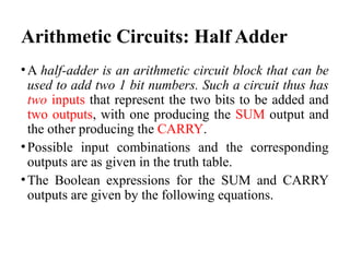
Arithmetic Circuits: HalfAdder
•A half-adder is an arithmetic circuit block that can be
used to add two 1 bit numbers. Such a circuit thus has
two inputs that represent the two bits to be added and
two outputs, with one producing the SUM output and
the other producing the CARRY.
•Possible input combinations and the corresponding
outputs are as given in the truth table.
•The Boolean expressions for the SUM and CARRY
outputs are given by the following equations.
106.
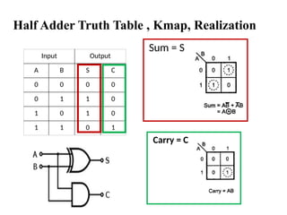
Half Adder TruthTable , Kmap, Realization
Input Output
A B S C
0 0 0 0
0 1 1 0
1 0 1 0
1 1 0 1
Sum = S
Carry = C
107.
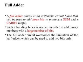
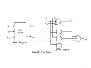
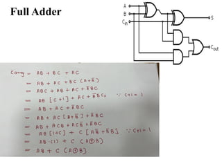
Full Adder
•A fulladder circuit is an arithmetic circuit block that
can be used to add three bits to produce a SUM and a
CARRY output.
•Such a building block is needed in order to add binary
numbers with a large number of bits.
•The full adder circuit overcomes the limitation of the
half-adder, which can be used to add two bits only
108.
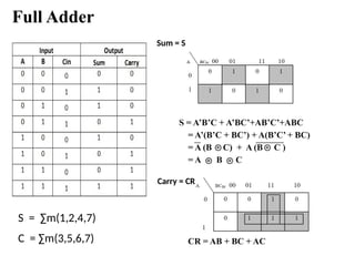
Full Adder
Sum =S
Carry = CR
S = A’B’C + A’BC’+AB’C’+ABC
= A’(B’C + BC’) + A(B’C’ + BC)
= A (B C) + A (B C )
= A B C
CR = AB + BC + AC
S = ∑m(1,2,4,7)
C = ∑m(3,5,6,7)
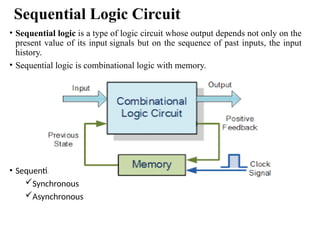
Sequential Logic Circuit
•Sequential logic is a type of logic circuit whose output depends not only on the
present value of its input signals but on the sequence of past inputs, the input
history.
• Sequential logic is combinational logic with memory.
• Sequential logic circuits are classified in 2 categories
Synchronous
Asynchronous
112.
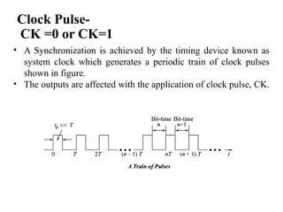
Clock Pulse-
CK =0or CK=1
• A Synchronization is achieved by the timing device known as
system clock which generates a periodic train of clock pulses
shown in figure.
• The outputs are affected with the application of clock pulse, CK.
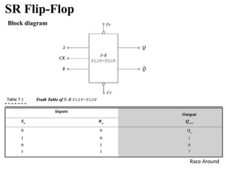
SR Flip flopOperation
S.N. Condition Operation
1 S = R = 0 , CK=1 If S = R = 0 then output of NAND gates 3 and 4 are
forced to become 1.
Hence R' and S' both will be equal to 1. Since S' and R'
are the input of the basic S-R latch using NAND gates,
there will be no change in the state of outputs.
2 S = 0, R = 1, CK = 1 Since S = 0, output of NAND-3 i.e. R' = 1 and CK = 1 the
output of NAND-4 i.e. S' = 0.
Hence Qn+1 = 0 and Qn+1 bar = 1. This is reset condition.
3 S = 1, R = 0, CK = 1 Output of NAND-3 i.e. R' = 0 and output of NAND-4 i.e.
S' = 1.
Hence output of S-R NAND latch is Qn+1 = 1 and Qn+1 bar =
0. This is the set condition.
4 S = 1, R = 1, CK = 1 As S = 1, R = 1 and E = 1, the output of NAND gates 3 and
4 both are 0 i.e. S' = R' = 0.
Hence the Race condition will occur in the basic NAND
latch.
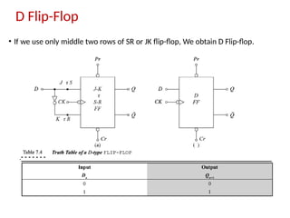
D Flip-Flop
• Ifwe use only middle two rows of SR or JK flip-flop, We obtain D Flip-flop.
118.
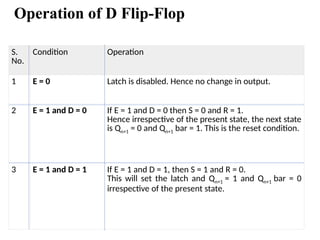
Operation of DFlip-Flop
S.
No.
Condition Operation
1 E = 0 Latch is disabled. Hence no change in output.
2 E = 1 and D = 0 If E = 1 and D = 0 then S = 0 and R = 1.
Hence irrespective of the present state, the next state
is Qn+1 = 0 and Qn+1 bar = 1. This is the reset condition.
3 E = 1 and D = 1 If E = 1 and D = 1, then S = 1 and R = 0.
This will set the latch and Qn+1 = 1 and Qn+1 bar = 0
irrespective of the present state.
119.
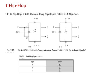
T Flip-Flop
• InJK flip-flop, if J=K, the resulting Flip-flop is called as T Flip-flop.
120.
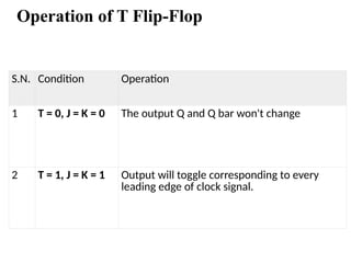
Operation of TFlip-Flop
S.N. Condition Operation
1 T = 0, J = K = 0 The output Q and Q bar won't change
2 T = 1, J = K = 1 Output will toggle corresponding to every
leading edge of clock signal.
121.
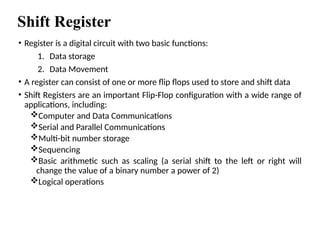
Shift Register
• Registeris a digital circuit with two basic functions:
1. Data storage
2. Data Movement
• A register can consist of one or more flip flops used to store and shift data
• Shift Registers are an important Flip-Flop configuration with a wide range of
applications, including:
Computer and Data Communications
Serial and Parallel Communications
Multi-bit number storage
Sequencing
Basic arithmetic such as scaling (a serial shift to the left or right will
change the value of a binary number a power of 2)
Logical operations
122.
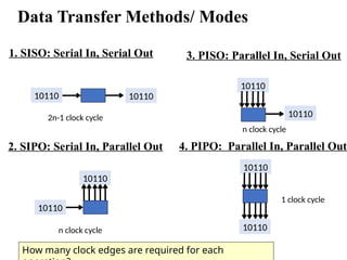
Data Transfer Methods/Modes
1. SISO: Serial In, Serial Out
How many clock edges are required for each
10110 10110
10110
10110
10110
10110
10110
10110
2. SIPO: Serial In, Parallel Out
3. PISO: Parallel In, Serial Out
4. PIPO: Parallel In, Parallel Out
2n-1 clock cycle
n clock cycle
n clock cycle
1 clock cycle
123.
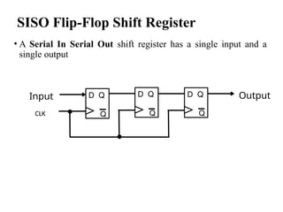
SISO Flip-Flop ShiftRegister
• A Serial In Serial Out shift register has a single input and a
single output
D Q
Q
D Q
Q
D Q
Q
Input Output
CLK
124.
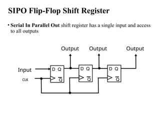
SIPO Flip-Flop ShiftRegister
• Serial In Parallel Out shift register has a single input and access
to all outputs
D Q
Q
D Q
Q
D Q
Q
Input
Output Output Output
CLK
125.
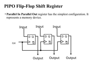
PIPO Flip-Flop ShiftRegister
• Parallel In Parallel Out register has the simplest configuration. It
represents a memory device.
D Q
Q
Input
Output
D Q
Q
Output
D Q
Q
Output
Input Input
CLK
126.
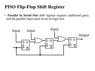
PISO Flip-Flop ShiftRegister
• Parallel In Serial Out shift register requires additional gates,
and the parallel input must revert to logic low.
Input
D Q
1
Q
Input
Output
Input
D Q
0
Q
D Q
0
Q


![28
• A signal applied to both input terminals of the op-amp is called
as common-mode signal. Usually it is an unwanted noise
voltage.
• CMRR is defined as the ratio of the open loop differential
voltage gain Aol to the common mode voltage gain Acm
CMRR = Aol / Acm
CMRR=20 log[Aol / Acm] dB
Common Mode Rejection Ratio(CMRR)](https://image.slidesharecdn.com/ic-250830045820-92de7f56/85/IC-Integrated-circuits-ppt-for-undergraduate-course-pptx-28-320.jpg)
![Simplification of Boolean expression
• The required Boolean results are transferred from a
truth table onto a two-dimensional grid where, in Karnaugh
maps, the cells are ordered in Gray code,[6][4]
and each cell
position represents one combination of input conditions,
while each cell value represents the corresponding output
value. Optimal groups of 1s or 0s are identified, which
represent the terms of a canonical form of the logic in the
original truth table.[7]
These terms can be used to write a
minimal Boolean expression representing the required logic.](https://image.slidesharecdn.com/ic-250830045820-92de7f56/85/IC-Integrated-circuits-ppt-for-undergraduate-course-pptx-89-320.jpg)