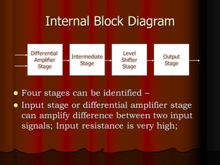
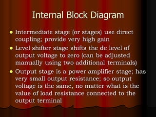
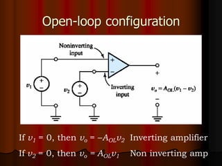
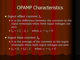
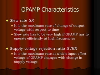
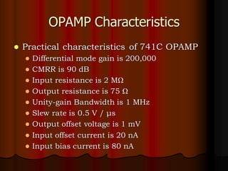
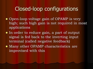
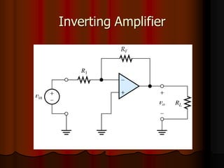
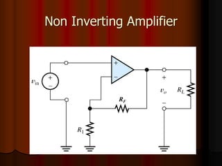
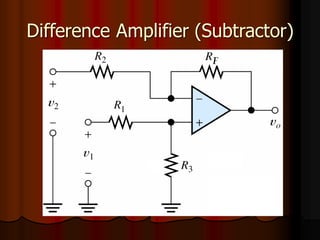
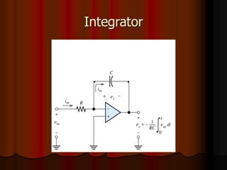
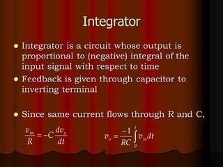
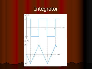
Module 4
Operational Amplifier
Prepared by
KMN
Contents
⚫ Introduction
⚫ OPAMP Symbol
⚫ Internal block diagram
⚫ Open-loop configuration
⚫ Common mode rejection ratio
⚫ OPAMP equivalent circuit
⚫ OPAMP characteristics
⚫ Closed-loop configuration
Contents
⚫ Inverting Amplifier
⚫ Non-inverting Amplifier
⚫ Summing Amplifier Difference Amplifier
⚫ Differentiator
⚫ Integrator
⚫ Tutorials
Reference book
⚫ OPAMPS and Linear Integrated Circuits
by Ramakanth Gayakwad
Introduction
⚫ Operational Amplifier (OPAMP) is a very
high gain amplifier fabricated on Integrated
Circuit (IC)
⚫ Finds application in
⚫ Audio amplifier
⚫ Signal generator
⚫ Signal filters
⚫ Biomedical Instrumentation
⚫ And numerous other applications
Introduction
⚫ Advantages of OPAMP over transistor
amplifier
⚫ Less power consumption
⚫ Costs less
⚫ More compact
⚫ More reliable
⚫ Higher gain can be obtained
⚫ Easy design
OPAMP terminals
+VC
C
+
–
Non inverting
input
Inverting input
Output
–VEE
OPAMP terminals
OPAMP terminals
⚫ If input is applied to non inverting input
terminal, then output will be in-phase with
input
⚫ If input is applied to inverting input
terminal, then output will be 180 degrees
out of phase with input
⚫ If inputs are applied to both terminals, then
output will be proportional to difference
between the two inputs
OPAMP terminals
⚫ Two DC power supplies (dual) are required
⚫ Magnitudes of both may be same
⚫ The other terminal of both power supplies
are connected to common ground
⚫ All input and output voltages are measured
with reference to the common ground
OPAMP terminals
Integrated Circuit
Internal Block Diagram
⚫ Four stages can be identified –
⚫ Input stage or differential amplifier stage
can amplify difference between two input
signals; Input resistance is very high;
Intermediate
Stage
Level
Shifter
Stage
Output
Stage
Differential
Amplifier
Stage
Internal Block Diagram
⚫ Intermediate stage (or stages) use direct
coupling; provide very high gain
⚫ Level shifter stage shifts the dc level of
output voltage to zero (can be adjusted
manually using two additional terminals)
⚫ Output stage is a power amplifier stage; has
very small output resistance; so output
voltage is the same, no matter what is the
value of load resistance connected to the
output terminal
Open-loop configuration
If v1 = 0, then vo = –AOLv2 Inverting amplifier
If v2 = 0, then vo = AOLv1 Non inverting amp
Open-loop configuration
⚫ AOL is the open-loop voltage gain of OPAMP
Its value is very high
Typical value is 0.5 million
⚫ So, even if input is in micro volts, output
will be in volts
⚫ But output voltage cannot cross the value
of power supply VCC
⚫ So, if input is in milli volts, output reaches
saturation value Vsat = VCC (or VEE)
Open-loop configuration
⚫ If v1 = v2, then ideally output should be zero
⚫ But in practical Op-Amp, output is
Where, ACM is the common-mode gain of
Op-Amp
⚫ So, final gain equation is:





 +
=
2
v
v
A
v 2
1
cm
o
( ) 




 +
+
−
=
2
v
v
A
v
v
A
v 2
1
cm
2
1
d
o
icm
cm
id
d
o v
A
v
A
v +
=
Open-loop configuration
⚫ Common-mode rejection ratio
⚫ It is a measure of the ability of Op-Amp
to reject the signals common to both
input terminals (noise)
⚫ Defined as
cm
d
A
A
CMRR =
( ) 







=
cm
d
10
dB
A
A
log
20
CMRR
Problems
⚫ An OPAMP has differential voltage gain of 100,000
and CMRR of 60 dB. If non inverting input voltage
is 150 μV and inverting input voltage is 140 μV,
calculate the output voltage of OPAMP
Ans: 1.01 V
⚫ For an OPAMP, when v1 is 0.5 mV and v2 is –0.5
mV, output voltage is 8 V. For the same OPAMP,
when v1 = v2 = 1 mV, output voltage is 12 mV.
Calculate the CMRR of the OPAMP
Ans: 56.48 dB
OPAMP equivalent circuit
+
–
vo
vi2
vi1
Ri
AOLvid
Ro
Practical OPAMP
OPAMP equivalent circuit
Ideal OPAMP
+
–
vo
vi2
vi1
AOLvid
OPAMP Characteristics
⚫ Ideal OPAMP
⚫ Infinite differential mode gain
⚫ Zero common mode gain
⚫ Infinite CMRR
⚫ Infinite input resistance
⚫ Zero output resistance
⚫ Infinite bandwidth
⚫ Infinite slew rate
⚫ Zero input offset voltage
⚫ Zero input offset current
⚫ Zero output offset voltage
OPAMP Characteristics
⚫ Differential mode gain Ad
⚫ It is the factor by which the difference between
the two input signals is amplified by the OPAMP
⚫ Common mode gain Acm
⚫ It is the factor by which the common mode input
voltage is amplified by the OPAMP
⚫ Common mode rejection ratio CMRR
⚫ Is the ratio of Ad to Acm expressed in decibels
OPAMP Characteristics
⚫ Input resistance Ri
⚫ It is the equivalent resistance measured between
the two input terminals of OPAMP
⚫ Output resistance Ro
⚫ It is equivalent resistance measured between
output terminal and ground
⚫ Bandwidth
⚫ It is the range of frequency over which the gain
of OPAMP is almost constant
OPAMP Characteristics
⚫ Output offset voltage Voo
⚫ It is the output voltage when both input voltages
are zero
⚫ Denoted as Voo
⚫ Input offset voltage Vio
⚫ It is the differential input voltage that must be
applied at the input terminals in order to make
output voltage equal to zero
⚫ Vio = |v1 – v2| for vo = 0
OPAMP Characteristics
⚫ Input offset current Iio
⚫ It is the difference between the currents in the
input terminals when both input voltages are
zero
⚫ Iio = | I1 – I2 | when v1 = v2 = 0
⚫ Input bias current Iib
⚫ It is the average of the currents in the input
terminals when both input voltages are zero
⚫ Iib = (I1 + I2) / 2 when v1 = v2 = 0
OPAMP Characteristics
⚫ Slew rate SR
⚫ It is the maximum rate of change of output
voltage with respect to time
⚫ Slew rate has to be very high if OPAMP has to
operate efficiently at high frequencies
⚫ Supply voltage rejection ratio SVRR
⚫ It is the maximum rate at which input offset
voltage of OPAMP changes with change in
supply voltage
OPAMP Characteristics
⚫ Practical characteristics of 741C OPAMP
⚫ Differential mode gain is 200,000
⚫ CMRR is 90 dB
⚫ Input resistance is 2 MΩ
⚫ Output resistance is 75 Ω
⚫ Unity-gain Bandwidth is 1 MHz
⚫ Slew rate is 0.5 V / μs
⚫ Output offset voltage is 1 mV
⚫ Input offset current is 20 nA
⚫ Input bias current is 80 nA
Closed-loop configurations
⚫ Open-loop voltage gain of OPAMP is very
high; such high gain is not required in most
applications
⚫ In order to reduce gain, a part of output
signal is fed back to the inverting input
terminal (called negative feedback)
⚫ Many other OPAMP characteristics are
improvised with this
Inverting Amplifier
RF
Inverting Amplifier
⚫ Input is applied to inverting terminal
⚫ Non inverting is grounded
⚫ Feedback is given to inverting terminal
through resistor RF
⚫ Assuming vo is less than VCC
since Ad is very high, vid should be very
small; vid taken as almost zero
⚫ Current entering OPAMP input terminal is
almost zero
Inverting Amplifier
RF
Virtual
ground
+
0 V
–
0
i1
i2
Inverting Amplifier
1
1
1
0
R
v
R
v
i in
in
=
−
=
F
o
F
o
R
v
R
v
i
−
=
−
=
0
2
2
1 i
i =
F
o
in
R
v
R
v −
=
1
1
R
R
v
v F
in
o −
=
1
R
R
v
v
A F
in
o
V −
=
=
Non Inverting Amplifier
RF
Non Inverting Amplifier
⚫ Input is applied to non inverting terminal
⚫ Feedback is given to inverting terminal
⚫ Output voltage will be in-phase with input
voltage
⚫ Here again, the following assumptions are
made
⚫ Since Ad is very high, vid should be very small;
vid taken as almost zero
⚫ Current entering OPAMP input terminal is
almost zero
Non Inverting Amplifier
RF
v1
v2
i2
i1
Non Inverting Amplifier
0
=
id
v in
v
v
v =
= 2
1
1
1
2
1
R
v
R
v
i in
=
=
F
in
o
F
o
R
v
v
R
v
v
i
−
=
−
= 2
2
2
1 i
i =
F
in
o
in
R
v
v
R
v −
=
1








+
=
1
1
R
R
v
v F
in
o
Problems
⚫ For an inverting amplifier using OPAMP, R1=1K,
RF=100K, vin=0.1sin(ωt). Find vo.
Ans: –10sin(ωt)
⚫ For a non inverting amplifier, R1=10K, RF=100K.
Calculate vo if vi = 25 mV dc.
Ans: 275 mV dc
⚫ An ac signal of rms value 2 mV needs to be
amplified to 1.024 V rms, 180 degree phase shifted.
Design a suitable amplifier choosing R1=1.2K
Ans: Inv amplifier with RF=614.4K
Voltage Follower
⚫ Special case of non inverting amplifier where RF=0
⚫ Voltage gain is unity. vo = vin
⚫ Has very high input resistance and very low output
resistance; Used as buffer for impedance matching
Summing Amplifier (Adder)
iA
iB
iF
Summing Amplifier (Adder)
⚫ If RA=RB=RF, then
A
A
A
R
v
i =
B
B
B
R
v
i =
F
B
A i
i
i =
+
F
o
F
R
v
i
−
=
F
o
B
B
A
A
R
v
R
v
R
v
−
=
+








+
−
=
B
F
B
A
F
A
o
R
R
v
R
R
v
v
( )
B
A
o v
v
v +
−
=
Difference Amplifier (Subtractor)
⚫ The circuit is analyzed using superposition
theorem
⚫ Consider only v1 to be present; v2=0
Now derive expression for output voltage vo1
⚫ Next consider only v2 to be present; v1=0
Derive expression for output voltage v02
⚫ Actual output voltage vo = vo1+vo2
Difference Amplifier (Subtractor)
vx








+
=
2
1
1
R
R
v
v F
x
o 







+








+
=
2
3
1
3
1
1
1
R
R
R
R
R
v
v F
o
Difference Amplifier (Subtractor)
2
2
2
R
R
v
v F
o −
=
2
2
2
3
1
3
1
2
1
1
R
R
v
R
R
R
R
R
v
v
v
v F
F
o
o
o −








+








+
=
+
=
F
R
3
R
2
R
1
R
if
2
1 =
=
=
−
= v
v
Problems
⚫ Design an OPAMP circuit such that output is
given by vo=–(0.5v1+0.75v2) where v1 and v2 are
input voltages. Choose RF=10K
⚫ Design an OPAMP subtractor to have output
given by Choose RF=R2=1K
⚫ Design an OPAMP adder/subtractor to get
output voltage
2
1
3
2
o v
v
v −
=
3
2
3
2
1
2
1
o v
v
v
v −
+
−
=
Integrator
Integrator
⚫ Integrator is a circuit whose output is
proportional to (negative) integral of the
input signal with respect to time
⚫ Feedback is given through capacitor to
inverting terminal
⚫ Since same current flows through R and C,
dt
dv
C
R
v o
in
−
= 
−
=
t
0
in
o dt
v
v
RC
1
Integrator
Differentiator
Differentiator
⚫ Differentiator is circuit whose output is
proportional to (negative) differential of
input voltage with respect to time
⚫ Input is given through capacitor, feedback
given through resistor to inv terminal
⚫ Since current through R and C are same,
R
v
dt
dv
C o
in
−
=
dt
dv
v in
o RC
−
=
End of Module 4

Basic engineering electronics Op Amp.pdf

  • 1.
  • 2.
    Contents ⚫ Introduction ⚫ OPAMPSymbol ⚫ Internal block diagram ⚫ Open-loop configuration ⚫ Common mode rejection ratio ⚫ OPAMP equivalent circuit ⚫ OPAMP characteristics ⚫ Closed-loop configuration
  • 3.
    Contents ⚫ Inverting Amplifier ⚫Non-inverting Amplifier ⚫ Summing Amplifier Difference Amplifier ⚫ Differentiator ⚫ Integrator ⚫ Tutorials
  • 4.
    Reference book ⚫ OPAMPSand Linear Integrated Circuits by Ramakanth Gayakwad
  • 5.
    Introduction ⚫ Operational Amplifier(OPAMP) is a very high gain amplifier fabricated on Integrated Circuit (IC) ⚫ Finds application in ⚫ Audio amplifier ⚫ Signal generator ⚫ Signal filters ⚫ Biomedical Instrumentation ⚫ And numerous other applications
  • 6.
    Introduction ⚫ Advantages ofOPAMP over transistor amplifier ⚫ Less power consumption ⚫ Costs less ⚫ More compact ⚫ More reliable ⚫ Higher gain can be obtained ⚫ Easy design
  • 7.
  • 8.
  • 9.
    OPAMP terminals ⚫ Ifinput is applied to non inverting input terminal, then output will be in-phase with input ⚫ If input is applied to inverting input terminal, then output will be 180 degrees out of phase with input ⚫ If inputs are applied to both terminals, then output will be proportional to difference between the two inputs
  • 10.
    OPAMP terminals ⚫ TwoDC power supplies (dual) are required ⚫ Magnitudes of both may be same ⚫ The other terminal of both power supplies are connected to common ground ⚫ All input and output voltages are measured with reference to the common ground
  • 11.
  • 12.
    Internal Block Diagram ⚫Four stages can be identified – ⚫ Input stage or differential amplifier stage can amplify difference between two input signals; Input resistance is very high; Intermediate Stage Level Shifter Stage Output Stage Differential Amplifier Stage
  • 13.
    Internal Block Diagram ⚫Intermediate stage (or stages) use direct coupling; provide very high gain ⚫ Level shifter stage shifts the dc level of output voltage to zero (can be adjusted manually using two additional terminals) ⚫ Output stage is a power amplifier stage; has very small output resistance; so output voltage is the same, no matter what is the value of load resistance connected to the output terminal
  • 14.
    Open-loop configuration If v1= 0, then vo = –AOLv2 Inverting amplifier If v2 = 0, then vo = AOLv1 Non inverting amp
  • 15.
    Open-loop configuration ⚫ AOLis the open-loop voltage gain of OPAMP Its value is very high Typical value is 0.5 million ⚫ So, even if input is in micro volts, output will be in volts ⚫ But output voltage cannot cross the value of power supply VCC ⚫ So, if input is in milli volts, output reaches saturation value Vsat = VCC (or VEE)
  • 16.
    Open-loop configuration ⚫ Ifv1 = v2, then ideally output should be zero ⚫ But in practical Op-Amp, output is Where, ACM is the common-mode gain of Op-Amp ⚫ So, final gain equation is:       + = 2 v v A v 2 1 cm o ( )       + + − = 2 v v A v v A v 2 1 cm 2 1 d o icm cm id d o v A v A v + =
  • 17.
    Open-loop configuration ⚫ Common-moderejection ratio ⚫ It is a measure of the ability of Op-Amp to reject the signals common to both input terminals (noise) ⚫ Defined as cm d A A CMRR = ( )         = cm d 10 dB A A log 20 CMRR
  • 18.
    Problems ⚫ An OPAMPhas differential voltage gain of 100,000 and CMRR of 60 dB. If non inverting input voltage is 150 μV and inverting input voltage is 140 μV, calculate the output voltage of OPAMP Ans: 1.01 V ⚫ For an OPAMP, when v1 is 0.5 mV and v2 is –0.5 mV, output voltage is 8 V. For the same OPAMP, when v1 = v2 = 1 mV, output voltage is 12 mV. Calculate the CMRR of the OPAMP Ans: 56.48 dB
  • 19.
  • 20.
    OPAMP equivalent circuit IdealOPAMP + – vo vi2 vi1 AOLvid
  • 21.
    OPAMP Characteristics ⚫ IdealOPAMP ⚫ Infinite differential mode gain ⚫ Zero common mode gain ⚫ Infinite CMRR ⚫ Infinite input resistance ⚫ Zero output resistance ⚫ Infinite bandwidth ⚫ Infinite slew rate ⚫ Zero input offset voltage ⚫ Zero input offset current ⚫ Zero output offset voltage
  • 22.
    OPAMP Characteristics ⚫ Differentialmode gain Ad ⚫ It is the factor by which the difference between the two input signals is amplified by the OPAMP ⚫ Common mode gain Acm ⚫ It is the factor by which the common mode input voltage is amplified by the OPAMP ⚫ Common mode rejection ratio CMRR ⚫ Is the ratio of Ad to Acm expressed in decibels
  • 23.
    OPAMP Characteristics ⚫ Inputresistance Ri ⚫ It is the equivalent resistance measured between the two input terminals of OPAMP ⚫ Output resistance Ro ⚫ It is equivalent resistance measured between output terminal and ground ⚫ Bandwidth ⚫ It is the range of frequency over which the gain of OPAMP is almost constant
  • 24.
    OPAMP Characteristics ⚫ Outputoffset voltage Voo ⚫ It is the output voltage when both input voltages are zero ⚫ Denoted as Voo ⚫ Input offset voltage Vio ⚫ It is the differential input voltage that must be applied at the input terminals in order to make output voltage equal to zero ⚫ Vio = |v1 – v2| for vo = 0
  • 25.
    OPAMP Characteristics ⚫ Inputoffset current Iio ⚫ It is the difference between the currents in the input terminals when both input voltages are zero ⚫ Iio = | I1 – I2 | when v1 = v2 = 0 ⚫ Input bias current Iib ⚫ It is the average of the currents in the input terminals when both input voltages are zero ⚫ Iib = (I1 + I2) / 2 when v1 = v2 = 0
  • 26.
    OPAMP Characteristics ⚫ Slewrate SR ⚫ It is the maximum rate of change of output voltage with respect to time ⚫ Slew rate has to be very high if OPAMP has to operate efficiently at high frequencies ⚫ Supply voltage rejection ratio SVRR ⚫ It is the maximum rate at which input offset voltage of OPAMP changes with change in supply voltage
  • 27.
    OPAMP Characteristics ⚫ Practicalcharacteristics of 741C OPAMP ⚫ Differential mode gain is 200,000 ⚫ CMRR is 90 dB ⚫ Input resistance is 2 MΩ ⚫ Output resistance is 75 Ω ⚫ Unity-gain Bandwidth is 1 MHz ⚫ Slew rate is 0.5 V / μs ⚫ Output offset voltage is 1 mV ⚫ Input offset current is 20 nA ⚫ Input bias current is 80 nA
  • 28.
    Closed-loop configurations ⚫ Open-loopvoltage gain of OPAMP is very high; such high gain is not required in most applications ⚫ In order to reduce gain, a part of output signal is fed back to the inverting input terminal (called negative feedback) ⚫ Many other OPAMP characteristics are improvised with this
  • 29.
  • 30.
    Inverting Amplifier ⚫ Inputis applied to inverting terminal ⚫ Non inverting is grounded ⚫ Feedback is given to inverting terminal through resistor RF ⚫ Assuming vo is less than VCC since Ad is very high, vid should be very small; vid taken as almost zero ⚫ Current entering OPAMP input terminal is almost zero
  • 31.
  • 32.
    Inverting Amplifier 1 1 1 0 R v R v i in in = − = F o F o R v R v i − = − = 0 2 2 1i i = F o in R v R v − = 1 1 R R v v F in o − = 1 R R v v A F in o V − = =
  • 33.
  • 34.
    Non Inverting Amplifier ⚫Input is applied to non inverting terminal ⚫ Feedback is given to inverting terminal ⚫ Output voltage will be in-phase with input voltage ⚫ Here again, the following assumptions are made ⚫ Since Ad is very high, vid should be very small; vid taken as almost zero ⚫ Current entering OPAMP input terminal is almost zero
  • 35.
  • 36.
    Non Inverting Amplifier 0 = id vin v v v = = 2 1 1 1 2 1 R v R v i in = = F in o F o R v v R v v i − = − = 2 2 2 1 i i = F in o in R v v R v − = 1         + = 1 1 R R v v F in o
  • 37.
    Problems ⚫ For aninverting amplifier using OPAMP, R1=1K, RF=100K, vin=0.1sin(ωt). Find vo. Ans: –10sin(ωt) ⚫ For a non inverting amplifier, R1=10K, RF=100K. Calculate vo if vi = 25 mV dc. Ans: 275 mV dc ⚫ An ac signal of rms value 2 mV needs to be amplified to 1.024 V rms, 180 degree phase shifted. Design a suitable amplifier choosing R1=1.2K Ans: Inv amplifier with RF=614.4K
  • 38.
    Voltage Follower ⚫ Specialcase of non inverting amplifier where RF=0 ⚫ Voltage gain is unity. vo = vin ⚫ Has very high input resistance and very low output resistance; Used as buffer for impedance matching
  • 39.
  • 40.
    Summing Amplifier (Adder) ⚫If RA=RB=RF, then A A A R v i = B B B R v i = F B A i i i = + F o F R v i − = F o B B A A R v R v R v − = +         + − = B F B A F A o R R v R R v v ( ) B A o v v v + − =
  • 41.
  • 42.
    Difference Amplifier (Subtractor) ⚫The circuit is analyzed using superposition theorem ⚫ Consider only v1 to be present; v2=0 Now derive expression for output voltage vo1 ⚫ Next consider only v2 to be present; v1=0 Derive expression for output voltage v02 ⚫ Actual output voltage vo = vo1+vo2
  • 43.
    Difference Amplifier (Subtractor) vx         + = 2 1 1 R R v vF x o         +         + = 2 3 1 3 1 1 1 R R R R R v v F o
  • 44.
    Difference Amplifier (Subtractor) 2 2 2 R R v vF o − = 2 2 2 3 1 3 1 2 1 1 R R v R R R R R v v v v F F o o o −         +         + = + = F R 3 R 2 R 1 R if 2 1 = = = − = v v
  • 45.
    Problems ⚫ Design anOPAMP circuit such that output is given by vo=–(0.5v1+0.75v2) where v1 and v2 are input voltages. Choose RF=10K ⚫ Design an OPAMP subtractor to have output given by Choose RF=R2=1K ⚫ Design an OPAMP adder/subtractor to get output voltage 2 1 3 2 o v v v − = 3 2 3 2 1 2 1 o v v v v − + − =
  • 46.
  • 47.
    Integrator ⚫ Integrator isa circuit whose output is proportional to (negative) integral of the input signal with respect to time ⚫ Feedback is given through capacitor to inverting terminal ⚫ Since same current flows through R and C, dt dv C R v o in − =  − = t 0 in o dt v v RC 1
  • 48.
  • 49.
  • 50.
    Differentiator ⚫ Differentiator iscircuit whose output is proportional to (negative) differential of input voltage with respect to time ⚫ Input is given through capacitor, feedback given through resistor to inv terminal ⚫ Since current through R and C are same, R v dt dv C o in − = dt dv v in o RC − =
  • 51.