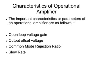
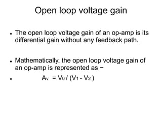
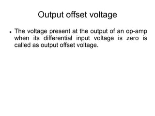
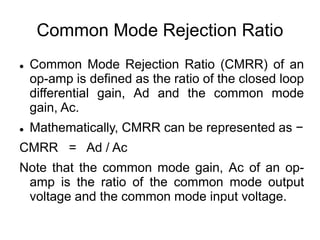
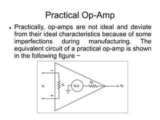
Analog Circuit
IC OP-AMP Applications
UNIT-II
ANUJ KUMAR SHARMA
Assistant Professor
Dept. of ECE ,FET GKV Haridwar
INDEX
 OP-AMP Fundamentals (brief review of differential
amplifier, current mirror, active load, level shifter, output
stage; ac and dc characteristics)
 Basic building blocks using OP-AMPS.
 Inverting/ Non-inverting VCVS,
 Integrators,
 Differentiators,
 CCVS and VCCS,
 Instrumentation Amplifiers.
Basics Of Operational Amplifier
 Operational Amplifier, also called as an Op-
Amp, is an integrated circuit, which can be used
to perform various linear, non-linear, and
mathematical operations. An op-amp is a direct
coupled high gain amplifier. You can operate
op-amp both with AC and DC signals.
Construction of Operational
Amplifier
 An op-amp consists of differential amplifier(s), a
level translator and an output stage. A
differential amplifier is present at the input stage
of an op-amp and hence an op-amp consists of
two input terminals. One of those terminals is
called as the inverting terminal and the other
one is called as the non-inverting terminal. The
terminals are named based on the phase
relationship between their respective inputs and
outputs.
Characteristics of Operational
Amplifier
 The important characteristics or parameters of
an operational amplifier are as follows −
 Open loop voltage gain
 Output offset voltage
 Common Mode Rejection Ratio
 Slew Rate
Open loop voltage gain
 The open loop voltage gain of an op-amp is its
differential gain without any feedback path.
 Mathematically, the open loop voltage gain of
an op-amp is represented as −
 Av = V0 / (V1 - V2 )
Output offset voltage
 The voltage present at the output of an op-amp
when its differential input voltage is zero is
called as output offset voltage.
Common Mode Rejection Ratio
 Common Mode Rejection Ratio (CMRR) of an
op-amp is defined as the ratio of the closed loop
differential gain, Ad and the common mode
gain, Ac.
 Mathematically, CMRR can be represented as −
CMRR = Ad / Ac
Note that the common mode gain, Ac of an op-
amp is the ratio of the common mode output
voltage and the common mode input voltage.
Slew Rate
 Slew rate of an op-amp is defined as the
maximum rate of change of the output voltage
due to a step input voltage.
 Mathematically, slew rate (SR) can be
represented as −
 SR = Maximum of dV0 / dt
 Where, V0 is the output voltage. In general,
slew rate is measured in either V/μSec or
V/mSec.
Types of Operational Amplifiers
 An op-amp is represented with a triangle
symbol having two inputs and one output.
 Op-amps are of two types: Ideal Op-Amp and
Practical Op-Amp.
 They are discussed in detail as given below −
Ideal Op-Amp
Conti...
 An ideal op-amp exhibits the following characteristics −
 Input impedance Zi =∞Ω
 Output impedance Z0 = 0Ω
 Open loop voltage gaine Av=∞
 If (the differential) input voltage Vi=0V, then the output
voltage will be V0=0V
 Bandwidth is infinity. It means, an ideal op-amp will amplify
the signals of any frequency without any attenuation.
 Common Mode Rejection Ratio (CMRR) is infinity.
 Slew Rate (SR) is infinity. It means, the ideal op-amp will
produce a change in the output instantly in response to an
input step voltage.
Practical Op-Amp
 Practically, op-amps are not ideal and deviate
from their ideal characteristics because of some
imperfections during manufacturing. The
equivalent circuit of a practical op-amp is shown
in the following figure −
Conti...
 A practical op-amp exhibits the following characteristics −
 Input impedance, Zi in the order of Mega ohms.
 Output impedance, Z0 in the order of few ohms..
 Open loop voltage gain, Av will be high.
Conti....
 When you choose a practical op-amp, you should check
whether it satisfies the following conditions −
 Input impedance, Zi should be as high as possible.
 Output impedance, Z0 should be as low as possible.
 Open loop voltage gain, Av should be as high as possible.
 Output offset voltage should be as low as possible.
 The operating Bandwidth should be as high as possible.
 CMRR should be as high as possible.
 Slew rate should be as high as possible.
Analog circuit Unit 2.ppt

Analog circuit Unit 2.ppt

  • 1.
    Analog Circuit IC OP-AMPApplications UNIT-II ANUJ KUMAR SHARMA Assistant Professor Dept. of ECE ,FET GKV Haridwar
  • 2.
    INDEX  OP-AMP Fundamentals(brief review of differential amplifier, current mirror, active load, level shifter, output stage; ac and dc characteristics)  Basic building blocks using OP-AMPS.  Inverting/ Non-inverting VCVS,  Integrators,  Differentiators,  CCVS and VCCS,  Instrumentation Amplifiers.
  • 3.
    Basics Of OperationalAmplifier  Operational Amplifier, also called as an Op- Amp, is an integrated circuit, which can be used to perform various linear, non-linear, and mathematical operations. An op-amp is a direct coupled high gain amplifier. You can operate op-amp both with AC and DC signals.
  • 4.
    Construction of Operational Amplifier An op-amp consists of differential amplifier(s), a level translator and an output stage. A differential amplifier is present at the input stage of an op-amp and hence an op-amp consists of two input terminals. One of those terminals is called as the inverting terminal and the other one is called as the non-inverting terminal. The terminals are named based on the phase relationship between their respective inputs and outputs.
  • 5.
    Characteristics of Operational Amplifier The important characteristics or parameters of an operational amplifier are as follows −  Open loop voltage gain  Output offset voltage  Common Mode Rejection Ratio  Slew Rate
  • 6.
    Open loop voltagegain  The open loop voltage gain of an op-amp is its differential gain without any feedback path.  Mathematically, the open loop voltage gain of an op-amp is represented as −  Av = V0 / (V1 - V2 )
  • 7.
    Output offset voltage The voltage present at the output of an op-amp when its differential input voltage is zero is called as output offset voltage.
  • 8.
    Common Mode RejectionRatio  Common Mode Rejection Ratio (CMRR) of an op-amp is defined as the ratio of the closed loop differential gain, Ad and the common mode gain, Ac.  Mathematically, CMRR can be represented as − CMRR = Ad / Ac Note that the common mode gain, Ac of an op- amp is the ratio of the common mode output voltage and the common mode input voltage.
  • 9.
    Slew Rate  Slewrate of an op-amp is defined as the maximum rate of change of the output voltage due to a step input voltage.  Mathematically, slew rate (SR) can be represented as −  SR = Maximum of dV0 / dt  Where, V0 is the output voltage. In general, slew rate is measured in either V/μSec or V/mSec.
  • 10.
    Types of OperationalAmplifiers  An op-amp is represented with a triangle symbol having two inputs and one output.  Op-amps are of two types: Ideal Op-Amp and Practical Op-Amp.  They are discussed in detail as given below −
  • 11.
  • 12.
    Conti...  An idealop-amp exhibits the following characteristics −  Input impedance Zi =∞Ω  Output impedance Z0 = 0Ω  Open loop voltage gaine Av=∞  If (the differential) input voltage Vi=0V, then the output voltage will be V0=0V  Bandwidth is infinity. It means, an ideal op-amp will amplify the signals of any frequency without any attenuation.  Common Mode Rejection Ratio (CMRR) is infinity.  Slew Rate (SR) is infinity. It means, the ideal op-amp will produce a change in the output instantly in response to an input step voltage.
  • 13.
    Practical Op-Amp  Practically,op-amps are not ideal and deviate from their ideal characteristics because of some imperfections during manufacturing. The equivalent circuit of a practical op-amp is shown in the following figure −
  • 14.
    Conti...  A practicalop-amp exhibits the following characteristics −  Input impedance, Zi in the order of Mega ohms.  Output impedance, Z0 in the order of few ohms..  Open loop voltage gain, Av will be high.
  • 15.
    Conti....  When youchoose a practical op-amp, you should check whether it satisfies the following conditions −  Input impedance, Zi should be as high as possible.  Output impedance, Z0 should be as low as possible.  Open loop voltage gain, Av should be as high as possible.  Output offset voltage should be as low as possible.  The operating Bandwidth should be as high as possible.  CMRR should be as high as possible.  Slew rate should be as high as possible.