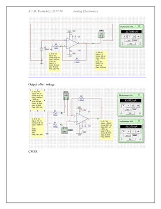
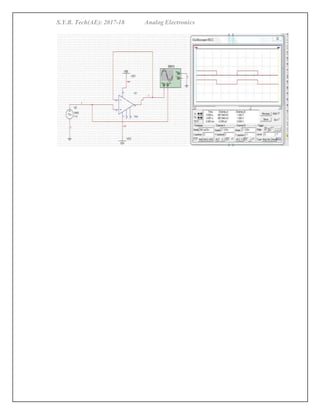
SlideShare a Scribd company logo
1 of 10
OP-AMP PARAMETERS
EXPERIMENT NO 5
Batch B1 Bock 1
Omkar Rane SETB118
Rohit Mane SETB102
Abhishek Sainkar SETB104
Tanmay Kale SETB112
AUGUST 8, 2017
MIT ACADEMY OF ENGINEERING, DEPARTMENT ENTC ENGG
ANALOG ELECTRONICS
S.Y.B. Tech(AE): 2017-18 Analog Electronics
EXPERIMENT No: 5
OP-AMP parameters
Fig. 1 Opamp Parameters
Offset Voltage:
A practical concern for op-amp performance is voltage offset. That is, effect of
having the output voltage something other than zero volts when the two input
terminals are shorted together. Remember that operational amplifiers are
differential amplifiers above all: they're supposed to amplify the difference in voltage
between the two input connections and nothing more.
Difference is exactly zero volts, we would (ideally) expect to have exactly zero volts
present on the output. However, in the real world this rarely happens. Even if the
op-amp in question has zero common-mode gain, the output voltage may not be at
zero when both inputs are shorted together.
This deviation from zero is called offset.A perfect op-amp would output exactly zero
volts with both its inputs shorted together and grounded. However, most op-amps
off the shelf will drive their outputs to a saturated level, either negative or positive.
Offset voltage will tend to introduce slight errorsin any op-amp circuit. So how do
we compensate for it? There are usually provisions made by the manufacturer to
trim the offset of a packaged op amp.
Usually, two extra terminals on the op-amp package are reserved for connecting an
external trim" potentiometer. These connection points are labeled offset null.
OP-Amp parameters FOR HIGH SPEED
operation & HIGH PERFORMANCE efficiency
Inputoffset
voltage
Inputbias
/offsetcurrent
Slew Rate CMRR
S.Y.B. Tech(AE): 2017-18 Analog Electronics
Fig. 2 Input offset voltage
Bias and Offset current:
Inputs on an op-amp have extremely high input impedances. That is, the input
currents entering or exiting an op-amp's two input signal connections are extremely
small. For most purposes of op-amp circuit analysis, we treat themas though they
don't exist at all.We analyze the circuit as though there wasabsolutely zero current
entering or exiting the input connections.
This idyllic picture, however, is not entirely true. Op-amps, especially those op-
amps with bipolar transistor inputs, have to have some amount of current through
their input connections in order for their internal circuits to be properly biased.
These currents, logically, are called bias currents.
The input bias current is the dc current required to properly operate the first stage
within the op-amp. The input impedance is another. Also, the input offset current
which can become a problem if both dc input currents are not the same.
Fig.3 Input bias current
The input offset current Ios, is the difference of the input bias currents,expressed
as an absolute value
Slew Rate
S.Y.B. Tech(AE): 2017-18 Analog Electronics
Slew rate is defined as the maximum rate of change of the output voltage under
large signal conditions. Expressed in units of volts per microsecond (V/us), the
slew rate is dependent on the frequency response of the internal stages of the
op-amp. Thus, the higher the slew rate, the better the frequency response of the
amplifier. The measurement of the operational amplifier’s slew rate is always
accomplished with a larger-signal amplifier having unity gain with a high-input
frequency signal. 𝑆𝑙𝑒𝑤 𝑅𝑎𝑡𝑒 =
∆𝑉𝑜𝑢𝑡
∆𝑡
(𝑣 𝜇𝑠⁄ )
Fig.4 Slew rate Measurement
CMRR
If the same signal is applied simultaneouslyto both inputs, called the common-
mode input, then the output voltage of an ideal op-amp should be zero. Since
operational amplifiers are not ideal devices, a small but finite output voltage will
be present whenboth the input voltages are the same. The ratio of the common-
mode input voltage to the generated output voltage is termed as common-mode
rejection ratio (CMRR) and is expressed in decibels. The higher the CMRR is the
better for the rejection and the smaller for the output voltage.
𝐶𝑀𝑅𝑅 = 20𝑙𝑜𝑔
𝐴𝑣(𝑑)
𝐴𝑣(𝑐𝑚)
(𝑑𝐵)
Fig.5CMRR Measurement
Pre Lab activity:
S.Y.B. Tech(AE): 2017-18 Analog Electronics
1. In Fig.2 Prove that








1
1
R
R
V
Vio
f
O
V1=V2=Vio
Vs=R1*Vio/(Rf + R1) – voltage divider rule
Avf= Vo/Vio=(Rf+R1)/R1= 1+Rf/R1
Vio=Vo/(1+Rf/R1)
2. Following is the circuit used for bias current measurement
Fig 6 Circuits to measure input bias currents Ib1 and Ib2, respectively.
a. Write the formula for Ib1 =V1/R1
b. Write the formula for Ib2=V2/R2
Lab Exercise: -
1. Circuit diagram of Offset voltage, bias and offset current, CMRR and Slew
rate measurement
2. Procedure: - (Write in your own words)
1) Use multisim software to draw various configuration of op amps.
2) The various op amp parameters are verified through various
configurations you have build that on multisim to calculate
theoretical and practical values.
3) Use various formula to figure out following parameters:
Ib1=V1/R1,
S.Y.B. Tech(AE): 2017-18 Analog Electronics
Ib2=V2/R2
A=Rf/Ri
Ib=(Ib1+Ib2)/2
Iios=|Ib1-Ib2|
Vid= Vi1-Vi2
Vod=Vid* A
CMRR= Ad/Ac
3. List the Equipment / Component required for the experiment
Equipment / Components Specifications/Values
Function Generator CADDO,4061,3MHz Pulse
Generator with 40 MHz Frequency
Counter
CRO HAL-TEC plus, HT4030,30MHz,
Oscilloscope
Resistor R= 1MΩ, 100kΩ, 10kΩ
Breadboard, wires
Variable Power Supply
Operational amplifier IC 741
Capacitor 0.1 farad, 0.01 farads ceramic
type
MULTISIM 12 0r 8
4. Observation Table (Multisim readings)
Parameters Practical
Datasheet
specifications
S.Y.B. Tech(AE): 2017-18 Analog Electronics
Input offset voltage 0.2 mV 1 mV
Voltage gain Av 10 2*105
Input bias current 14 mA 50 nA
Input resistance ∞ 2 MΩ
Output resistance 0 75 Ω
Input offset current 10 mA 20 nA
Slew rate ∞ 0.5 V/µsec
CMRR 58 dB 80 dB
Conclusion: -
We had studied various op amp parameters like slew rate, input bias current, input offset
current, input offset voltage, open loop gain. we had verified these parameters through
various op amps configuration.
Post Lab. Activity: -
1. List out parameters of Opamp OP07
S.Y.B. Tech(AE): 2017-18 Analog Electronics
2. What is the highest frequency of a triangle wave of 20-V peak-to-peak
amplitude that can be reproduced by an op amp whose slew rate is 10V/μs?
For a sine wave of the same frequency what is the maximum amplitude of
output signal that remain undistorted?
Answer:
Given : -
Slew Rate = 10V/μs2
VP-P = 20 volts
Solution: Type equation here.
Slew Rate = 2πf VP-P
10V/μs= 2πf 20
f =79 kHz
Now, Vp-p = Slew rate/2πf
= 10 / 2π(79kHz)
= 2.0146 x 10⁻⁵
Note :- Kindly attach screenshot of your performed experiments
Videos on OP -AMP Parameter:
https://youtu.be/TxBJb-Z0XFI
https://youtu.be/hq6e9v1ZYG4
S.Y.B. Tech(AE): 2017-18 Analog Electronics
Output offset voltage.
CMRR
S.Y.B. Tech(AE): 2017-18 Analog Electronics

More Related Content

What's hot (20)

Directional couplers 22
Directional couplers 22Directional couplers 22
Directional couplers 22
 
Electrodynamometer wattmeter
Electrodynamometer wattmeterElectrodynamometer wattmeter
Electrodynamometer wattmeter
 
Multivibrator
MultivibratorMultivibrator
Multivibrator
 
ANALOG TO DIGITAL AND DIGITAL TO ANALOG CONVERTER
ANALOG TO DIGITAL AND DIGITAL TO ANALOG CONVERTERANALOG TO DIGITAL AND DIGITAL TO ANALOG CONVERTER
ANALOG TO DIGITAL AND DIGITAL TO ANALOG CONVERTER
 
Differential amplifier
Differential amplifierDifferential amplifier
Differential amplifier
 
rectifiers
rectifiersrectifiers
rectifiers
 
Cascade and cascode amplifiers
Cascade and cascode amplifiersCascade and cascode amplifiers
Cascade and cascode amplifiers
 
6 slides
6 slides6 slides
6 slides
 
Operational amplifier
Operational amplifierOperational amplifier
Operational amplifier
 
Eye pattern
Eye patternEye pattern
Eye pattern
 
Analog to digital converters, adc
Analog to digital converters, adcAnalog to digital converters, adc
Analog to digital converters, adc
 
Design of IIR filters
Design of IIR filtersDesign of IIR filters
Design of IIR filters
 
LINEAR INTEGRATED CIRCUITS
LINEAR INTEGRATED CIRCUITSLINEAR INTEGRATED CIRCUITS
LINEAR INTEGRATED CIRCUITS
 
Tuned amplifire
Tuned amplifireTuned amplifire
Tuned amplifire
 
integrator and differentiator op-amp
integrator and differentiator op-ampintegrator and differentiator op-amp
integrator and differentiator op-amp
 
Op-Amp 1
Op-Amp 1Op-Amp 1
Op-Amp 1
 
quantization
quantizationquantization
quantization
 
Slew rate, Open and closed loop configurations
Slew rate, Open and closed loop configurationsSlew rate, Open and closed loop configurations
Slew rate, Open and closed loop configurations
 
Dsp lecture vol 7 adaptive filter
Dsp lecture vol 7 adaptive filterDsp lecture vol 7 adaptive filter
Dsp lecture vol 7 adaptive filter
 
Digital Filters Part 2
Digital Filters Part 2Digital Filters Part 2
Digital Filters Part 2
 

Similar to OP amp parameters

Unit-I Characteristics of opamp
Unit-I Characteristics of opampUnit-I Characteristics of opamp
Unit-I Characteristics of opampDr.Raja R
 
Electrical signal processing and transmission
Electrical signal processing and transmissionElectrical signal processing and transmission
Electrical signal processing and transmissionBishal Rimal
 
EC3451 LINEAR INTEGRATED CIRCUITS UNIT 1 .pdf
EC3451 LINEAR INTEGRATED CIRCUITS UNIT 1 .pdfEC3451 LINEAR INTEGRATED CIRCUITS UNIT 1 .pdf
EC3451 LINEAR INTEGRATED CIRCUITS UNIT 1 .pdfVanithaR25
 
ET191012(GENERAL VIVA presentatfvfvfvdfvfdvfio).pdf
ET191012(GENERAL VIVA presentatfvfvfvdfvfdvfio).pdfET191012(GENERAL VIVA presentatfvfvfvdfvfdvfio).pdf
ET191012(GENERAL VIVA presentatfvfvfvdfvfdvfio).pdfgffddffv vfdfvfvf
 
Exp no 3 setb118 Analog electronics
Exp no 3 setb118  Analog electronicsExp no 3 setb118  Analog electronics
Exp no 3 setb118 Analog electronicsOmkar Rane
 
Analog & Digital Integrated Circuits - Material (Short Answers)
Analog & Digital Integrated Circuits -  Material (Short Answers) Analog & Digital Integrated Circuits -  Material (Short Answers)
Analog & Digital Integrated Circuits - Material (Short Answers) Mathankumar S
 
Instrumentational Amplifier
Instrumentational Amplifier Instrumentational Amplifier
Instrumentational Amplifier ZunAib Ali
 
Kevin Glass Doctoral Qualifying Exam
Kevin Glass Doctoral Qualifying ExamKevin Glass Doctoral Qualifying Exam
Kevin Glass Doctoral Qualifying ExamKevin Glass
 
Kevin Glass Doctoral Qualifying Exam
Kevin Glass Doctoral Qualifying ExamKevin Glass Doctoral Qualifying Exam
Kevin Glass Doctoral Qualifying ExamKevin Glass
 
Ec6412 linear-integrated-circuit-laboratory
Ec6412 linear-integrated-circuit-laboratoryEc6412 linear-integrated-circuit-laboratory
Ec6412 linear-integrated-circuit-laboratoryPRADEEPJ30
 

Similar to OP amp parameters (20)

Unit-I Characteristics of opamp
Unit-I Characteristics of opampUnit-I Characteristics of opamp
Unit-I Characteristics of opamp
 
Sarah
SarahSarah
Sarah
 
Operational%20 amplifier
Operational%20 amplifierOperational%20 amplifier
Operational%20 amplifier
 
Electrical signal processing and transmission
Electrical signal processing and transmissionElectrical signal processing and transmission
Electrical signal processing and transmission
 
EC3451 LINEAR INTEGRATED CIRCUITS UNIT 1 .pdf
EC3451 LINEAR INTEGRATED CIRCUITS UNIT 1 .pdfEC3451 LINEAR INTEGRATED CIRCUITS UNIT 1 .pdf
EC3451 LINEAR INTEGRATED CIRCUITS UNIT 1 .pdf
 
Arvi
ArviArvi
Arvi
 
ET191012(GENERAL VIVA presentatfvfvfvdfvfdvfio).pdf
ET191012(GENERAL VIVA presentatfvfvfvdfvfdvfio).pdfET191012(GENERAL VIVA presentatfvfvfvdfvfdvfio).pdf
ET191012(GENERAL VIVA presentatfvfvfvdfvfdvfio).pdf
 
Analog Electronics.pptx
Analog Electronics.pptxAnalog Electronics.pptx
Analog Electronics.pptx
 
Exp no 3 setb118 Analog electronics
Exp no 3 setb118  Analog electronicsExp no 3 setb118  Analog electronics
Exp no 3 setb118 Analog electronics
 
Analog & Digital Integrated Circuits - Material (Short Answers)
Analog & Digital Integrated Circuits -  Material (Short Answers) Analog & Digital Integrated Circuits -  Material (Short Answers)
Analog & Digital Integrated Circuits - Material (Short Answers)
 
Op amp
Op ampOp amp
Op amp
 
Instrumentational Amplifier
Instrumentational Amplifier Instrumentational Amplifier
Instrumentational Amplifier
 
Arevalo
ArevaloArevalo
Arevalo
 
Report
ReportReport
Report
 
Qualprez
QualprezQualprez
Qualprez
 
Kevin Glass Doctoral Qualifying Exam
Kevin Glass Doctoral Qualifying ExamKevin Glass Doctoral Qualifying Exam
Kevin Glass Doctoral Qualifying Exam
 
Kevin Glass Doctoral Qualifying Exam
Kevin Glass Doctoral Qualifying ExamKevin Glass Doctoral Qualifying Exam
Kevin Glass Doctoral Qualifying Exam
 
Ec6412 linear-integrated-circuit-laboratory
Ec6412 linear-integrated-circuit-laboratoryEc6412 linear-integrated-circuit-laboratory
Ec6412 linear-integrated-circuit-laboratory
 
Op amp
Op ampOp amp
Op amp
 
Reyes
ReyesReyes
Reyes
 

More from Omkar Rane

Enabling SSL Elasticsearch on server
Enabling SSL Elasticsearch on serverEnabling SSL Elasticsearch on server
Enabling SSL Elasticsearch on serverOmkar Rane
 
Anti lock braking (ABS) Model based Design in MATLAB-Simulink
Anti lock braking (ABS) Model based Design in MATLAB-SimulinkAnti lock braking (ABS) Model based Design in MATLAB-Simulink
Anti lock braking (ABS) Model based Design in MATLAB-SimulinkOmkar Rane
 
Autosar fundamental
Autosar fundamentalAutosar fundamental
Autosar fundamentalOmkar Rane
 
Stress Management
Stress ManagementStress Management
Stress ManagementOmkar Rane
 
Bootloaders (U-Boot)
Bootloaders (U-Boot) Bootloaders (U-Boot)
Bootloaders (U-Boot) Omkar Rane
 
Concept of Diversity & Fading (wireless communication)
Concept of Diversity & Fading (wireless communication)Concept of Diversity & Fading (wireless communication)
Concept of Diversity & Fading (wireless communication)Omkar Rane
 
Tata Motors GDC .LTD Internship
Tata Motors GDC .LTD Internship Tata Motors GDC .LTD Internship
Tata Motors GDC .LTD Internship Omkar Rane
 
Machine Learning Model for M.S admissions
Machine Learning Model for M.S admissionsMachine Learning Model for M.S admissions
Machine Learning Model for M.S admissionsOmkar Rane
 
Timer 0 programming on LPC 1768
Timer 0 programming on LPC 1768Timer 0 programming on LPC 1768
Timer 0 programming on LPC 1768Omkar Rane
 
ADC (Analog to Digital conversion) using LPC 1768
ADC (Analog to Digital conversion) using LPC 1768ADC (Analog to Digital conversion) using LPC 1768
ADC (Analog to Digital conversion) using LPC 1768Omkar Rane
 
PWM based motor speed control using LPC 1768
PWM based motor speed control using LPC 1768PWM based motor speed control using LPC 1768
PWM based motor speed control using LPC 1768Omkar Rane
 
UART interfacing on LPC1768 (Cortex M3 micro controller)
UART interfacing on LPC1768 (Cortex M3 micro controller)UART interfacing on LPC1768 (Cortex M3 micro controller)
UART interfacing on LPC1768 (Cortex M3 micro controller)Omkar Rane
 
LED Blinking logic on LPC1768
LED Blinking logic on LPC1768LED Blinking logic on LPC1768
LED Blinking logic on LPC1768Omkar Rane
 
CAN interfacing on LPC1768 (ARM Cortex M3 based Micro controller)
CAN interfacing on LPC1768 (ARM Cortex M3 based Micro controller)CAN interfacing on LPC1768 (ARM Cortex M3 based Micro controller)
CAN interfacing on LPC1768 (ARM Cortex M3 based Micro controller)Omkar Rane
 
Vlisi Course project presentation:Keypad Scanner
Vlisi Course project presentation:Keypad ScannerVlisi Course project presentation:Keypad Scanner
Vlisi Course project presentation:Keypad ScannerOmkar Rane
 
VlSI course project report : Keypad Scanner
VlSI course project report : Keypad Scanner VlSI course project report : Keypad Scanner
VlSI course project report : Keypad Scanner Omkar Rane
 
LPC 1768 A study on Real Time clock features
LPC 1768 A study on Real Time clock featuresLPC 1768 A study on Real Time clock features
LPC 1768 A study on Real Time clock featuresOmkar Rane
 
Nexys4ddr rm FPGA board Datasheet
Nexys4ddr rm  FPGA board DatasheetNexys4ddr rm  FPGA board Datasheet
Nexys4ddr rm FPGA board DatasheetOmkar Rane
 
Linear Regression (Machine Learning)
Linear Regression (Machine Learning)Linear Regression (Machine Learning)
Linear Regression (Machine Learning)Omkar Rane
 
transmission gate based design for 2:1 Multiplexer in micro-wind
transmission gate based design for 2:1 Multiplexer in micro-windtransmission gate based design for 2:1 Multiplexer in micro-wind
transmission gate based design for 2:1 Multiplexer in micro-windOmkar Rane
 

More from Omkar Rane (20)

Enabling SSL Elasticsearch on server
Enabling SSL Elasticsearch on serverEnabling SSL Elasticsearch on server
Enabling SSL Elasticsearch on server
 
Anti lock braking (ABS) Model based Design in MATLAB-Simulink
Anti lock braking (ABS) Model based Design in MATLAB-SimulinkAnti lock braking (ABS) Model based Design in MATLAB-Simulink
Anti lock braking (ABS) Model based Design in MATLAB-Simulink
 
Autosar fundamental
Autosar fundamentalAutosar fundamental
Autosar fundamental
 
Stress Management
Stress ManagementStress Management
Stress Management
 
Bootloaders (U-Boot)
Bootloaders (U-Boot) Bootloaders (U-Boot)
Bootloaders (U-Boot)
 
Concept of Diversity & Fading (wireless communication)
Concept of Diversity & Fading (wireless communication)Concept of Diversity & Fading (wireless communication)
Concept of Diversity & Fading (wireless communication)
 
Tata Motors GDC .LTD Internship
Tata Motors GDC .LTD Internship Tata Motors GDC .LTD Internship
Tata Motors GDC .LTD Internship
 
Machine Learning Model for M.S admissions
Machine Learning Model for M.S admissionsMachine Learning Model for M.S admissions
Machine Learning Model for M.S admissions
 
Timer 0 programming on LPC 1768
Timer 0 programming on LPC 1768Timer 0 programming on LPC 1768
Timer 0 programming on LPC 1768
 
ADC (Analog to Digital conversion) using LPC 1768
ADC (Analog to Digital conversion) using LPC 1768ADC (Analog to Digital conversion) using LPC 1768
ADC (Analog to Digital conversion) using LPC 1768
 
PWM based motor speed control using LPC 1768
PWM based motor speed control using LPC 1768PWM based motor speed control using LPC 1768
PWM based motor speed control using LPC 1768
 
UART interfacing on LPC1768 (Cortex M3 micro controller)
UART interfacing on LPC1768 (Cortex M3 micro controller)UART interfacing on LPC1768 (Cortex M3 micro controller)
UART interfacing on LPC1768 (Cortex M3 micro controller)
 
LED Blinking logic on LPC1768
LED Blinking logic on LPC1768LED Blinking logic on LPC1768
LED Blinking logic on LPC1768
 
CAN interfacing on LPC1768 (ARM Cortex M3 based Micro controller)
CAN interfacing on LPC1768 (ARM Cortex M3 based Micro controller)CAN interfacing on LPC1768 (ARM Cortex M3 based Micro controller)
CAN interfacing on LPC1768 (ARM Cortex M3 based Micro controller)
 
Vlisi Course project presentation:Keypad Scanner
Vlisi Course project presentation:Keypad ScannerVlisi Course project presentation:Keypad Scanner
Vlisi Course project presentation:Keypad Scanner
 
VlSI course project report : Keypad Scanner
VlSI course project report : Keypad Scanner VlSI course project report : Keypad Scanner
VlSI course project report : Keypad Scanner
 
LPC 1768 A study on Real Time clock features
LPC 1768 A study on Real Time clock featuresLPC 1768 A study on Real Time clock features
LPC 1768 A study on Real Time clock features
 
Nexys4ddr rm FPGA board Datasheet
Nexys4ddr rm  FPGA board DatasheetNexys4ddr rm  FPGA board Datasheet
Nexys4ddr rm FPGA board Datasheet
 
Linear Regression (Machine Learning)
Linear Regression (Machine Learning)Linear Regression (Machine Learning)
Linear Regression (Machine Learning)
 
transmission gate based design for 2:1 Multiplexer in micro-wind
transmission gate based design for 2:1 Multiplexer in micro-windtransmission gate based design for 2:1 Multiplexer in micro-wind
transmission gate based design for 2:1 Multiplexer in micro-wind
 

Recently uploaded

SPICE PARK APR2024 ( 6,793 SPICE Models )
SPICE PARK APR2024 ( 6,793 SPICE Models )SPICE PARK APR2024 ( 6,793 SPICE Models )
SPICE PARK APR2024 ( 6,793 SPICE Models )Tsuyoshi Horigome
 
Gurgaon ✡️9711147426✨Call In girls Gurgaon Sector 51 escort service
Gurgaon ✡️9711147426✨Call In girls Gurgaon Sector 51 escort serviceGurgaon ✡️9711147426✨Call In girls Gurgaon Sector 51 escort service
Gurgaon ✡️9711147426✨Call In girls Gurgaon Sector 51 escort servicejennyeacort
 
Churning of Butter, Factors affecting .
Churning of Butter, Factors affecting  .Churning of Butter, Factors affecting  .
Churning of Butter, Factors affecting .Satyam Kumar
 
Architect Hassan Khalil Portfolio for 2024
Architect Hassan Khalil Portfolio for 2024Architect Hassan Khalil Portfolio for 2024
Architect Hassan Khalil Portfolio for 2024hassan khalil
 
main PPT.pptx of girls hostel security using rfid
main PPT.pptx of girls hostel security using rfidmain PPT.pptx of girls hostel security using rfid
main PPT.pptx of girls hostel security using rfidNikhilNagaraju
 
HARMONY IN THE HUMAN BEING - Unit-II UHV-2
HARMONY IN THE HUMAN BEING - Unit-II UHV-2HARMONY IN THE HUMAN BEING - Unit-II UHV-2
HARMONY IN THE HUMAN BEING - Unit-II UHV-2RajaP95
 
Introduction-To-Agricultural-Surveillance-Rover.pptx
Introduction-To-Agricultural-Surveillance-Rover.pptxIntroduction-To-Agricultural-Surveillance-Rover.pptx
Introduction-To-Agricultural-Surveillance-Rover.pptxk795866
 
GDSC ASEB Gen AI study jams presentation
GDSC ASEB Gen AI study jams presentationGDSC ASEB Gen AI study jams presentation
GDSC ASEB Gen AI study jams presentationGDSCAESB
 
Microscopic Analysis of Ceramic Materials.pptx
Microscopic Analysis of Ceramic Materials.pptxMicroscopic Analysis of Ceramic Materials.pptx
Microscopic Analysis of Ceramic Materials.pptxpurnimasatapathy1234
 
Call Girls Delhi {Jodhpur} 9711199012 high profile service
Call Girls Delhi {Jodhpur} 9711199012 high profile serviceCall Girls Delhi {Jodhpur} 9711199012 high profile service
Call Girls Delhi {Jodhpur} 9711199012 high profile servicerehmti665
 
HARMONY IN THE NATURE AND EXISTENCE - Unit-IV
HARMONY IN THE NATURE AND EXISTENCE - Unit-IVHARMONY IN THE NATURE AND EXISTENCE - Unit-IV
HARMONY IN THE NATURE AND EXISTENCE - Unit-IVRajaP95
 
Gfe Mayur Vihar Call Girls Service WhatsApp -> 9999965857 Available 24x7 ^ De...
Gfe Mayur Vihar Call Girls Service WhatsApp -> 9999965857 Available 24x7 ^ De...Gfe Mayur Vihar Call Girls Service WhatsApp -> 9999965857 Available 24x7 ^ De...
Gfe Mayur Vihar Call Girls Service WhatsApp -> 9999965857 Available 24x7 ^ De...srsj9000
 
VIP Call Girls Service Hitech City Hyderabad Call +91-8250192130
VIP Call Girls Service Hitech City Hyderabad Call +91-8250192130VIP Call Girls Service Hitech City Hyderabad Call +91-8250192130
VIP Call Girls Service Hitech City Hyderabad Call +91-8250192130Suhani Kapoor
 
INFLUENCE OF NANOSILICA ON THE PROPERTIES OF CONCRETE
INFLUENCE OF NANOSILICA ON THE PROPERTIES OF CONCRETEINFLUENCE OF NANOSILICA ON THE PROPERTIES OF CONCRETE
INFLUENCE OF NANOSILICA ON THE PROPERTIES OF CONCRETEroselinkalist12
 
Concrete Mix Design - IS 10262-2019 - .pptx
Concrete Mix Design - IS 10262-2019 - .pptxConcrete Mix Design - IS 10262-2019 - .pptx
Concrete Mix Design - IS 10262-2019 - .pptxKartikeyaDwivedi3
 
Artificial-Intelligence-in-Electronics (K).pptx
Artificial-Intelligence-in-Electronics (K).pptxArtificial-Intelligence-in-Electronics (K).pptx
Artificial-Intelligence-in-Electronics (K).pptxbritheesh05
 

Recently uploaded (20)

SPICE PARK APR2024 ( 6,793 SPICE Models )
SPICE PARK APR2024 ( 6,793 SPICE Models )SPICE PARK APR2024 ( 6,793 SPICE Models )
SPICE PARK APR2024 ( 6,793 SPICE Models )
 
9953056974 Call Girls In South Ex, Escorts (Delhi) NCR.pdf
9953056974 Call Girls In South Ex, Escorts (Delhi) NCR.pdf9953056974 Call Girls In South Ex, Escorts (Delhi) NCR.pdf
9953056974 Call Girls In South Ex, Escorts (Delhi) NCR.pdf
 
Gurgaon ✡️9711147426✨Call In girls Gurgaon Sector 51 escort service
Gurgaon ✡️9711147426✨Call In girls Gurgaon Sector 51 escort serviceGurgaon ✡️9711147426✨Call In girls Gurgaon Sector 51 escort service
Gurgaon ✡️9711147426✨Call In girls Gurgaon Sector 51 escort service
 
Churning of Butter, Factors affecting .
Churning of Butter, Factors affecting  .Churning of Butter, Factors affecting  .
Churning of Butter, Factors affecting .
 
Architect Hassan Khalil Portfolio for 2024
Architect Hassan Khalil Portfolio for 2024Architect Hassan Khalil Portfolio for 2024
Architect Hassan Khalil Portfolio for 2024
 
main PPT.pptx of girls hostel security using rfid
main PPT.pptx of girls hostel security using rfidmain PPT.pptx of girls hostel security using rfid
main PPT.pptx of girls hostel security using rfid
 
HARMONY IN THE HUMAN BEING - Unit-II UHV-2
HARMONY IN THE HUMAN BEING - Unit-II UHV-2HARMONY IN THE HUMAN BEING - Unit-II UHV-2
HARMONY IN THE HUMAN BEING - Unit-II UHV-2
 
Introduction-To-Agricultural-Surveillance-Rover.pptx
Introduction-To-Agricultural-Surveillance-Rover.pptxIntroduction-To-Agricultural-Surveillance-Rover.pptx
Introduction-To-Agricultural-Surveillance-Rover.pptx
 
GDSC ASEB Gen AI study jams presentation
GDSC ASEB Gen AI study jams presentationGDSC ASEB Gen AI study jams presentation
GDSC ASEB Gen AI study jams presentation
 
young call girls in Green Park🔝 9953056974 🔝 escort Service
young call girls in Green Park🔝 9953056974 🔝 escort Serviceyoung call girls in Green Park🔝 9953056974 🔝 escort Service
young call girls in Green Park🔝 9953056974 🔝 escort Service
 
Microscopic Analysis of Ceramic Materials.pptx
Microscopic Analysis of Ceramic Materials.pptxMicroscopic Analysis of Ceramic Materials.pptx
Microscopic Analysis of Ceramic Materials.pptx
 
Call Girls Delhi {Jodhpur} 9711199012 high profile service
Call Girls Delhi {Jodhpur} 9711199012 high profile serviceCall Girls Delhi {Jodhpur} 9711199012 high profile service
Call Girls Delhi {Jodhpur} 9711199012 high profile service
 
HARMONY IN THE NATURE AND EXISTENCE - Unit-IV
HARMONY IN THE NATURE AND EXISTENCE - Unit-IVHARMONY IN THE NATURE AND EXISTENCE - Unit-IV
HARMONY IN THE NATURE AND EXISTENCE - Unit-IV
 
Exploring_Network_Security_with_JA3_by_Rakesh Seal.pptx
Exploring_Network_Security_with_JA3_by_Rakesh Seal.pptxExploring_Network_Security_with_JA3_by_Rakesh Seal.pptx
Exploring_Network_Security_with_JA3_by_Rakesh Seal.pptx
 
Gfe Mayur Vihar Call Girls Service WhatsApp -> 9999965857 Available 24x7 ^ De...
Gfe Mayur Vihar Call Girls Service WhatsApp -> 9999965857 Available 24x7 ^ De...Gfe Mayur Vihar Call Girls Service WhatsApp -> 9999965857 Available 24x7 ^ De...
Gfe Mayur Vihar Call Girls Service WhatsApp -> 9999965857 Available 24x7 ^ De...
 
VIP Call Girls Service Hitech City Hyderabad Call +91-8250192130
VIP Call Girls Service Hitech City Hyderabad Call +91-8250192130VIP Call Girls Service Hitech City Hyderabad Call +91-8250192130
VIP Call Girls Service Hitech City Hyderabad Call +91-8250192130
 
INFLUENCE OF NANOSILICA ON THE PROPERTIES OF CONCRETE
INFLUENCE OF NANOSILICA ON THE PROPERTIES OF CONCRETEINFLUENCE OF NANOSILICA ON THE PROPERTIES OF CONCRETE
INFLUENCE OF NANOSILICA ON THE PROPERTIES OF CONCRETE
 
Concrete Mix Design - IS 10262-2019 - .pptx
Concrete Mix Design - IS 10262-2019 - .pptxConcrete Mix Design - IS 10262-2019 - .pptx
Concrete Mix Design - IS 10262-2019 - .pptx
 
Artificial-Intelligence-in-Electronics (K).pptx
Artificial-Intelligence-in-Electronics (K).pptxArtificial-Intelligence-in-Electronics (K).pptx
Artificial-Intelligence-in-Electronics (K).pptx
 
🔝9953056974🔝!!-YOUNG call girls in Rajendra Nagar Escort rvice Shot 2000 nigh...
🔝9953056974🔝!!-YOUNG call girls in Rajendra Nagar Escort rvice Shot 2000 nigh...🔝9953056974🔝!!-YOUNG call girls in Rajendra Nagar Escort rvice Shot 2000 nigh...
🔝9953056974🔝!!-YOUNG call girls in Rajendra Nagar Escort rvice Shot 2000 nigh...
 

OP amp parameters

  • 1. OP-AMP PARAMETERS EXPERIMENT NO 5 Batch B1 Bock 1 Omkar Rane SETB118 Rohit Mane SETB102 Abhishek Sainkar SETB104 Tanmay Kale SETB112 AUGUST 8, 2017 MIT ACADEMY OF ENGINEERING, DEPARTMENT ENTC ENGG ANALOG ELECTRONICS
  • 2. S.Y.B. Tech(AE): 2017-18 Analog Electronics EXPERIMENT No: 5 OP-AMP parameters Fig. 1 Opamp Parameters Offset Voltage: A practical concern for op-amp performance is voltage offset. That is, effect of having the output voltage something other than zero volts when the two input terminals are shorted together. Remember that operational amplifiers are differential amplifiers above all: they're supposed to amplify the difference in voltage between the two input connections and nothing more. Difference is exactly zero volts, we would (ideally) expect to have exactly zero volts present on the output. However, in the real world this rarely happens. Even if the op-amp in question has zero common-mode gain, the output voltage may not be at zero when both inputs are shorted together. This deviation from zero is called offset.A perfect op-amp would output exactly zero volts with both its inputs shorted together and grounded. However, most op-amps off the shelf will drive their outputs to a saturated level, either negative or positive. Offset voltage will tend to introduce slight errorsin any op-amp circuit. So how do we compensate for it? There are usually provisions made by the manufacturer to trim the offset of a packaged op amp. Usually, two extra terminals on the op-amp package are reserved for connecting an external trim" potentiometer. These connection points are labeled offset null. OP-Amp parameters FOR HIGH SPEED operation & HIGH PERFORMANCE efficiency Inputoffset voltage Inputbias /offsetcurrent Slew Rate CMRR
  • 3. S.Y.B. Tech(AE): 2017-18 Analog Electronics Fig. 2 Input offset voltage Bias and Offset current: Inputs on an op-amp have extremely high input impedances. That is, the input currents entering or exiting an op-amp's two input signal connections are extremely small. For most purposes of op-amp circuit analysis, we treat themas though they don't exist at all.We analyze the circuit as though there wasabsolutely zero current entering or exiting the input connections. This idyllic picture, however, is not entirely true. Op-amps, especially those op- amps with bipolar transistor inputs, have to have some amount of current through their input connections in order for their internal circuits to be properly biased. These currents, logically, are called bias currents. The input bias current is the dc current required to properly operate the first stage within the op-amp. The input impedance is another. Also, the input offset current which can become a problem if both dc input currents are not the same. Fig.3 Input bias current The input offset current Ios, is the difference of the input bias currents,expressed as an absolute value Slew Rate
  • 4. S.Y.B. Tech(AE): 2017-18 Analog Electronics Slew rate is defined as the maximum rate of change of the output voltage under large signal conditions. Expressed in units of volts per microsecond (V/us), the slew rate is dependent on the frequency response of the internal stages of the op-amp. Thus, the higher the slew rate, the better the frequency response of the amplifier. The measurement of the operational amplifier’s slew rate is always accomplished with a larger-signal amplifier having unity gain with a high-input frequency signal. 𝑆𝑙𝑒𝑤 𝑅𝑎𝑡𝑒 = ∆𝑉𝑜𝑢𝑡 ∆𝑡 (𝑣 𝜇𝑠⁄ ) Fig.4 Slew rate Measurement CMRR If the same signal is applied simultaneouslyto both inputs, called the common- mode input, then the output voltage of an ideal op-amp should be zero. Since operational amplifiers are not ideal devices, a small but finite output voltage will be present whenboth the input voltages are the same. The ratio of the common- mode input voltage to the generated output voltage is termed as common-mode rejection ratio (CMRR) and is expressed in decibels. The higher the CMRR is the better for the rejection and the smaller for the output voltage. 𝐶𝑀𝑅𝑅 = 20𝑙𝑜𝑔 𝐴𝑣(𝑑) 𝐴𝑣(𝑐𝑚) (𝑑𝐵) Fig.5CMRR Measurement Pre Lab activity:
  • 5. S.Y.B. Tech(AE): 2017-18 Analog Electronics 1. In Fig.2 Prove that         1 1 R R V Vio f O V1=V2=Vio Vs=R1*Vio/(Rf + R1) – voltage divider rule Avf= Vo/Vio=(Rf+R1)/R1= 1+Rf/R1 Vio=Vo/(1+Rf/R1) 2. Following is the circuit used for bias current measurement Fig 6 Circuits to measure input bias currents Ib1 and Ib2, respectively. a. Write the formula for Ib1 =V1/R1 b. Write the formula for Ib2=V2/R2 Lab Exercise: - 1. Circuit diagram of Offset voltage, bias and offset current, CMRR and Slew rate measurement 2. Procedure: - (Write in your own words) 1) Use multisim software to draw various configuration of op amps. 2) The various op amp parameters are verified through various configurations you have build that on multisim to calculate theoretical and practical values. 3) Use various formula to figure out following parameters: Ib1=V1/R1,
  • 6. S.Y.B. Tech(AE): 2017-18 Analog Electronics Ib2=V2/R2 A=Rf/Ri Ib=(Ib1+Ib2)/2 Iios=|Ib1-Ib2| Vid= Vi1-Vi2 Vod=Vid* A CMRR= Ad/Ac 3. List the Equipment / Component required for the experiment Equipment / Components Specifications/Values Function Generator CADDO,4061,3MHz Pulse Generator with 40 MHz Frequency Counter CRO HAL-TEC plus, HT4030,30MHz, Oscilloscope Resistor R= 1MΩ, 100kΩ, 10kΩ Breadboard, wires Variable Power Supply Operational amplifier IC 741 Capacitor 0.1 farad, 0.01 farads ceramic type MULTISIM 12 0r 8 4. Observation Table (Multisim readings) Parameters Practical Datasheet specifications
  • 7. S.Y.B. Tech(AE): 2017-18 Analog Electronics Input offset voltage 0.2 mV 1 mV Voltage gain Av 10 2*105 Input bias current 14 mA 50 nA Input resistance ∞ 2 MΩ Output resistance 0 75 Ω Input offset current 10 mA 20 nA Slew rate ∞ 0.5 V/µsec CMRR 58 dB 80 dB Conclusion: - We had studied various op amp parameters like slew rate, input bias current, input offset current, input offset voltage, open loop gain. we had verified these parameters through various op amps configuration. Post Lab. Activity: - 1. List out parameters of Opamp OP07
  • 8. S.Y.B. Tech(AE): 2017-18 Analog Electronics 2. What is the highest frequency of a triangle wave of 20-V peak-to-peak amplitude that can be reproduced by an op amp whose slew rate is 10V/μs? For a sine wave of the same frequency what is the maximum amplitude of output signal that remain undistorted? Answer: Given : - Slew Rate = 10V/μs2 VP-P = 20 volts Solution: Type equation here. Slew Rate = 2πf VP-P 10V/μs= 2πf 20 f =79 kHz Now, Vp-p = Slew rate/2πf = 10 / 2π(79kHz) = 2.0146 x 10⁻⁵ Note :- Kindly attach screenshot of your performed experiments Videos on OP -AMP Parameter: https://youtu.be/TxBJb-Z0XFI https://youtu.be/hq6e9v1ZYG4
  • 9. S.Y.B. Tech(AE): 2017-18 Analog Electronics Output offset voltage. CMRR
  • 10. S.Y.B. Tech(AE): 2017-18 Analog Electronics