
Recommended
More Related Content
Similar to Fundamentals of oprational Amplifiers.pptx
Similar to Fundamentals of oprational Amplifiers.pptx (20)
Recently uploaded
Recently uploaded (20)
Fundamentals of oprational Amplifiers.pptx
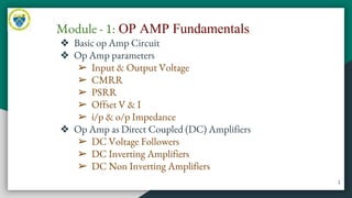
- 1. Module - 1: OP AMP Fundamentals ❖ Basic op Amp Circuit ❖ Op Amp parameters ➢ Input & Output Voltage ➢ CMRR ➢ PSRR ➢ Offset V & I ➢ i/p & o/p Impedance ❖ Op Amp as Direct Coupled (DC) Amplifiers ➢ DC Voltage Followers ➢ DC Inverting Amplifiers ➢ DC Non Inverting Amplifiers 1
- 2. ● Linear IC or Analog IC ● Versatile device, used for many Applications like ○ Signal Amplification ○ Oscillators ○ Multivibrators ○ Regulators ○ Peak Detectors ○ Mathematical operations like addition, Subtraction, Multiplication, Integration etc... 2 Introduction Op Amp Intro
- 3. 3 Symbol Five terminal ● Inverting Input terminal ● Non - Inverting Input terminal ● Output Voltage terminal ● + Supply Voltage terminal ● - Supply Voltage terminal Op Amp Intro
- 5. IC 741 Op Amp 5 Op Amp Intro
- 6. Blocks of Op Amp 6 Op Amp Intro
- 7. Practical Vs ideal Op - Amp Characteristics 7 Op Amp Intro
- 8. Modes of Operation 8 ❖ Inverting Mode ❖ Non - Inverting mode ❖ Differential mode Op Amp Intro
- 9. Inverting Mode 9 Vo = - AV * Vi Where Vo = o/p Voltage Vi = i/p Voltage & AV = open loop Voltage gain The negative sign indicates the phase shift of 180o between input and output signals Op Amp Intro
- 10. 10 Non - Inverting Mode Vo = AV * Vi Where Vo = o/p Voltage Vi = i/p Voltage & AV = open loop Voltage gain Op Amp Intro
- 11. 11 Differential Mode Vd = (V1 - V2) Vo = AV * Vd Vo = AV * (V1 - V2) Where Vo = o/p Voltage V1 = i/p Voltage applied to + terminal V2 = i/p Voltage applied to - terminal & AV = open loop Voltage gain Op Amp Intro
- 12. To produce a 5 V output voltage, find the required voltage difference between the input terminals of 741 op amp. Assume Av = 2,00,000 12 5V AV ? Sol: Vo = AV * Vd Op Amp Intro
- 13. Basic Operational Amplifier Circuit 13 Differential amplifier stage Emitter Follower o/p Basic Op Amp Circuit
- 14. 14 Assume Q1 and Q2 are Identical transistors i.e. VBE1 = VBE2 & 𝛽1 = 𝛽2 Q1 and Q2 bases at GND lvl Then IE1 = IE2 Both emitter currents flows through RE.. With Q1 and Q2 bases Grounded So, Vo = VCC - VRC - VBE3 Basic Op Amp Circuit
- 15. Ex. 1: Given VCC = +10V, VEE = -10V, RE = 4.7 kΩ, RC = 6.8 kΩ, and all transistors have VBE = 0.7V, Find the output voltage Vo assuming both Q1 and Q2 bases are at GND lvl. 15 IE1 = IE2 = 1mA Then, IC1 = IC2 ≈ 1mA Vo = VCC - VRC - VBE3 = 10 - 1m*6.8k - 0.7 = 2.5 V Basic Op Amp Circuit
- 16. 16 Basic Op Amp Circuit Consider a + tive going voltage is applied to #3. Q1 base is Pulled up by the i/p Voltage. Q1 Emitter tends to follow the i/p Voltage. ∵ Q1 and Q2 emitters are tied together, Q2 emitter is also pulled up. VBE2 is reduced So, IC2 will decrease. Vo = VCC - VRC - VBE3 From this Expression, VRC will reduce due to reduction of IC2, ⇒ Vo ↑ So, a +tive going voltage to non - inverting terminal(#3) will increase the output voltage and vice versa.
- 17. 17 Basic Op Amp Circuit Ex. 2: Assume that the Positive going input voltage at the base of Q1 in Ex. 1 reduces the IC2 by 0.2mA, (i.e., from 1mA to 0.8mA). Determine the new output voltage. Vo = VCC - VRC - VBE3 = 10 - 0.8m*6.8k - 0.7 = 3.9V. The output voltage Vo changes from 2.5 V to 3.9V. Vo ↑
- 18. 18 Basic Op Amp Circuit Consider a + tive going voltage is applied to #2. Q2 base is Pulled up by the i/p Voltage. Q2 Emitter tends to follow the i/p Voltage. ∵ Q1 and Q2 emitters are tied together, Q1 emitter is also pulled up. VBE2 is Increased. So, IC2 will increase. Vo = VCC - VRC - VBE3 From this Expression, VRC will increase due to increase of IC2, ⇒ Vo ↓ So, a +tive going voltage to inverting terminal(#2) will decrease the output voltage and vice versa.
- 19. 19 Basic Op Amp Circuit Ex. 3: Assume that the Positive going input voltage at the base of Q2 in Ex. 1 Increases the IC2 by 0.2mA, (i.e., from 1mA to 1.2mA). Determine the new output voltage. Vo = VCC - VRC - VBE3 = 10 - 1.2m*6.8k - 0.7 = 1.1V The output voltage Vo changes from 2.5 V to 1.1V. Vo ↓
- 20. 20 Op Amp Circuit The Voltage Follower Circuit The Voltage Follower circuit Basic Op AMP as Voltage follower
- 21. 21 Op Amp Circuit The o/p terminal(#6) is connected to the inverting i/p terminal(#2). With #3 at GND lvl, #2 and the output (#6) must also be at GND lvl If consider the o/p lvl is to move slightly above GND lvl, ➔ the base of Q2 would be higher than the base of Q1. ➔ IC2↑, leads to VRC ↑ ➔ Pushing the Vo down until VB1 = VB2 And Vice versa., This above theory holds good, if the input voltage is applied to #3 Thus the output follows the input.
- 22. 22 Op Amp Circuit Due to high internal voltage gain, a small difference between the i/p and the o/p. To produce the o/p closely to the i/p, the differential i/p voltage is Where, M is the open loop voltage gain The Exact o/p voltage be then Vo = Vi - Vd
- 23. 23
- 24. 24 Op Amp Circuit Ex. 4: A 741 IC op amp is connected to function as a voltage follower. The input signal is 1V. Assuming the amplifier gain is the only error source, determine the o/p voltage that occurs with an op amp which has a). Typical gain, b) Minimum gain. Vo = Vi - Vd = 1 - 5μ = 0.999 995 V For a typical gain of 2,00,000 For a Minimum gain of 50,000 Vo = Vi - Vd = 1 - 20μ = 0.999 98 V
- 25. 25 Op Amp Circuit The Non Inverting Amplifier Non Inverting Amplifier Basic Op AMP as Non Inverting Amplifier
- 26. 26 Op Amp Circuit Works similar way as that of Voltage follower. Difference is, instead of all the output fed back to the inverting terminal, a portion of output is fed back. The Vo is potentially divided across resistors, R2 & R3. When Vi = GND: ➔ #2, also in GND lvl ➔ If not, any voltage difference will be amplified to move the inverting as well as the #6 at GND lvl.
- 27. 27 Op Amp Circuit ➔ VR3 = 0V ➔ The current I2 through R2 & R3 =0mA ➔ ∴ Vo = 0V When Vi = 100mV ➔ The output voltage Vo moves to a level that makes the feedback voltage to #2 equal to 100mV. VR3 = Vi = I2 R3 Vo = I2(R2 + R3)
- 28. 28 Op Amp Circuit Ex. 5: An op-amp non inverting amplifier as illustrated in fig., has R2 as 8.2kΩ and R3, as 150Ω. Calculate the amplifier voltage gain, and determine a new resistance value for R3 to give a gain of 75. = 55.7 ≃111Ω
- 29. 29 Op Amp Circuit The Inverting Amplifier Inverting Amplifier Basic Op AMP as Inverting Amplifier
- 30. 30 Op Amp Circuit ➔ Because #3 is at GND lvl, #2 also at GND lvl ➔ #2 is Virtual grounded ➔ So the input signal Vi is dropping across R1 & the output signal Vo is dropping across R2. Vi = I1 R1 Vo = - I1 R2
- 31. 31 Op Amp Circuit Ex. 6: An op-amp inverting amplifier as illustrated in fig., has R1 as 270Ω and R2, as 8.2 kΩ. Calculate the amplifier voltage gain, and determine a new resistance value for R1 to give a gain of 60.
- 32. 32 Op Amp Parameters Input Voltage Range
- 33. 33 Op Amp Parameters The Maximum +tive going and -tive going input voltage that may be applied to an operational amplifier is termed as Input Voltage Range .
- 34. 34 Op Amp Parameters Output Voltage Range
- 35. 35 Op Amp Parameters The Rough approximation for most of the Operational Amplifiers is that the Maximum output swing is approximately equal to 1V less than the supply voltage
- 36. 36 Op Amp Parameters Power Supply Voltage Rejection The power supply rejection ratio (PSRR) is a measure of how effective the operational amplifier is in dealing with the variations in supply voltage (changes in +VCC & -VEE). If a variation of 1V in VCC or VEE causes the output to change by 1V, then PSSR = 1V per volt (1 V/V). For 741 op amp, the PSRR is typically 30 μV/V, &, for LM 108 the supply voltage rejection is 96dB.
- 37. 37 Op Amp Circuit Ex. 7: A 741 operational amplifier uses a ± 15V supply with a 2mV, 120 Hz ripple voltage superimposed. Calculate the amplitude of the output voltage produced by the power supply ripple. Vo(rip) = VS(rip) * PSRR = 2 mV * 30 μV/V = 60 nV
- 38. 38 Op Amp Parameters Input Offset Voltage For the output voltage to be exactly as that of input, Q1 and Q2 must be a perfect match. Vo = Vi - VBE1 + VBE2 With VBE1 = VBE2, & Vi = 0V Vo = 0V Consider VBE1 = 0.7 V & VBE2 = 0.6V Now Vo = -0.1V This unwanted output is known as an Output offset Voltage. To set Vo to Gnd lvl, the input would have to be raised to 0.1V. This is termed as Input offset Voltage(Vos) In voltage follower circuit, the output and the Inverting terminal follow the voltage at the non inverting input.
- 39. 39 Op Amp Parameters Input Offset Current If Q1 and Q2 i/p transistors are not a perfect match, then their current gain (hfe) will not be the same. Thus, when both transistors have equal collector current, the base current will never be same. For ex., the base current of one might be 1 μA and the other might be 1.2 μA. The difference in these two current levels is known as the Input offset current (Ios)
- 40. 40 Op Amp Parameters Input Impedance For all linear applications, some forms of negative feedback is provided externally connected components. The input impedance with negative feedback is given as Zin = (1 + Mβ) Zi Where , Zi = the op amp i/p impedance without -tive feedback M = op amp open loop gain β = feedback factor
- 41. 41 Op Amp Parameters Output Impedance For all linear applications, some forms of negative feedback is provided externally connected components. The output impedance with negative feedback is given as Where , Zo = the op amp o/p impedance without -tive feedback M = op amp open loop gain β = feedback factor.
- 43. 43 Op Amp Circuit Ex. 8: For a 741 operational amplifier Voltage follower, calculate the Minimum input impedance. Also calculate the typical output impedance of the same. For voltage follower, Feedback factor β = 1. Zin = (1 + Mβ) Zi Zi(Min) = 0.3 MΩ & MMin = 50,000 Zin = (1 + 50000 * 1 ) 0.3 *106 = 15 000 MΩ Zo(Typ) = 75Ω & MTyp = 2 00 000. = 37✕ 10-5 Ω
- 44. 44 Op Amp Parameters Slew Rate Slew rate (S) of an operational amplifier is the Maximum rate at which the output voltage can change. When the slew rate is too slow for the input, distortion results. Sine wave input to a voltage follower producing a triangular output due to less slew rate.
- 45. 45 Op Amp Parameters Slew Rate cont... The Typical slew rate(S) for a 741 opamp is 0.5 V per microsec. i.e., for the output to change by 0.5V, 1μs is required for 741 op amp. The equation relating time, voltage change and the slew rate is Ex. 9: For a 741 operational amplifier Voltage follower, calculate the Minimum time required to change the output voltage by 10V = 20μs
- 46. 46 Op Amp Parameters CMRR Considering the base of Q1 and Q2 are raised to 1V above ground The voltage drop across the emitter resistor RE is increased by 1 V, and So, IC1 and IC2 are increased. changing the output voltage. (Vo ≠ 0 V) The two input terminals are connected together and both are raised by 1V above the Ground level. This is known as a Common Mode Input. Now the differential input(Vd) is Zero; So ideally the operational amplifier should be Zero.
- 47. 47 Op Amp Parameters CMRR cont.. The common mode gain (ACM) is the ratio of output voltage changes due to the common mode input to the common mode input The success of an op-amp in rejecting the common mode inputs is defined in the common mode rejection ratio (CMRR). CMRR is the ratio of the open-loop gain (M) to the common mode gain (ACM). The CMRR is usually expressed as a decibel quantity on the op-amp data sheet. typical CMRR for the 741 op-amp is 96 dB
- 48. 48 DC coupled Amplifiers Direct Coupled Voltage Followers a resistor R1 is frequently used in series with the inverting terminal to match the source resistance RS in series with the non inverting terminal.
- 49. 49 DC coupled Amplifiers Need of Voltage follower a high impedance source to a low impedance load. Part of VS is lost when a low impedance load is directly connected to the high impedance source
- 50. 50 DC coupled Amplifiers Direct Coupled Voltage Followers Zin = (1 + Mβ) Zi ∵ Zin ≫ RS; Vi ≅ VS ∵ Zout ≪ RL; Vo ≅ Vi Vo = Vi - Vd As Vd is very very less; Vo≅ Vi
- 51. 51
- 52. 52 DC coupled Amplifiers Ex. 10: A voltage follower using a 741 op-amp, is connected to a signal source of 1 V via a 47 kΩ resistor and a 20 kΩ load. calculate the load voltage when a) The load is directly connected to the source b) The voltage follower is between the load and the source.
- 53. 53 DC coupled Amplifiers DC Source without Voltage Follower Fig a: RL directly connected to VCC The load voltage VL derived directly from the VCC VL varies if there is any variation in the RL
- 54. 54 DC coupled Amplifiers Constant DC Source with a voltage follower Fig b: Constant voltage source using voltage follower A potential divider with a voltage follower produces a constant load voltage irrespective of any variations in RL. The voltage input to the voltage follower is the drop across R2. So, Vo = VL will be effectively V2 itself, irrespective of RL variations.
- 55. 55 DC coupled Amplifiers Ex. 11: 1 kΩ load is to have 5 V developed across it from a 15 V source. Design suitable circuits as shown in fig (a) and (b) and calculate the load voltage variations in each case when the load resistance varies by -10%. Use 741 op amp for circuit (b).
- 56. 56 DC coupled Amplifiers Direct - Coupled Non inverting Amplifiers DC Noninverting Amplifier The input signal VS is connected directly to the non inverting terminal (#3) of the op- amp via a resistor R1. The R1 is included to equalize the IBR drops at the op-amp inputs.
- 57. 57 DC coupled Amplifiers Design For a 741 op-amp: Choose I2 >> IB(max) = 100 ×IB(max) ∵ VR3 = Vi, In case of BiFET op-amps having the bias current very very less, the largest resistor is first selected as 1 MΩ and then finds the current I2. The output Vo appears across (R2 + R3), R1 = R2 ∥ R3
- 58. 58 DC coupled Amplifiers Ex. 12: Using a 741 op-amp, design a noninverting amplifier to have a voltage gain of approximately 66. The input signal amplitude is to be 15 mV. For a 741 op-amp: Choose I2 >> IB(max) = 100 ×IB(max) = 100 × 500 nA = 50μA ∵ VR3 = Vi, VR3 Vo = VR2 = Vo - VR3 = R2 =
- 59. 59 DC coupled Amplifiers Ex. 13: Redesign the noninverting amplifier in the previous example using a LF353 BiFET op-amp. For a BiFET op-amp, the largest resistor is chosen as 1 MΩ. For a voltage gain of 66, R2 is the largest resistor, So R2 = 1 MΩ.
- 60. 60 DC coupled Amplifiers Direct - Coupled Non inverting Amplifiers DC Noninverting Amplifier with i/p & o/p impedance The input impedance of the op-amp circuit with a negative feedback is given as Zin = (1 + M × β) Zi For a noninverting amplifier, the feedback factor, β is given as
- 61. 61 DC coupled Amplifiers Direct - Coupled inverting Amplifiers DC inverting Amplifier The inverting amplifier includes R3 at the non inverting terminal to equalize the IBR drops at the op-amp inputs. R3 = R1 ∥ R2 If R1 is not much larger as compared to RS, then R3 =(R1 + RS) ∥ R2 The gain of this circuit is given as
- 62. Direct Coupled Inverting Amplifiers 62 Design Steps:for 741 op-amp Current I1 is to be selected much higher than IB(max) Choose I1>> IB(max) = 100 ×IB(max) R1 = Vi/I1 ; R2 = Vo/I1 R3 = R1 ∥ R2 If R1 is not much larger as compared to RS, then R3 =(R1 + RS) ∥ R2
- 63. Direct Coupled Inverting Amplifiers 63 Design of Direct Coupled Inverting Amplifier for LF353 BiFET op-amp: For BiFET op-amps select the largest resistor value as 1 MΩ R1=R2/Av R3=R1 ॥ R2 Av = - R2/R1
- 64. Direct Coupled Inverting Amplifiers 64 INPUT AND OUTPUT IMPEDANCE OF DIRECT COUPLED INVERTING AMPLIFIER The Resistor R1 is seen with its other end at Ground level. Zin = R1.
- 65. Direct Coupled Inverting Amplifiers 65 Ex. 14: Design an inverting amplifier using a 741 op-amp.The voltage gain is to be 50 and the output voltage amplitude is to be 2.5 V.
- 66. Direct Coupled Inverting Amplifiers 66 Ex. 15: Redesign the inverting amplifier in the previous example using a LF353 BiFET op-amp.