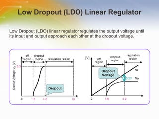
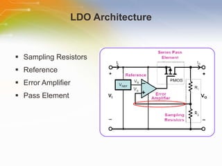
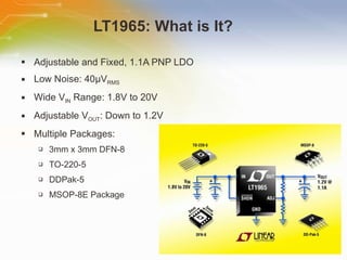
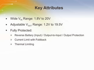
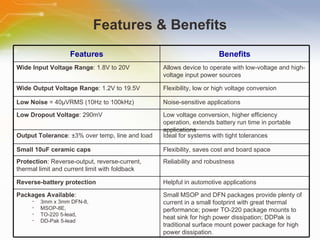
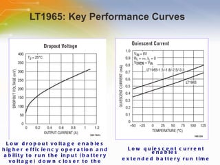
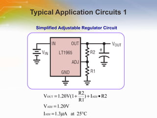
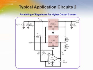
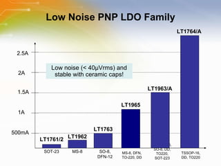
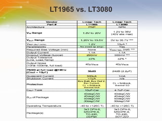
LT1965    – Low Noise LDO Linear Regulator Source: LINEAR TECHNOLOGY
Introduction Purpose To introduce the LT1965 low noise, low dropout linear regulator Outline Introduction to Low Dropout voltage regulator Overview of the LT1965 Application circuits Comparison with the LT1965 & LT3080 Content 14 pages
Low Dropout (LDO) Linear Regulator Low Dropout (LDO) linear regulator regulates the output voltage until its input and output approach each other at the dropout voltage.
LDO Architecture Sampling Resistors Reference Error Amplifier Pass Element
LT1965: What is It?  Adjustable and Fixed, 1.1A PNP LDO Low Noise: 40µV RMS   Wide V IN  Range: 1.8V to 20V Adjustable V OUT : Down to 1.2V  Multiple Packages: 3mm x 3mm DFN-8 TO-220-5 DDPak-5 MSOP-8E Package
Key Attributes Wide V IN  Range: 1.8V to 20V  Adjustable V OUT  Range: 1.2V to 19.5V Fully Protected: Reverse Battery (Input) / Output-to-Input / Output Protection Current Limit with Foldback Thermal Limiting
Features & Benefits Features Benefits Wide Input Voltage Range :  1.8V to 20V Allows device to operate with low-voltage and high-voltage input power sources Wide Output Voltage Range : 1.2V to 19.5V Flexibility, low or high voltage conversion Low Noise  = 40µVRMS (10Hz to 100kHz) Noise-sensitive applications Low Dropout Voltage : 290mV  Low voltage conversion, higher efficiency operation, extends battery run time in portable applications  Output Tolerance : ±3% over temp, line and load  Ideal for systems with tight tolerances  Small 10uF ceramic caps   Flexibility, saves cost and board space  Protection : Reverse-output, reverse-current, thermal limit and current limit with foldback  Reliability and robustness  Reverse-battery protection  Helpful in automotive applications  Packages Available : 3mm x 3mm DFN-8, MSOP-8E, TO-220 5-lead, DD-Pak 5-lead  Small MSOP and DFN packages provide plenty of current in a small footprint with great thermal performance; power TO-220 package mounts to heat sink for high power dissipation; DDPak is traditional surface mount power package for high power dissipation.
LT1965: Key Performance Curves Low dropout voltage enables higher efficiency operation and ability to run the input (battery voltage) down closer to the output voltage while maintaining regulation Low quiescent current enables  extended battery run time
Output Voltage Noise In most systems, the range of 10Hz to 100kHz is the information signal processing area of concern. Linear regulators produce little noise energy outside this region. Output voltage noise of the LT1965 is approximately 80nV/√Hz over this frequency bandwidth. For higher output voltages, the output voltage noise gains up accordingly.
Typical Application Circuits 1 Simplified Adjustable Regulator Circuit
Typical Application Circuits 2 Paralleling of Regulators for Higher Output Current
Low Noise PNP LDO Family MS-8 SO-8, DFN-12 TSSOP-16, SO-8, DD, TO220, SOT-223 TSSOP-16, DD, TO220 MS-8, DFN, TO-220, DD 500mA 1A 1.5A 2.5A LT1761/2 LT1763 LT1963/A 2A SOT-23 LT1962 LT1764/A Low   noise   (<   40 μ Vrms)   and   stable   with   ceramic   caps! LT1965
LT1965 vs. LT3080
Additional Resource For ordering the LT1965, please click the part list or Call our sales hotline For additional inquires contact our technical service hotline For more product information go to http://www.linear.com/pc/productDetail.jsp?navId=H0,C1,C1003,C1040,C1055,P38628 Newark Farnell

LT1965 - Low Noise LDO Linear Regulator

  • 1.
    LT1965 – Low Noise LDO Linear Regulator Source: LINEAR TECHNOLOGY
  • 2.
    Introduction Purpose Tointroduce the LT1965 low noise, low dropout linear regulator Outline Introduction to Low Dropout voltage regulator Overview of the LT1965 Application circuits Comparison with the LT1965 & LT3080 Content 14 pages
  • 3.
    Low Dropout (LDO)Linear Regulator Low Dropout (LDO) linear regulator regulates the output voltage until its input and output approach each other at the dropout voltage.
  • 4.
    LDO Architecture SamplingResistors Reference Error Amplifier Pass Element
  • 5.
    LT1965: What isIt? Adjustable and Fixed, 1.1A PNP LDO Low Noise: 40µV RMS Wide V IN Range: 1.8V to 20V Adjustable V OUT : Down to 1.2V Multiple Packages: 3mm x 3mm DFN-8 TO-220-5 DDPak-5 MSOP-8E Package
  • 6.
    Key Attributes WideV IN Range: 1.8V to 20V Adjustable V OUT Range: 1.2V to 19.5V Fully Protected: Reverse Battery (Input) / Output-to-Input / Output Protection Current Limit with Foldback Thermal Limiting
  • 7.
    Features & BenefitsFeatures Benefits Wide Input Voltage Range : 1.8V to 20V Allows device to operate with low-voltage and high-voltage input power sources Wide Output Voltage Range : 1.2V to 19.5V Flexibility, low or high voltage conversion Low Noise = 40µVRMS (10Hz to 100kHz) Noise-sensitive applications Low Dropout Voltage : 290mV Low voltage conversion, higher efficiency operation, extends battery run time in portable applications Output Tolerance : ±3% over temp, line and load Ideal for systems with tight tolerances Small 10uF ceramic caps Flexibility, saves cost and board space Protection : Reverse-output, reverse-current, thermal limit and current limit with foldback Reliability and robustness Reverse-battery protection Helpful in automotive applications Packages Available : 3mm x 3mm DFN-8, MSOP-8E, TO-220 5-lead, DD-Pak 5-lead Small MSOP and DFN packages provide plenty of current in a small footprint with great thermal performance; power TO-220 package mounts to heat sink for high power dissipation; DDPak is traditional surface mount power package for high power dissipation.
  • 8.
    LT1965: Key PerformanceCurves Low dropout voltage enables higher efficiency operation and ability to run the input (battery voltage) down closer to the output voltage while maintaining regulation Low quiescent current enables extended battery run time
  • 9.
    Output Voltage NoiseIn most systems, the range of 10Hz to 100kHz is the information signal processing area of concern. Linear regulators produce little noise energy outside this region. Output voltage noise of the LT1965 is approximately 80nV/√Hz over this frequency bandwidth. For higher output voltages, the output voltage noise gains up accordingly.
  • 10.
    Typical Application Circuits1 Simplified Adjustable Regulator Circuit
  • 11.
    Typical Application Circuits2 Paralleling of Regulators for Higher Output Current
  • 12.
    Low Noise PNPLDO Family MS-8 SO-8, DFN-12 TSSOP-16, SO-8, DD, TO220, SOT-223 TSSOP-16, DD, TO220 MS-8, DFN, TO-220, DD 500mA 1A 1.5A 2.5A LT1761/2 LT1763 LT1963/A 2A SOT-23 LT1962 LT1764/A Low noise (< 40 μ Vrms) and stable with ceramic caps! LT1965
  • 13.
  • 14.
    Additional Resource Forordering the LT1965, please click the part list or Call our sales hotline For additional inquires contact our technical service hotline For more product information go to http://www.linear.com/pc/productDetail.jsp?navId=H0,C1,C1003,C1040,C1055,P38628 Newark Farnell

Editor's Notes

  • #3 Welcome to the training module on Linear Technology’s LT1965 Low Noise LDO Linear Regulator. This training module introduces the LT1965 low noise, low dropout linear regulator, and its key features and benefits.
  • #4 In an increasing trend, telecommunications, networking, audio and instrumentation require low noise power supplies. In particular, there is interest in low dropout linear regulators or LDO. Dropout voltage is defined as the minimum input-to-output voltage difference where output voltage of the LDO regulators remains regulated. That is, the LDO regulates the output voltage until its input and output approach each other at the dropout voltage. Ideally, the dropout voltage should be as low as possible to minimize power dissipation and maximize efficiency. As shown in the figure, the working region for LDO is the “regulation region”, where it can provide a steady output voltage in a wide range of load current.
  • #5 LDO architecture can be as basic and simple as this figure. The main components are a power semiconductor and a differential amplifier (error amplifier). One input of the error amplifier monitors a percentage of the output as determined the resistor ratio of R1 and R2. The second input to the differential amplifier is from a stable voltage reference (V REF ). Therefore, the output voltage Vo will be set to a stable level according to R1, R2 and V REF . When there is a change at Vo, it will cause the divided feedback voltage (in red circle), through R1 and R2, to force the error amplifier to adjust the current flow through the series pass element. The Vo will be gradually regulated to the default stable level.
  • #6 The LT1965 is a 1.1A, adjustable and fixed output voltage PNP based LDO regulator. It offers high power density, low noise, wide input &amp; output voltage, good PSRR, low dropout, and has the bullet-proof arsenal of protection features. The LT1965 has low dropout voltage of only 300mV at full load, with wide VIN capability of 1.8V to 20V and low adjustable output from 1.2V to 19.5V. The ultra-low output noise of only 40uV-RMS reduces noise in instrumentation, RF, DSP &amp; logic supply systems and is also beneficial for post-regulating switching power supplies.
  • #7 The LT1965’s most important market differentiators are its wide input voltage range from 1.8V to 20V and an adjustable output from 1.2V to 19.5V. It also has a set of internal protection circuitry including reverse-battery protection, reverse current protection, current limiting with foldback, and thermal limiting.
  • #8 The LT1965 is a low noise, low input &amp; output voltage, 1.1 amp LDO. It features a low dropout voltage of only 290mV at full load, with wide input voltage range of 1.8V to 20V. The output is adjustable from 1.2V to 19.5V. An ultra-low output noise of only 40uV-RMS, reduces noise in instrumentation, RF, DSP and logic supply systems and is also beneficial for post-regulating switching power supplies. Output tolerance is tightly regulated to within ±3% over line, load and temperature. The device’s low quiescent current of 500uA at operation and less than 1uA at shutdown, makes it an excellent choice for applications requiring high output drive capability with low current consumption. The LT1965 regulator, optimizes stability and transient response, with a low ESR ceramic output capacitors as small as 10uF. These tiny external capacitors, can be used without any necessary series resistance as is common with many other regulators. Internal protection circuitry includes reverse-battery, reverse current, reverse output, current limiting with foldback, and thermal limiting. For applications requiring large input-to-output differentials, the LT1965 offers a very compact and thermally effective solution. The IC, features a wide breadth of packaging options, ranging from modern high power density, small footprint, thermally efficient DFN and MSOP packages, to more traditional D2-Pak and TO-220 power packaging. Operating junction temperature range is -40°C to +125°C.
  • #9 As shown in the left chart, the device is capable of supplying up to 1.1 amps at a typical dropout voltage of 310mV. The LT1965’s low dropout voltage allows for higher efficiency operation as the differential between input and output may be minimized and thus reducing power dissipation. Battery life, in portable products may be increased as the input voltage may be run down closer to the output voltage, and still maintain Vout regulation. The right chart illustrates the relationship between quiescent current and temperature. At +25 ºC, the operating quiescent current is around 500 μA for the adjustable version and 600μA for the fixed version. The low operating quiescent current drops to less than 1μA in shutdown.
  • #10 The LT1965 regulators have very low output noise, which makes them ideal for sensitive RF and DSP supply applications. In most systems, the range of 10Hz to 100kHz is the information signal processing area of concern. Normally, linear regulators produce very little noise-energy outside this region. The LT1965 regulators, are designed to provide low-output-voltage-noise over this bandwidth, while operating at full load. Output voltage noise is approximately 80nV per Hz over the frequency bandwidth for the adjustable LT1965. For higher output voltages the output voltage noise goes up accordingly.
  • #11 Here is a sample application circuit. As you can see, the LT1965, is easily configured as a general-purpose, high input voltage to low output adjustable regulator. It requires only 4 small external components. The ratio of two external resistors, R1 and R2, sets the output voltage. The device servos the output to maintain the ADJ pin voltage at 1.20V referenced to ground. The bias current of 1.3μA at 25 º C, flows through R2 and into the ADJ pin. Use the equation as shown in the page to calculate the output voltage.
  • #12 Here is another example to show how two or more devices can be hooked up in parallel to provide higher output current with the aid of an operational amplifier and some external passive components.
  • #13 The LT1965 may be thought of, as a lower current version of the LT1963/A, and a higher current version of the LT1763, which are all part of Linear Technology’s PNP LDO regulator family.
  • #14 The closest LDO in the LT portfolio, current-wise, is the LT3080 which is also rated up to 1.1 amps. The table lists the differences between the LT1965 and the LT3080. The first difference is the architecture. The LT1965 uses a PNP transistor while the LT3080 uses a NPN transistor. Other differences include dropout voltage, protection features and output accuracy. In addition, the LT1965 requires an external op amp, while the LT3080 is directly paralleled. LT1965 has a voltage-reference while the LT3080 has a current reference. These LDOs are targeted at different end applications. The LT3080 is more designed for surface mount systems, direct paralleling and ease-of-use, whereas the LT1965 is more for general-purpose conversion under potentially harsher conditions.
  • #15 Thank you for taking the time to view this presentation on “ LT1965 Low Noise LDO Linear Regulator” . If you would like to learn more or go on to purchase some of these devices, you may either click on the part list link, or simply call our sales hotline. For more technical information you may either visit the Linear Technology site, or if you would prefer to speak to someone live, please call our hotline number, or even use our ‘live chat’ online facility.